Gildas Martial Ngaleu | Charles Hubert Kom* | Aurélien Tamtsia Yeremou | Samuel Eke | Arnaud Nanfak
© 2021 IIETA. This article is published by IIETA and is licensed under the CC BY 4.0 license (http://creativecommons.org/licenses/by/4.0/).
OPEN ACCESS
In this paper, two new duty-cycle modulator structures are proposed, as a good alternative to existing modulation techniques: the symmetrical linear duty-cycle modulator, and the general linear duty-cycle modulator. The proposed structures consist of two stages with operational amplifiers and theirs period and duty cycle depend on the control voltage. The first stage is a Schmitt trigger comparator which generates the modulated rectangular signal. The other, by integrating the difference between modulated and reference signals, generates a triangular signal is which is sent back to the input of the comparator. To evaluate the performance of the proposed structures, a detailed study of sinusoidal pulse width modulator, non-inverting duty-cycle modulator and they were made. The simulation results computed in MATLAB/Simulink software show that proposed modulator scan operate in low frequency range, maintaining a constant current ripple and an acceptable total harmonic distortion. Their duty-cycles are independent of the values of the passive components used. The experimental tests carried out on symmetrical linear duty-cycle modulator under various reference voltage confirms the robustness of the structure in relation to the values of the components.
duty-cycle modulation, pulse width modulation, industrials applications
Modulation is an operation that consists of transposing asignal representing one information into another, without significantly modifying the information it carries. It transforms a modulating or primary signal into a modulated signal. A convention links the characteristics of the modulating signal to those of the modulated signal. Modulation theory has a major research area in signal transmission, signal processing, Analog-to-Digital Conversion (ADC), Digital-to-Analog Conversion (DAC) and control of power electronic converters and continues to attract considerable attention and interest [1]. The switching modulation which includes Sigma-Delta Modulation (SDM) Pulse Width Modulation (PWM) and Duty-Cycle Modulation (DCM) is a type of modulation widely used for industrial applications.
The pioneering complete SDM architecture was invented in 1962 by Janssen and Roermund [2]. The operation of SDM relies on the combination of two signal processing techniques, namely, oversampling and quantization error filtering and feedback, commonly referred as noise shaping [3]. Initially limited to the encoding of low-frequency audio signals and first- or second-order loop filtering, improved architectures and relevant applications of SDM technology have been increasingly developed by many authors, e.g., Goodman in 1969 [4], Jayant in 1976 [5], Hauser in 1991 [6], and Shreier et al. in 2017 [7]. However, the most modern application of SDM technology remain limited to ADC systems [8].
PWM is a modulation technique in which the frequency can be either constant or variable [9]. In constant frequency PWM method, the frequency is constant and the ON time changes according to the modulating signal. It can be produced by comparing a reference signal with a carrier signal [9]. In variable frequency PWM method, the frequency is variable and ON time or OFF time is constant. There are several different PWM techniques, differing in their methods of implementation. The basics PWM topologies including single PWM produced by comparing rectangular reference wave with triangular carrier wave, the multiple PWM and the Sinusoidal PWM (SPWM)using sinusoidal reference wave and triangular carrier wave [10]. There are several advanced PWM topologies depending on the carrier used such as Alternative Phase Opposite Disposition PWM (APOD-PWM), Harmonic-Injection PWM (HI-PWM), Carrier Based Space Vector PWM (CB-SVPWM) and stepped modulation [10, 11]. Although PWM is still widely used in industrial applications [12, 13], it still has some limitations. When PWM is used to control solid state switches, a relatively high frequency carrier is required to reduce current and voltage ripple and THD [14]. This increase in frequency leads to switching losses [15-17] on the one hand, and to thermal stress at the switches on the other hand [14, 18]. Today there are solutions to overcome this undesirable effect, such as the use of newer "big gap" switches, which have lower switching losses than silicon Insulated Gate Bipolar Transistor (IGBT) switches, but at a high cost [14]. Another solution would be to reduce the switching frequency without increasing ripple.
The DCM is a modulation in which an input signal x is transformed into a train of switching wave where duty cycle and period of the modulated signal vary simultaneously according to control signal [8, 19]. Initially invented and patented by Biard in 1962, the realization of classical DCM circuit requires at least two integrated circuits and seven passive elements [20]. A new simplest and higher quality DMC have subsequently been proposed by Mbihi et al. [21]. Initially proposed for instrumentation problems, they are today used in many sectors such as ADC [22, 23], DAC [24], control of electronic power converter [25, 26], digital signal transmission [19], power quality [27] and optical transmission [28]. This structure, although functional and allowing low-frequency operation, has some drawbacks, among which: The non-linearity of the function linking the duty-cycle to the control signal and the dependence of the duty-cycle on the values of the passive components.
In this article, we propose two new duty-cycle modulator structures namely Symmetrical Linear DCM (SLDCM) and General Linear DCM (GLDCM). These structures combining the advantages of PWM and DCM structures, are based on an association between an integrator circuit and a hysteresis comparator.
The remaining part of this paper is organized as follows: A brief description of SPWM and Non-Inverter DCM (NIDCM) is given in section 2. Section 3 is devoted to description and analysis of proposed DCM schemes. Section 4 present the simulation results and experimental validation and finally, section 5 concludes the paper.
Among the PWM techniques, the SPWM technique is one the most widely used. Nevertheless, in the last decade, the NIDCM gives many good results in several applications. This section describes in detail the SPWM and of NIDCM techniques in terms of relationship between period, duty cycle, reference voltage and all components of the structure.
2.1 Sinusoidal pulse width modulation technique
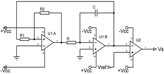
The scheme of a PWM signal generator is shown in Figure 1. It consists toa triangular signal generator which produces a carrier and an inverting comparator whose output switches as a function of the difference between the carrier and the control signal Vref, where R1, R2 and R are resistors and Ca capacitor. The saturation voltages of the amplifiers are +Vsat and -Vsat while +VCC and -VCC are their supply voltages; Vs is the output of the modulator.
Figure 1. Conventional pulse-width modulator
The period T and duty cycle a (with inverting comparator) of a PWM modulated signal are given by:
$T=4RC\frac{{{R}_{1}}}{{{R}_{2}}}$ (1)
$\alpha =\frac{1}{2}\left( 1+\frac{{{V}_{ref}}}{{{V}_{sat}}}\frac{{{R}_{2}}}{{{R}_{1}}} \right)$ (2)
For Vref =0V, we have$\alpha =\frac{1}{2}$.
The duty-cycle being between 0 and 1, we have:
$\left| \begin{matrix} \alpha =0\Rightarrow {{V}_{ref}}=-\frac{{{R}_{1}}}{{{R}_{2}}}{{V}_{sat}} \\ \alpha =1\Rightarrow {{V}_{ref}}=+\frac{{{R}_{1}}}{{{R}_{2}}}{{V}_{sat}} \\\end{matrix} \right.$ (3)
so,
$-\frac{{{R}_{1}}}{{{R}_{2}}}{{V}_{sat}}\le {{V}_{ref}}\le +\frac{{{R}_{1}}}{{{R}_{2}}}{{V}_{sat}}$ (4)
The ratio of the resistors R1 and R2 reduces the resolution of the reference voltage and consequently the resolution of the duty cycle.
2.2 Non-inverter duty-cycle modulation technique
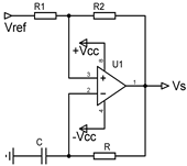
The scheme of the duty-cycle modulator developed by Mbihi et al is shown in Figure 2.
Figure 2. Non-inverter duty-cycle modulator
This modulator has the advantage of being simpler than a PWM modulator. Its period T and duty cycle a are defined by [21]:
$T=RC\ln \left( \frac{{{\left( {{\alpha }_{2}}{{V}_{ref}} \right)}^{2}}-{{\left( \left( {{\alpha }_{1}}+1 \right){{V}_{sat}} \right)}^{2}}}{{{\left( {{\alpha }_{2}}{{V}_{ref}} \right)}^{2}}-{{\left( \left( {{\alpha }_{1}}-1 \right){{V}_{sat}} \right)}^{2}}} \right)$ (5)
$\alpha =\frac{\ln \left( \frac{{{\alpha }_{2}}{{V}_{ref}}-\left( {{\alpha }_{1}}+1 \right){{V}_{sat}}}{{{\alpha }_{2}}{{V}_{ref}}-\left( {{\alpha }_{1}}-1 \right){{V}_{sat}}} \right)}{\ln \left( \frac{{{\left( {{\alpha }_{2}}{{V}_{ref}} \right)}^{2}}-{{\left( \left( {{\alpha }_{1}}+1 \right){{V}_{sat}} \right)}^{2}}}{{{\left( {{\alpha }_{2}}{{V}_{ref}} \right)}^{2}}-{{\left( \left( {{\alpha }_{1}}-1 \right){{V}_{sat}} \right)}^{2}}} \right)}$ (6)
With,
$\left| \begin{matrix} {{\alpha }_{1}}=\frac{{{R}_{1}}}{{{R}_{1}}+{{R}_{2}}} \\ {{\alpha }_{2}}=\frac{{{R}_{2}}}{{{R}_{1}}+{{R}_{2}}} \\\end{matrix} \right.$ (7)
There is considerable non-linearity in the expressions of the period and the duty cycle. By linearizing the duty cycle ratio around $0$(Vref =0 and $\alpha =\frac{1}{2}$) we have:
$\alpha =\frac{1}{2}\left( 1+\frac{{{V}_{ref}}}{{{V}_{sat}}}\frac{\frac{2{{\alpha }_{1}}}{\left( 1+{{\alpha }_{1}} \right)}}{\ln \left( \frac{1+{{\alpha }_{1}}}{1-{{\alpha }_{1}}} \right)} \right)$ (8)
The linearized expression of the duty cycle is only valid for a range of the control voltage Vref [ 23], which will reduce the resolution of the reference voltage and consequently the resolution of the duty cycle.
The minimum and central period and duty cycle (for Vref =0V) of the Linearized NIDCM (LNIDCM)are given by:
$\left| \begin{matrix} {{T}_{0}}=2RC\ln \left( 1+2\frac{{{R}_{1}}}{{{R}_{2}}} \right) \\ \alpha =\frac{1}{2} \\\end{matrix} \right.$ (9)
This section presents the different development leading to the relationships between period, duty cycle, components values and reference voltage for SLDCM and GLDCM.
3.1 Symmetrical Linear Duty-Cycle Modulation (SLDCM)
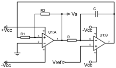
The SLCDM scheme is shown in Figure 3. It is the result of a modification of the signal generator used in SPWM structure. The hysteresis comparator always generates the modulated signal and the integrator generates, by integrating the difference between modulated and reference signals, a triangular signal that is feedback to the input of the comparator.
Figure 3. Symmetrical Linear Duty-Cycle Modulation (SLDCM)
This structure is simpler than the conventional pulse width modulator and has only one more component than the non-inverting duty-cycle modulator.
The trigger switching voltages are the solutions of the equation below:
${{v}_{0}}{{R}_{2}}+{{V}_{S}}{{R}_{1}}=0$ (10)
${{v}_{0}}=-\frac{{{R}_{1}}}{{{R}_{2}}}{{V}_{S}}$ (11)
With v0 the voltage at the output of the integrator and at the input of the Schmitt trigger.
As${{V}_{S}}=\pm {{V}_{sat}}$, and by calling $v_{0}^{+}$ and $v_{0}^{-}$ the switching voltages (respectively positive and negative), we get:
$\left| \begin{matrix} v_{0}^{+}=+\frac{{{R}_{1}}}{{{R}_{2}}}{{V}_{sat}} \\ v_{0}^{-}=-\frac{{{R}_{1}}}{{{R}_{2}}}{{V}_{sat}} \\\end{matrix} \right.$ (12)
The current in the capacitor C is defined by:
${{i}_{C}}=\frac{{{V}_{S}}-{{V}_{ref}}}{R}=C\frac{d{{v}_{C}}}{dt}$ (13)
where, vc is the voltage across the capacitor.
The output voltage v0 of the integrator is given by:
${{v}_{0}}={{V}_{ref}}-{{v}_{C}}\Leftrightarrow {{v}_{C}}={{V}_{ref}}-{{v}_{0}}$ (14)
so,
$\frac{{{V}_{S}}-{{V}_{ref}}}{R}=\frac{C}{dt}\left( d{{V}_{ref}}-d{{v}_{0}} \right)$ (15)
$dt=\frac{RC}{{{V}_{S}}-{{V}_{ref}}}\left( d{{V}_{ref}}-d{{v}_{0}} \right)$ (16)
For a constant value of Vref,
$d{{V}_{ref}}=0\Rightarrow dt=-\frac{RC}{{{V}_{S}}-{{V}_{ref}}}d{{v}_{0}}$ (17)
Let call tON and tOFF be the positive and negative pulse width respectively.
During tON, ${{V}_{S}}=+{{V}_{sat}}$ and v0 goes from v0+ to v0-; then,
${{t}_{ON}}=-\frac{RC}{{{V}_{sat}}-{{V}_{ref}}}\int_{v_{0}^{+}}^{v_{0}^{-}}{d{{v}_{0}}}$ (18)
${{t}_{ON}}=2RC\frac{{{R}_{1}}}{{{R}_{2}}}\frac{{{V}_{sat}}}{{{V}_{sat}}-{{V}_{ref}}}$ (19)
During tOFF, ${{V}_{S}}=-{{V}_{sat}}$ and v0 goes from v0- to v0+; then,
${{t}_{OFF}}=-\frac{RC}{-{{V}_{sat}}-{{V}_{ref}}}\int_{v_{0}^{-}}^{v_{0}^{+}}{d{{v}_{0}}}$ (20)
${{t}_{OFF}}=2RC\frac{{{R}_{1}}}{{{R}_{2}}}\frac{{{V}_{sat}}}{{{V}_{sat}}+{{V}_{ref}}}$ (21)
The period T of output voltage VS is given by:
$T={{t}_{ON}}+{{t}_{OFF}}$ (22)
$T=4RC\frac{{{R}_{1}}}{{{R}_{2}}}\frac{V_{sat}^{2}}{V_{sat}^{2}-V_{ref}^{2}}$ (23)
Its duty cycle is equal to:
$\alpha =\frac{{{t}_{ON}}}{T}$ (24)
$\alpha =\frac{1}{2}\left( 1+\frac{{{V}_{ref}}}{{{V}_{sat}}} \right)$ (25)
In view to Eq. (25), the duty-cycle ratio of the SLDCM is linear and independent of the values of the passive components. In this configuration, the control voltage can cover the entire range of supply voltages (for -Vsat to +Vsat), so the resolution is maximum.
Its minimum or central period and duty cycle (when Vref=0V) are given by:
$\left| \begin{matrix} {{T}_{0}}=4RC\frac{{{R}_{1}}}{{{R}_{2}}} \\ \alpha =\frac{1}{2} \\\end{matrix} \right.$ (26)
3.2 General Linear Duty-Cycle Modulation (GLDCM)
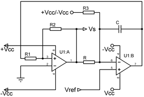
By adding a single resistor to the circuit in Figure 3 as shown in Figure 4 below, we can choose to scan the duty cycle for a voltage range defined in [-Vsat; +Vsat].
Figure 4. General Linear Duty-Cycle Modulation (GLDCM)
Depending on if we wish to use control voltages in the range $\left[ {{V}_{ref\min }};+{{V}_{sat}} \right]$ or in the range $\left[ -{{V}_{sat}};{{V}_{ref\max }} \right]$, R3 will be connected to +Vsat or -Vsat respectively. We have for a constant value of Vref:
${{i}_{C}}=\frac{{{V}_{S}}-{{V}_{ref}}}{R}+\frac{k{{V}_{sat}}-{{V}_{ref}}}{{{R}_{3}}}=-C\frac{d{{v}_{0}}}{dt}$ (27)
With k=1 when R3 is connected to +Vsat and k=-1 when R3 is connected to -Vsat. Then,
$dt=-\frac{R{{R}_{3}}C}{R\left( k{{V}_{sat}}-{{V}_{ref}} \right)+{{R}_{3}}\left( {{V}_{S}}-{{V}_{ref}} \right)}d{{v}_{0}}$ (28)
From the above we have,
${{t}_{ON}}=2RC\frac{{{R}_{1}}}{{{R}_{2}}}\frac{{{R}_{3}}{{V}_{sat}}}{\left( {{R}_{3}}+kR \right){{V}_{sat}}-\left( {{R}_{3}}+R \right){{V}_{ref}}}$ (29)
${{t}_{OFF}}=2RC\frac{{{R}_{1}}}{{{R}_{2}}}\frac{{{R}_{3}}{{V}_{sat}}}{\left( {{R}_{3}}-kR \right){{V}_{sat}}+\left( {{R}_{3}}+R \right){{V}_{ref}}}$ (30)
So, the period and duty cycle of general linear duty cycle modulator are:
$T=4RC\frac{{{R}_{1}}}{{{R}_{2}}}\frac{R_{3}^{2}V_{sat}^{2}}{\left( \begin{align} & \left( R_{3}^{2}-{{R}^{2}} \right)V_{sat}^{2}-{{\left( {{R}_{3}}+R \right)}^{2}}V_{ref}^{2} \\ & +2k\left( {{R}_{3}}R+{{R}^{2}} \right){{V}_{sat}}{{V}_{ref}} \\\end{align} \right)}$ (31)
And,
$\alpha =\frac{\left( {{R}_{3}}-kR \right){{V}_{sat}}+\left( {{R}_{3}}+R \right){{V}_{ref}}}{2{{R}_{3}}{{V}_{sat}}}$ (32)
This configuration of the linear DCM is more complete than the previous one. Indeed, if we make R3 tend towards infinity, we find the scheme and equations of the SLDCM modulator.
For$\alpha =\frac{1}{2}$, the minimum or central period T0 and the corresponding control voltage ${{V}_{ref0}}$ of GLDCM are given by:
$\left| \begin{matrix} {{T}_{0}}=4RC\frac{{{R}_{1}}}{{{R}_{2}}} \\ {{V}_{ref0}}=\frac{kR}{R+{{R}_{3}}}{{V}_{sat}} \\\end{matrix} \right.$ (33)
The values${{V}_{ref\min }}$ when (k=1) and${{V}_{ref\max }}$ when (k=-1) of Vref are obtained for a=0 and a=1 respectively. We have:
$\left| \begin{matrix} {{V}_{ref\min }}=\frac{R-{{R}_{3}}}{R+{{R}_{3}}}{{V}_{sat}} \\ {{V}_{ref\max }}=\frac{{{R}_{3}}-R}{{{R}_{3}}+R}{{V}_{sat}} \\\end{matrix} \right.$ (34)
In the particular case where R3=R,
$\left| \begin{matrix} {{V}_{ref\min }}={{V}_{ref\max }}=0 \\ {{V}_{ref0}}=\frac{k}{2}{{V}_{sat}} \\ T=RC\frac{{{R}_{1}}}{{{R}_{2}}}\frac{V_{sat}^{2}}{k{{V}_{sat}}{{V}_{ref}}-V_{ref}^{2}} \\ {{T}_{0}}=4RC\frac{{{R}_{1}}}{{{R}_{2}}} \\ \alpha =\frac{\left( 1-k \right){{V}_{sat}}+2{{V}_{ref}}}{2{{V}_{sat}}} \\\end{matrix} \right.$ (35)
In this case, we have for k=1:
$\alpha =\frac{{{V}_{ref}}}{{{V}_{sat}}}$ (36)
And for k=-1:
$\alpha =1+\frac{{{V}_{ref}}}{{{V}_{sat}}}$ (37)
This section will present the simulations and experimental results based on the equations developed in section 3. Itbegins with a comparison between SPWM, NIDCM and SLDCM. These comparisons were carried out with simulation models in MATLAB/Simulink environment. Next, the experimental tests result of proposed SLDCM structure will be discussed.
4.1 Modulators parameters
Simulations and experimental test were carried out under the specifications found in Table 1 below.
Table 1. Values of the passive components used
|
Modulators |
Passive components |
|||
|
R1 |
R2 |
R |
C |
|
|
SPWM NIDCM SLDCM |
10kΩ 10kΩ 10kΩ |
20kΩ 20kΩ 20kΩ |
5.000kΩ 7.213kΩ 5.000kΩ |
100nF 100nF 100nF |
These values were chosen to have a frequency of 1000 Hz for the SPWM and a maximum (center) frequency of 1000 Hz for the NIDCM and SLDCM.
4.2 Simulation results
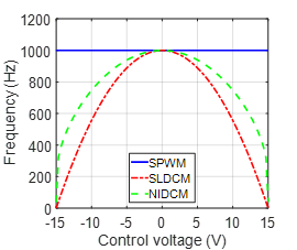
In Figure 5, the oscillation frequency computed according to Eqns. (1), (5) and (23) is constant for the PWM while it is variable depending to the control voltage for the duty cycle modulators. This variation is fully parabolic for the symmetrical linear DCM and partially parabolic for the non-inverting DCM. Looking at Figure 6 based on Eqns. (2), (6), (8) and (25), it can be seen that the duty cycles of the SPWM and SLDCM vary linearly as a function of the control signal. That of the NIDCM presents a range of linearity in a control range of approximately -9V to +9V, in which its curve is confused with that of its linearized expression LNIDCM; beyond this range, a non-linearity of the duty cycle is observed.
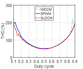
Although the expression of the SPWM duty cycle is linear, it does not cover the whole range of the control signal and is limited between -7.5V and +7.5V unlike the SLDCM which sweeps the whole control range from -15Vto +15V. As shown in Figure 7, the SLDCM as well as the SPWM and the NIDCM all have close THDs for the same values of the duty cycle. Figure 8 presents the output voltages for different control signal values.
Figure 5. Frequency versus control voltage
Figure 6. Duty cycle versus control voltage
Figure 7. THD versus duty cycle
Figure 8. Output voltage of modulators versus duty cycle
The values 0.35, 0.5 and 0.75 of the duty cycles correspond respectively to voltages of -5V, 0V and 7.5V for the SLDCM. It can be seen from the analysis of graphs that for duty cycles other than 0.5, the period and the associated control voltage are different for each modulator. For a=0.50, we have a frequency of 1000 Hz and a control voltage of 0V.
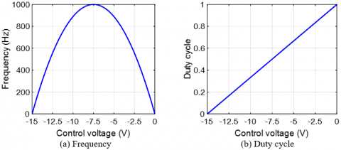
Figures 9 and 10 based on Eqns. (31) and (32) present the evolution of the frequency and the duty-cycle ratio of the GLDCM versus the control voltage for k=1 and k=-1 respectively, with R3=R.
Figure 9. Frequency and duty cycle of GLDCM versus control voltage for k=1
Figure 10. Frequency and duty cycle of GLDCM versus control voltage for k=-1
Simulations of the GLDCM show that in both cases, the duty cycle varies linearly from 0 to 1 depending on the desired control voltage range [0V; 15V] for k=1 and [-15V; 0V] for k=-1. The curves of the frequency versus the control voltage remain parabolic with the (maximum) center frequency obtained for k=1 to Vref=7.5V and for k=-1 to Vref=-7.5V.
4.3 Experimental test results
To validate simulations results, experimental tests were performed using an experimental setup as shown in Figure 11.
Figure 11. Experimental setup for SLDCM testing
For the experimental test, we chose an operational amplifier of the TL084 family for its high switching speed. The passive components used are the same values as in the simulations. We used two DC voltage sources, one for the polarization of the operational amplifiers and the other for the control signal. A bead board was used to carry out the assembly and a digital oscilloscope was used to visualize the curves.
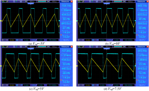
The tests carried out show the transformation of the constant amplitude control signal into a train of switching wave with a frequency and duty cycle dependent on this amplitude. Figure 12 presents the experimental results obtained and Table 2 shows the values of the theoretical and experimental frequencies and duty cycles obtained for the same control voltages.
Table 2. SLDCM output parameters obtained
|
Control voltage |
Output parameters |
||
|
Values |
Frequency (Hz) |
duty cycle |
|
|
-5V |
Theoretical |
888.9 |
0.333 |
|
Experimental |
754.1 |
0.327 |
|
|
0V |
Theoretical |
1000 |
0.500 |
|
Experimental |
843.1 |
0.508 |
|
|
7.5V |
Theoretical |
750 |
0.750 |
|
Experimental |
595.9 |
0.765 |
|
For Vref=-5V, we experimentally obtain a modulated signal of frequency 754.1Hz with a duty-cycle of 0.327, whereas theoretically we have obtained a modulated signal of frequency 888.9Hz with a duty-cycle of 0.333. For Vref=0V, we experimentally obtain a modulated signal of frequency 843.1Hz with a duty-cycle of 0.508, whereas theoretically we have obtained a modulated signal of frequency1000Hz with a duty-cycle of 0.5. For Vref=5V, the modulated signal obtained is symmetrical to that obtained in the case of Vref=-5V. The two modulated signals have approximately the same frequency and the sum of their duty cycle gives 1. For Vref=7.5V, we experimentally obtain a modulated signal of frequency 595.9Hz with a duty-cycle of 0.765, whereas theoretically we have obtained a modulated signal of frequency 750Hz with a duty-cycle of 0.75. The observed differences between the theoretical and experimental values of the frequency of the modulated signal are mainly explained by the fact that the period depends on the values of the passive components. With regard to the duty cycle, the differences between the theoretical and experimental values are much smaller due to the non-dependence of the latter on the values of the passive components. Nevertheless, these minor differences can be explained by the fact that the duty cycle depends on the values of the saturation voltages of the operational amplifier which, experimentally, are +14.6V and -14.6V.
Figure 12. SLDCM output voltages for fixed amplitude control voltages
This work proposes two new duty-cycle modulator structures namely symmetrical linear duty-cycle modulation and general linear duty-cycle modulation. Their principle is based on a double time modulation; both frequency and duty cycle are modulated according to a reference control voltage. These systems have been implemented and observed under different conditions, then compared to the PWM and NIDCM modulators. From the analysis of the results obtained in simulation, several facts can be observed. The variation of the duty cycle is linear while that of the frequency is parabolic. The duty cycle is independent of the values of the passive components used for an analogic modulator, when it is not the case for PWM and NIDCM structures. In addition, it is possible to use a control voltage in [-Vsat; +Vsat] for the SLDCM and in [-Vsat; 0] or [0; +Vsat] for the GLDCM, which allows maximum resolution of the control voltage and flexibility in the control setup, as long as it’s not for PWM and NIDCM structures. According to the experimental results obtained, we note a good similarity between the theoretical and practical duty cycles for the same control signal values. Future work should study digital SLDCM and GLDCM, and the use of proposed modulator in different applications.
The authors would like to express their gratitude to LA SALLE higher technical school for its support during the experimental test.
|
ADC |
Analog-to-Digital Conversion |
|
CB-SVPWM |
Carrier Based Space Vector Pulse Width Modulation |
|
DCM |
Duty Cycle Modulation |
|
GLDCM |
General linear Duty Cycle Modulation |
|
LNIDCM |
Linearized Non-Inverter Duty Cycle Modulation |
|
NIDCM |
Non-Inverter Duty Cycle Modulation |
|
PWM |
Pulse Wave Modulation |
|
SDM |
Sigma Delta Modulation |
|
SLDCM |
Symmetrical linear Duty Cycle Modulation |
|
SPWM |
Sinusoidal Pulse Wave Modulation |
|
THD |
Total Harmonic Distortion |
|
Vref |
Reference or control voltage |
|
Vsat |
Saturation voltage |
|
Vs |
Output voltage |
|
Vo |
Integrator output voltage |
|
Vc |
Capacitor voltage |
|
Greek symbols |
|
|
$\alpha$ |
Duty cycle |
[1] Meng, X.Y., Meng, Z.Y., Chen, T.W., Dimarogonas, D.V., Johansson, K.H. (2016). Pulse width modulation for multi-agent systems. Automatica, 70: 173-178. https://doi.org/10.1016/j.automatica.2016.03.012
[2] Janssen, E., Roermund, A.V. (2011). Basics of sigma-delta modulation. In Look-Ahead Based Sigma-Delta Modulation. Springer, Dordrecht, pp. 5-28. https://doi.org/10.1007/978-94-007-1387-1_2
[3] de la Rosa, J.M. (2011). Sigma-delta modulators: Tutorial overview, design guide, and state-of-the-art survey. IEEE Transactions on Circuits and Systems I: Regular Papers, 58(1): 1-21. https://doi.org/10.1109/TCSI.2010.2097652
[4] Goodman, D.J. (1969). The application of delta modulation to analog-to-PCM Encoding. The Bell System Technical Journal, 48(2): 321-343. https://doi.org/10.1002/j.1538-7305.1969.tb01118.x
[5] Jayant, N.S. (1976). Waveform Quantization and Coding. New York: IEEE Press.
[6] Hauser, M.W. (1991). Principles of oversampling A/D conversion. JAES, 39(1/2): 3-26.
[7] Schreier, R., Pavan, S., Temes, G.C. (2017). Understanding Delta-Sigma Data Converters. Hoboken, NJ, USA: John Wiley & Sons, Inc.
[8] Nneme, L., Lonla, B., Sonfack, G., Mbihi, J. (2018). Review of a multipurpose duty-cycle modulation technology in electrical and electronics engineering. Journal of Electrical Engineering, Electronics, Control and Computer Science, 4(2): 9-18.
[9] Sun, J. (2012). Pulse-Width Modulation. In Dynamics and Control of Switched Electronic Systems, F. Vasca and L. Iannelli, Eds. London: Springer London, pp. 25-61.
[10] Peddapelli, S.K. (2016). Pulse Width Modulation: Analysis and Performance in Multilevel Inverters. Berlin, Boston: De Gruyter Oldenbourg.
[11] Bahena, A.V De León Aldaco, S.E., Alquicira, J.A. (2020). Simulation for a dual inverter feeding a three-phase open-end winding induction motor: A comparative study of PWM techniques. European Journal of Electrical Engineering, 22(1): 13-21. https://doi.org/10.18280/ejee.220102
[12] Djerboub, K., Allaoui, T., Champenois, G., Denai, M., Habib, C. (2020). Particle swarm optimization trained artificial neural network to control shunt active power filter based on multilevel flying capacitor inverter. European Journal of Electrical Engineering, 22(3): 199-207. https://doi.org/10.18280/ejee.220301
[13] Fapi, C.B.N., Wira, P., Kamta, M., Colicchio, B. (2020). Voltage regulation control with adaptive fuzzy logic for a stand-alone photovoltaic system. European Journal of Electrical Engineering, 22(2): 145-152. https://doi.org/10.18280/ejee.220208
[14] Aktaibi, A., Rahman, M.A., Razali, A. (2010). A critical review of modulation techniques. The 19th Annual Newfoundland Electrical and Computer Eng. Conference (NECEC 2010).
[15] Hobraiche, J., Vilain, J.P., Chemin, M. (2004). A comparison between pulse width modulation strategies in terms of power losses in a three-phased inverter-application to a starter generator. Accessed at http://www.utc.fr/lec/Publications/2004/epe_jh.pdf.
[16] Bierhoff, M.H., Fuchs, F.W. (2004). Semiconductor losses in voltage source and current source IGBT converters based on analytical derivation. 2004 IEEE 35th Annual Power Electronics Specialists Conference (IEEE Cat. No.04CH37551), Aachen, Germany, 4: 2836-2842. https://doi.org/10.1109/PESC.2004.1355283
[17] Pattanaik, S.K., Mahapatra, K. (2010). Power loss estimation for PWM and soft-switching inverter using RDCLI. Proceedings of the International Multi Conference of Engineers and Computer Scientists 2010 Vol II, IMECS 2010, Hong Kong.
[18] Cougo, B., Morais, L.M.F., Segond, G., Riva, R., Duc, H.T. (2020). Influence of PWM methods on semiconductor losses and thermal cycling of 15-kVA three-phase SiC inverter for aircraft applications. Electronics, 9(4): 620. https://doi.org/10.3390/electronics9040620
[19] Nneme, L.N., Mbihi, J. (2014). Modeling and simulation of a new duty-cycle modulation scheme for signal transmission systems. American Journal of Electrical and Electronic Engineering, 2(3): 82-87. https://doi.org/10.12691/ajeee-2-3-4
[20] Biard, J.R. (1962). Duty Cycle Modulated Multivibrator, US3037172A.
[21] Mbihi, J., Ndjali, B., Mbouenda, M. (2005). Modelling and simulation of a class of duty-cycle modulators for industrial instrumentation. Iranian Journal of Electrical and Computer Engineering, 4(2): 121-128.
[22] Mbihi, J., Beng, F., Kom, M., Nneme, L. (2012). A Novel Analog-to-digital conversion Technique using nonlinear duty-cycle modulation. International Journal of Electronics and Computer Science Engineering, 7(1): 42-49.
[23] Sonfack, G., Mbihi, J., Moffo, B.L. (2018). Optimal duty-cycle modulation scheme for analog-to-digital conversion systems. International Journal of Electronics and Communication Engineering, 11(3): 354-360.https://doi.org/10.5281/zenodo.1315523
[24] Moffo, B.L., Mbihi, J., Nneme, L.M., Kom, M. (2013). A novel digital-to-analog conversion technique using duty-cycle modulation. International Journal of Circuits, Systems and Signal Processing, 7(1): 42-49.
[25] Mbihi, J., Nneme, L. (2013). A novel control scheme for buck power converters using duty-cycle modulation. Int. J. of Power Electronics, 5(3/4): 185-199. https://doi.org/10.1504/IJPELEC.2013.057038
[26] Sounsoumou, Y., Paulin, Y., Mbihi, J., Djalo, H., Joseph, E. (2018). Virtual digital control scheme for a duty-cycle modulation boost converter, 10(2): 22-27.
[27] Nna, T.P.N., Essiane, S.N., Ngoffé, S.P. (2020). Control of an active filter by duty cycle modulation (DCM) for the harmonic decontamination of a three-phase electrical network. Journal of Power and Energy Engineering, 8(7): 1-14. https://doi.org/10.4236/jpee.2020.87001
[28] Nguefack, L.T., Pauné, F., Kenfack, G.W., Mbihi, J. (2020). A novel optical fiber transmission system using duty-cycle modulation and application to ECG Signal: Analog design and simulation. Journal of Electrical Engineering, Electronics, Control and Computer Science, 6(3).