Rusul Ahmed Shakir* | Marwan T. Mezher | Robert Geber
© 2022 IIETA. This article is published by IIETA and is licensed under the CC BY 4.0 license (http://creativecommons.org/licenses/by/4.0/).
OPEN ACCESS
The present work includes preparation and characterization of polycrystalline complex compounds thin films of (Pb1-zErz)(Zr0.52Ti0.48)1-(z/4)O3 with different erbium concentration (z = 0.05, 0.07, 0.09). Thin films were deposited on nickel /cupper foil substrate by using radio frequency magnetron sputtering technique. Due to the high melting point of ceramic materials, radio frequency magnetron sputtering technique that is employed in the current investigation considers the optimum method compared to other evaporation methods. In order to allow the crystallization into the perovskite phase, the deposited thin films were annealed at 600 ᵒC using the vacuumed furnace. X-Ray diffraction (XRD) and atomic force microscopy (AFM) were employed to characterize the prepared thin films at room temperature. LCR meter was used to determine the dielectric properties at different temperatures and frequencies. The dielectric constant of prepared thin films was at the range of (372-116), while that of loss tangent was about (0.057-0.011). The results show that the values of dielectric constant increase with increasing the temperature and then suddenly decreased as a result of face transformation in Curie temperature, while the values of loss tangent decreased with an increase in frequency. Moreover, the results showed that the dielectric constant, loss tangent and Curie temperature values were decreased with increasing of the erbium content.
radio frequency magnetron sputtering, thin films, PZT, dielectric constant, curie temperature
PZT has been widely focused in researches and extensively adopted by the industry for using in more applications due to its excellent characteristics such as radiation hardness, resistivity and high value of Curie point and remnant polarization [1]. The effects of introducing a variety of dopants in PZT have been studied and reported in the literatures. The effect of adding some rare earth elements to the PZT system is mainly to increase resistivity and reducing the Curie temperature [2].
There are many ways of preparing thin films such as sol-gel process [3], pulsed laser deposition [4], sputtering [5] and chemical vapour deposition [6]. Many studies have been conducted on the rare earth doping of PZT thin films by employing different techniques. Yu et al. [7] they used sol-gel method in order to fabrication of erbium doped PZT thin film with 450 nm thickness on silicon substrate. The X-ray diffraction result shows the formation of (111)-oriented perovskite structure when pyrolyzed at 450℃. The impedance measurements were used to determine the dielectric properties and reported that the dielectric constant values were 900-1000 and tan δ values were 0.06-0.08 at 1 KHz [7].
The ferroelectric properties were measured using P-E loop and they found that, at 100 Hz the Pr value was 23.5μC/cm2 and the coercive field was 5.5kV/mm. Ramam and Lopez [8] studied the effect of doping PLZT ceramic with neodymium on the dielectric, piezoelectric and ferroelectric characterstics. PLZNT ceramic with composition “(Pb0.0985 La0.015Ndy[Zr0.524Ti0.476]0.99-(y/4)Nb0.005O3)” where y (0, 0.25, 0.5, 0.75 and 1 mol%) fabricated by solid state reaction process. The results indicate that the dielectric constant at room temperature was improved up to 1 mol.% of Nd with decreasing in Curie temperature, while the coercive field and remanent polarization were decreased. d33 and kp piezoelectric properties were enhanced as a result of the existence of two donor cations in structure with rising in Nd percentage.
Ramam and Chandramouli [9] investigated the dielectric and piezoelectric characterizations of Ce3+ doping PLSZNT ceramic with composition “(Pb0.976La0.0 14xCexSr 0.01[Zr0.57Ti0.43](0.9975-((0.014-x)/4)-(x/4)) Nb 0.002O3)” for (0 ≤ x ≤ 1 mol.%). The XRD findings revealed that there is a formation of a single rhombohedral structural phase. Also, they measured the dielectric properties at room temperature and reported that the dielectric constant was raised up to 0.6 mol.% of Ce content, while the dielectric loss factor was significantly decreased. Moreover, the results revealed that the optimum piezoelectric characterizations were found when the Ce content was 0.6 mol.%. Pandey et al. [10] synthsized the samarium doped PZT with composition “(Pb1-xSmx(Zr0.65Ti0.35)O3” where x= 0, 0.02, 0.04 and 0.06 by solid state method. A structural property was studied by the XRD technique and the result showed the formation of single phase rhompohedral structure was at x up to 0.04. Also, they studied dielectric properties and noticed that the dielectric constant at room temperature increased and loss factor reduced when the samarium substitution was increased, moreover, the findings showed that the dielectric constant and loss factor values for all samples were decreased after poling.
Shannigrahi et al. [11] studied the dielectric and structural characteristics of PNZT ceramic pellets that prepared from ferroelectric fine powders with composition “Pb1-zNdz(Zr0.60Ti0.40)1-z/ 4O3” where z= 0.07, 0.08 and 0.1 by using sol-gel method. By employing XRD analysis, they reported that the formation of tetragonal system with negligibly small pyroclore structure about 2% was at 550℃. As well, they investigated the dielectric properties at different frequencies (103, 104 and 105) Hz and noticed the dielectric constant was increased with rising in Nd percentage (z). Ramam K and Lopez [12] investigated the effect of doping PLZTN ceramic with strontium on dielectric, piezoelectric and ferroelectric characterization. They used the solid-state reaction process for fabricating of PLSZTN ceramic with composition “[Pb1-x-yLaxSry][(ZrzTi1-z)(1-(x/4)-(5/4)k)Nbk]O3” where y (0, 0.5, 1.0, 1.5 mol.%). The findings showed that the substitution of Sr2+ at pb-site in perovskite structure was resulted in the increasing of the dielectric constant to 2384 and decreased the curie temperature. Moreover, the remanent and spontaneous polarization were increased when the presence of Sr2+ was increased up to 1.5 mol.%. Other paper used RF magnetron sputtering process to manufacture thin films for coated AA2024-T4 [13].
In this paper, the preparation and characterization of erbium doped PZT thin films using R.F magnetron sputtering technique were investigated. The thin films were deposited on Ni/Cu foil substrate with ZrO2 as a buffer layer between the dielectric and substrate. Copper and nickel are a cheap, mechanically compliant, and highly electrically conductive substrate these advantages make them an attractive substrate on which to deposit the PZT thin film [14]. Furthermore, for the annealing process, copper and nickel with their high melting points can withstand 600℃ better than other metals.
Because of Nickel have a good electrical conductive property, high oxidation resistance, a high melting point in contrast with the aluminium electrode, also the thermal expansion coefficient near the thermal expansion coefficient of ceramic when compared with other metals. The aforementioned properties make the nickel is suitable for using as capacitor electrode. Copper foil is an inexpensive, flexible substrate with good electrical conductivity which render it an ideal for many capacitor applications.
2.1 Preparation of PEZT compound
The materials such as lead acetate trihydrate Pb(CH3COO)2∙3H2O, erbium acetate tetrahydrate (CH3COO)3Er∙4H2O, zirconium isopropoxide Zr(C3H7O)4, and titanium isopropoxide Ti[(CH3)2CHO]4 were employed to manufacture the polycrystalline sputtering targets of PEZT. In order to obtain a monolithic gel, the ethylene glycol was employed as an additive to prevent the cracking and improving the surface smoothness, while the distilled water and glacial acetic acid were used as solvents. For preparation the compound, the erbium acetate and lead acetate were separately dissolved in the acetic acid as shown in Figure 1.
Throughout the stirring, titanium isopropoxide and zirconium isopropoxide were added to the mixture, respectively. When the initial reaction has been completed, the ethylene glycol was added. The condensed solid was formed by alcolyzed the residual titanium isopropoxide and zirconium isopropoxide with ethylene. For the sake of obtaining the final sol, a little quantity of distilled water was gradually poured to the solution.
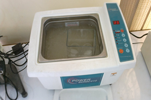
Figure 1. The prepared solution in sonication device
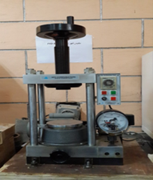
The produced sol was then heated to 50℃ for 24 hours to form a transparent gel. Later, the transparent gel was dried at 100℃ for 72 hours and calcined at 550℃ for 10 hours. The obtained PEZT powder was mixed with the PVA binder and cold-pressed into discs with (50 mm diameter X 3-4 mm thickness), at the pressure of 6 tons by using an electrical hydraulic press for 3 min forming time. The formed targets were dehydrated at 50℃ for 30 min in an electrical oven to evaporate the PVA solution binder. According to the target holder dimensions in the radio frequency magnetron sputtering system, the size of the target should be 50 mm as a diameter and (3-4 mm) as a thickness. Therefore, the target was heated up to this temperature to increase the target rigidity. Nickel and zirconia micro powder were weighted and pressed as a disc with (50 mm diameter X 5 mm thickness) by using an electrical hydraulic press at 10 tons for nickel and 8 tons for zirconia. The forming time was 4 min in a cylindrical steel die, Figure 2 shows the electrical hydraulic press.
Figure 2. The electrical hydraulic press
2.2 Preparation of PEZT thin films
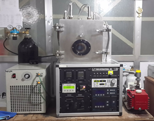
PEZT targets were used in precipitation of the dielectric layer. Ni/Cu foil substrates were synthesised through using the R.F. Magnetron sputtering deposition of Ni on copper foil was achieved in argon as sputtering gas. In order to ensure the dielectric properties, ZrO2 was selected as a buffer layer between the dielectric thin film and the metal electrode. ZrO2 layer acts both as adhesion layer between the PZT or PSZT dielectric layer and Ni bottom electrode, and to prevent attack of the Ni layer by any oxygen formed during sputtering deposition of the dielectric films. Also ZrO2 acts as matching layer between the thermal expansion coefficient of the PZT or PSZT dielectric and the substrate. The PEZT dielectric thin film was deposited by R.F. Magnetron sputtering system on Ni/Cu foil substrate with ZrO2 buffer layer, Figure 3 shows the R.F magnetron sputtering deposition system. Table 1 shows the sputtering deposition conditions of Ni, ZrO2 and dielectric thin film.
Figure 3. R.F. Magnetron sputtering technique system
Table 1. The sputtering deposition conditions of Ni, ZrO2 and dielectric thin film
|
Parameter |
Ni film deposition |
ZrO2 film deposition |
PEZT film deposition |
|
Ar+ pressure (Torr) |
2.5*10-2 |
4.8*10-2 |
2*10-2 |
|
Power (W) |
200 |
50 |
80 |
|
REF (W) |
4 |
0 |
1 |
|
Substrate rotational Speed (cycle/min.) |
4 |
4 |
4 |
|
Deposition angle (°) |
55° |
55° |
55° |
|
Deposition time (min) |
16 |
40 |
300 |
|
Layer thickness (nm) |
200 |
10 |
900 |
|
Distance between target and substrate (cm) |
10 |
10 |
10 |
Figure 4. The deposited thin films
PbO layer was spin-coated on the surface of PEZT thin films to prevent the Pb deficient after the sputtering process. PbO solution was spin coated on the films by using spin coating machine at 3000 rpm for 30 s, Figure 4 shows the samples of deposited thin films. Based on the preliminary experiments, it was found that this time is better for obtaining very thin film with a good homogeneity.
2.3 Annealing technique
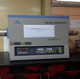
In order to allow the crystallization into the perovskite phase, the amorphous deposited thin films were subjected to the heat treatment in vacuumed furnace with a heating rate of 3℃/min up to 600℃ with soaking time 30 min and later slowly cooled down until reached to the room temperature, Figure 5 illustrates the vacuumed furnace.
Figure 5. The vacuumed furnace
2.4 Structural and electrical characterization
Phase and crystalline structure analyses were performed with aid of using the X-ray diffractometer (copper Kα radiation, the wavelength λ= 1.5405 A°), Figure 6 shows the specimen inside the X-ray diffractometer.
Figure 6. The specimen inside the X-ray diffractometer
Surface morphology, roughness and particle size were analysed by using the atomic force microscopy (AFM, SPM-AA3000, Angstrom Advanced INC., USA). LCR meter was employed to measure the dielectric properties in the evacuated condition as depicted in Figure 7. In order to create the top electrode, the nickel was sputtered on the surface of PEZT thin film layer by using the magnetron sputtering technique. The capacitance and resistance values were evaluated at various temperatures and frequencies (1, 10 and 100 kHz), Figure 8 shows a schematic sketch for multilayer deposited thin films.
Figure 7. LCR meter
Figure 8. Schematic figure represents deposited thin films
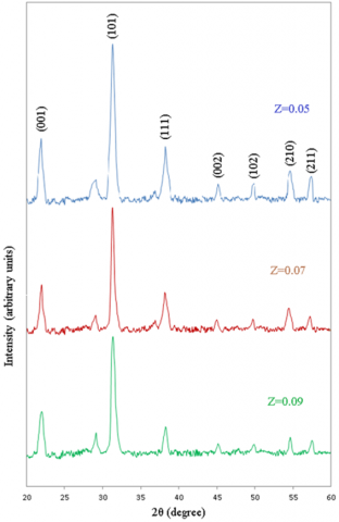
The results showed that the dominant phase after the annealing process at 600℃ is the perovskite phase at 2θ = 22°, 31.357°, 38.25°, 45.15°, 49.9°, 54.68°, and 57.45° as shown in Figure 9 below. Although, there is a little shift in the peak positions, the XRD findings indicate that the basic crystal structure of the PZT is unchanged by the substitution of erbium ions (Er3+). The observed shifting refers that there is a little variation happened in the lattice parameters. Moreover, The XRD results showed the presence of some peaks for non-equilibrium oxides, these oxides rabidly begin to decompose at higher annealing temperature or due to the presence of some impurities in raw materials.
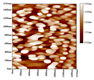
As it evident from Figures 10 and 11, the AFM results show that the surface of deposited thin films is a dense and a homogenous with a uniform grain size distribution; the uniformity of grain size was increased when the erbium content were increased. Furthermore, the figures showed that the grain size was in nano structure and there are no cracks was noticed at the surface. The grain size of the produced film was decreased with the addition of eribum to the PZT structure.
Figure 9. Comparison of XRD results of PEZT
Figure 10. The surface morphology of pure PZT thin film
Figure 11. The surface morphology of erbium doped PZT thin film
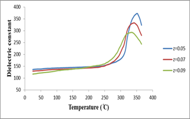
The results of dielectric properties measurement as shown in Figure 12 shows that the values of dielectric constant initially were increased with the increasing in temperature and then suddenly reduced at a temperature that so-called called Curie temperature. The decreasing in dielectric constant created as a result of transition from ferroelectric to para-electric at Curie temperature of about (351, 343 and 335℃) for (0.05, 0.07 and 0.09 %Er), respectively. The PZT is a ferroelectric material that has perovskite structure at a wide range of temperatures. Perovskite is a tetragonal phase, for this phase the center of the positive and negative charges do not coincide, so the dipoles were formed with this structure. When the temperature raising up to transition temperature the structure of the material is deformed and transferred from the tetragonal (perovskite) phase to the more cubic phase. The center of positive and negative charges of cubic phase is more coinciding, so the dipoles disappear and the dielectric constant decreased [15, 16]. During the doping process, the erbium ions will enter the perovskite structure of PZT, causing the deformation for that structure and leading to the variation in the Curie temperature.
Figure 12. The effect of temperature on dielectric constant
Figure 13. The effect of frequency on dielectric constant
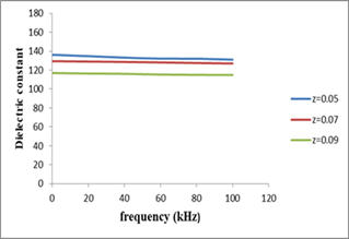
Figures 13 and 14 show that the value of loss tangent decreases with increasing of the applied frequency, despite the impact of dielectric constant was very small. As the frequency increased, the materials net polarization decreases because the rearrangement of molecules by the effect of heat and higher frequency, so the dielectric constant decreased. At lower frequency the higher value of dielectric constant is due to simultaneous presence of all type of polarization (space charge, dipole, ionic, electronic, …, etc.) which found to decrease with increasing frequency. At higher frequency (>1012 Hz) electronic polarization only exist.
Figure 14. The effect of frequency on tangent loss of PEZT at room temperature
The dielectric constant of the films was between 372-116, whilst that of loss tangent was about 0.057-0.011, this range in the values due to the variation in composition of the film and the difference of the temperature and frequency. The dielectric constant, loss tangent and curie temperature values were decreased with increasing of the erbium content.
In this study, the preparation of the erbium doped PZT thin films achieved by using the R.F. Magnetron sputtering on Ni/Cu foil substrate with using ZrO2 as a buffer layer. The following conclusions from this work are as follows:
Greek symbols
|
λ |
wavelength |
|
Ɵ |
angle |
|
Subscripts |
|
|
XRD |
x-ray diffraction |
|
AFM |
atomic force microscopy |
|
LCR |
inductance, capacitance, resistance meter |
|
PZT |
Lead zirconate titanate |
|
PEZT |
Lead eribum zirconate titanate |
[1] Haertling, G.H. (1990). Ferroelectric ceramics: History and technology. Journal of the American Ceramic Society, 82(4): 797-818. https://doi.org/10.1111/j.1151-2916.1999.tb01840.x
[2] Pandey, S.K., Kumar, S., Chatterjee, S.N., Kumar, U., Prakash, CH., Chatterjee, R., Goil, T.C. (2007). Growth and characterization of Sm3+ -substituted PZT thin films. Physica B: Condensed Matter, 388(1-2): 404-411. https://doi.org/10.1016/j.physb.2006.06.167
[3] Levy, D., Zayat, M. (2015). The Sol-Gel Handbook- Synthesis, Characterization, and Applications: Synthesis, Characterization and Applications, 3-Volume Set. Wiley-VCH Verlag GmbH and Co. KGaA,
[4] Eason, R. (2007). Pulsed Laser Deposition of Thin Films: Application-LED Growth of Functional Materials. Wiley-Interscience, A John Wiley and Sons, INC., Publication. https://doi.org/10.1002/0470052120
[5] Wasa, K. (2012). 2 - sputtering phenomena. Handbook of Sputter Deposition Technology: Sputtering Phenomena, pp. 42-75. https://doi.org/10.1016/B978-1-4377-3483-6.00002-4
[6] Hugh, O., Pierson, H.O. (1999). 2 - fundamentals of chemical vapor deposition. Handbook of Chemical Vapor Deposition (CVD): Principles, Technology, and Applications, 36-67. https://doi.org/10.1016/B978-081551432-9.50005-X
[7] Yu, Y.J., Chan, H.L.W., Wang, F.P., Li, K., Choy, C.L., Zhao, L.C. (2003). Structural and ferroelectric properties of europium doped lead zirconate titanate thin films by a sol–gel method. Thin Solid Films, 424(2): 161-164. https://doi.org/10.1016/S0040-6090(02)01052-0
[8] Ramam, K., Lopez, M. (2008). Dielectric, ferroelectric and piezoelectric studies of neodymium-modified PLZNT ceramics for sensor and actuator applications. Journal of Alloys and Compounds, 466(1-2): 398-403. https://doi.org/10.1016/j.jallcom.2007.11.055
[9] Ramam, K., Chandramouli, K. (2009). Effect of rare-earth donor Ce3+ doping at A-site of PLSZNT on dielectric and piezoelectric properties. Current Applied Physics, 9(5): 907-912. https://doi.org/10.1016/j.cap.2008.09.005
[10] Pandey, S.K., Thakur, O.P., Bhattacharya, D.K., Prakash, C., Chatterjee, R. (2009). Structural and electrical properties of Sm3+ substituted PZT ceramics. Journal of Alloys and Compounds, 468(1-2): 356-359. https://doi.org/10.1016/j.jallcom.2008.01.006
[11] Shannigrahi, S.R., Choudhary, R.N.P., Acharya, H.N. (1999). Structural and dielectric properties of Nd modified Pb (Zr0.60Ti0.40)O3 ceramics. Materials Science and Engineering: B, 60(1): 31-39. https://doi.org/10.1016/S0921-5107(99)00002-1
[12] Ramam, K., Lopez, M. (2007). Effect of strontium doping on dielectric, ferroelectric and piezoelectric properties of PLZTN ceramics. Materials Science and Engineering B, 145(1-3): 41-47. https://doi.org/10.1016/j.mseb.2007.09.085
[13] Namer, N.S.M., Nama, S.A., Mezher, M.T. (2019). The influence of nano particles additive on tribological properties of AA2024-T4 coated with TiN or SiN thin films. Journal of Mechanical Engineering Research and Developments (JMERD), 42(3): 30-34. https://doi.org/10.26480/jmerd.03.2019.30.34
[14] Gebhardt, S., Seffner, L., Schlenkrich, F., Schonecker, A. (2007). PZT thick films for sensor and actuator applications. Journal of the European Ceramic Society, 27(13-15): 4177-4180. https://doi.org/10.1016/j.jeurceramsoc.2007.02.122
[15] Uchino, K. (2010). Advanced Piezoelectric Materials: Science and Technology. Cambridge, U.K. https://doi.org/10.1533/9781845699758
[16] Jaffe, B., Cook, W. (1971). Piezoelectric Ceramics. Academic Press, London.