OPEN ACCESS
In Conventional full bridge inverters, the output voltage is lower than that of the input DC voltage. Front end step up converters are generally required in applications where the input DC voltage is very low, which leads to two stage conversion process. Single Stage Boost Inverter (SSBI) has many advantages like less number of power devices, simple structure and capable of operating in buck as well as boost modes. The conventional modulation strategy employed in SSBI has many drawbacks such as all the devices operate at higher frequency; the devices should withstand higher voltage and current stress which leads to large conduction and switching losses there by reducing their efficiency. This paper proposes a new modulation strategy, namely, low switching modulation (LSM) where all the devices are made to operate at high frequency only in one half cycles which reduces the conduction and switching losses drastically and thereby increasing the efficiency of SSBI. Moreover to reduce the current circulation losses in SSBI, an improved SSBI is proposed, which can bypass the inductor current with low switching stress. Comparison between the conventional SSBI and LSM modulated SSBI are detailed with analysis is discussed in this paper. The proposed SSBI and its modulation techniques are simulated in the MATLAB/SIMULINK software and the results are also presented.
single stage boost inverter (SSBI), low switching modulation (LSM), voltage stress, current stress
To realize a DC-AC conversion, a full bridge inverter topology is mostly used. This full bridge inverter is a buck inverter, where the load voltage will be always lesser when compared to the input DC voltage. In certain applications (like PV, UPS etc), an additional front end DC-DC converter is required to step up the low DC voltage. This increases number of conversion stages to two (i.e. DC-DC & DC-AC), which makes the system more complex, increases the number of switching devices and thereby reducing the efficiency because of two stages of conversion.
Instead of DC-DC converter at the front end, a step up transformer can be used at the load side to increase the AC voltage fed to the load. This increases the size and cost of the entire system described by Bose (2010) and Zhao et al. (2011). In order to minimize the number of conversion stages and the power devices used, many single stage boost inverters are proposed by the Caceres & Barbi (1999), Chen & Smedley (2008), Mirafzal et al. (2011), Li & Wolfs (2008), Kjaer et al. (2005) Ilango et al. (2010). A Z-source inverter, also known as quasi-single-stage inverter, is capable of boosting up the voltage, by allowing shoot through states in the legs of the inverter shown in Yang & Liang (2012). Even though the Z source inverter is capable of boosting up the load voltage, it suffers from drawbacks like capacitor voltage stress and huge inrush current which will reduce the efficiency. Further the number of passive components used in Z source inverter is more which increases the size and cost. A novel active buck boost inverter is proposed in Zhou & Huang (2012) which can step up the load voltage and can be operated in both buck and boost mode, but the main drawback of this proposal is number of power devices used is increased.
Single Stage Boost inverter (SSBI) with two bidirectional DC-DC boost converters connected in cascade is proposed by Li et al. (2013). The SSBI proposed by Y. Li, S. Jiang et al. (2013) has two boost converters; whose output voltages are DC biased sinusoidal quantities but out-of phase with each other. The output voltage of SSBI proposed by Li et al. (2013) can be more than the DC input voltage, whose value is dependent on the duty cycle of the two DC-DC converters. The main drawback of the SSBI proposed by Li et al. (2013) is that the load current has low frequency ripples. To eliminate this low frequency ripples in the current waveform, a suitable modulation control strategy is proposed by Tang et al. (2014). To improve the power bandwidth SSBI proposed by Li et al. (2013) a dynamic linearization modulator for buck boost inverter is proposed by Zhou & Huang (2012). Conventional modulation strategy for SSBI as in Li et al. (2013) controls each bidirectional DC-DC converter to produce sinusoidal DC voltage with same DC bias. Nevertheless, all the power electronic devices used in Li et al. (2013), Tang et al. (2014) Zhou & Huang (2012) operate at high frequency and the devices also need to sustain high voltage and current stress. This leads to high conduction and switching losses there by reducing the efficiency of the SSBI. In the interim, the output current will flow through the inductor, whose losses will further decrease the efficiency of SSBI. Gagliano & Nocera (2017) proposes the effective way for electric energy storage in residential applications.
This manuscript proposes a Low Switching Modulation (LSM) strategy, which makes one boost converter to operate during the positive half cycle of the reference wave and other boost converter to operate during the negative half cycle of the reference wave with same DC bias. The load receives a pure sinusoidal voltage, which is the difference between the outputs of two DC-DC boost converters. The main advantage of the proposed LSM technique is that it reduces the number of power devices working at high frequency, further reduces the voltage and current stress of the switches and the inductors. This in turn reduces the switching and conduction losses of the switches, core losses and copper losses of the inductor are also reduced. Moreover to reduce the current circulation losses in SSBI, an improved SSBI with two additional switches for clamping is introduced, which is also modulated using LSM. The improved SSBI has higher efficiency and lower voltage stress when compared to the conventional SSBI.
The rest of the manuscript is organized as follows: In section 2 SSBI controlled by LSM is detailed along with its modes of operation. Section 3 introduces the improved SSBI under LSM and its modes of operation are also explained in detail. Simulation results are discussed in section 4 and Section 5 concludes the work.
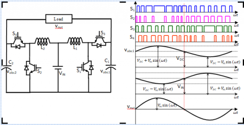
The conventional SSBI is shown in Figure 1(a) and the conventional modulation scheme waveforms proposed by Li et al. (2013) is shown in Figure 1(b). From Figure 1(b) the output voltage waveform of the DC-DC boost converter is sinusoidal quantity with same DC bias. Further in the conventional modulation scheme all the power electronic devices are operated at high frequency.
Figure 1. Conventional modulation strategy and waveforms (a) conventional SSBI topology (b) conventional modulation scheme
Now let us define the $v _ { o b c 1 }$ and $v _ { o b c 2 }$ be the output voltages of the capacitors of boost converter 1 and boost converter 2 respectively, which is given by,
$v _ { o b c 1 } = V _ { D C } + \frac { 1 } { 2 } V _ { m } \sin ( \omega t )$ (1)
$v _ { o b c 2 } = V _ { D C } + \frac { 1 } { 2 } V _ { m } \sin ( \omega t - \pi )$ (2)
Where VDC is the offset DC voltage and Vm is the maximum value of the load voltage. The load voltage can be expressed in terms of the capacitor voltages $v _ { o b c 1 }$ and $v _ { o b c 2 }$ as given below,
$v _ { \text {load} } ( t ) = v _ { o b c 1 } ( t ) - v _ { o b c 2 } ( t ) = \frac { V _ { I N } } { 1 - d _ { 1 } ( t ) } - \frac { V _ { I N } } { 1 - d _ { 2 } ( t ) }$ (3)
Where d1 (t) and d2 (t) are the duty cycles of the switches S1 and S2 respectively. Further $V _ { D C } \geq V _ { I N } + \frac { V _ { m } } { 2 }$, from the above equation (1), (2) and (3) we can derive,
$d _ { 1 } ( t ) = \frac { \frac { V _ { m } } { 2 } + \frac { V m } { 2 } \sin ( \omega t ) } { V _ { I N } + \frac { V m } { 2 } + \frac { V m } { 2 } \sin ( \omega t ) }$ (4)
$d _ { 2 } ( t ) = \frac { \frac { V _ { m } } { 2 } - \frac { V _ { m } } { 2 } \sin ( \omega t ) } { V _ { I N } + \frac { V _ { m } } { 2 } - \frac { V _ { m } } { 2 } \sin ( \omega t ) }$ (5)
From equations (1) to (5) we can derive the expression for load voltage as,
$v _ { \text {load} } ( t ) = v _ { \text {obc1} } ( t ) - v _ { \text {obc2} } ( t ) = V _ { m } \sin ( \omega t )$ (6)
The waveforms of $v _ { o b c 1 } , v _ { o b c 2 }$ and $v _ { l o a d }$ are shown in Figure 1(b). The voltages $v _ { o b c 1 }$ and $v _ { o b c 2 }$ are sinusoidal with DC bias. The load voltage $v _ { l o a d }$ is pure sinusoidal which is the difference between $v _ { o b c 1 }$ and $v _ { o b c 2 }$.
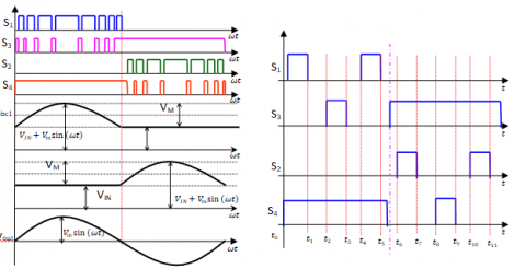
Figure 2(a) shows the proposed LSM scheme. From the figure, switches S1 and S3 are switched at high frequency during the positive half cycle of the load voltage and are complementary to each other. During this instant switch S2 is turned ON whereas switch S4 is turned OFF. Further the switches S2 and S4 are switched at high frequency during the negative half cycle of the load voltage and are complementary to each other. During this instant switch S3 is turned ON whereas switch S1 is turned OFF. The capacitance voltages$v _ { o b c 1 }$ and $v _ { o b c 2 }$ using the LSM scheme for both the half cycles is given in equations (7) and (8). Figure 2(b) shows the control scheme of LSM technique.
$\left\{ \begin{array} { c } { v _ { o b c 1 } ( t ) = V _ { m } \sin ( \omega t ) + V _ { I N } } \\ { v _ { o b c 2 } ( t ) = V _ { I N } } \end{array} \right.$ (7)
$\left\{ \begin{array} { c } { v _ { o b c 1 } ( t ) = V _ { I N } } \\ { v _ { o b c 2 } ( t ) = V _ { m } \sin ( \omega t - \pi ) + V _ { I N } } \end{array} \right.$ (8)
$v _ { \text {load} } ( t ) = v _ { o b c 1 } ( t ) - v _ { o b c 2 } ( t ) = \frac { V _ { I N } } { 1 - d ( t ) } - V _ { I N }$ (9)
From equations (7)–(9) we can derive,
$d ( t ) = \frac { V _ { m } \sin ( \omega t ) } { V _ { I N } + V _ { m } \sin ( \omega t ) }$ (10)
Where d(t) is the duty cycle of the switches S1 and S2. The load voltage can be derived by calculating the difference in voltage between $v _ { o b c 1 }$ and $v _ { o b c 2 }$
$v _ { l o a d } ( t ) = v _ { o b c 1 } ( t ) - v _ { o b c 2 } ( t ) = \frac { V _ { I N } } { 1 - d ( t ) } - V _ { I N } = V _ { m } \sin ( \omega t )$ (11)
Figure 2. Low switching modulation (LSM) techniques (a) key waveforms (b) control scheme of LSM
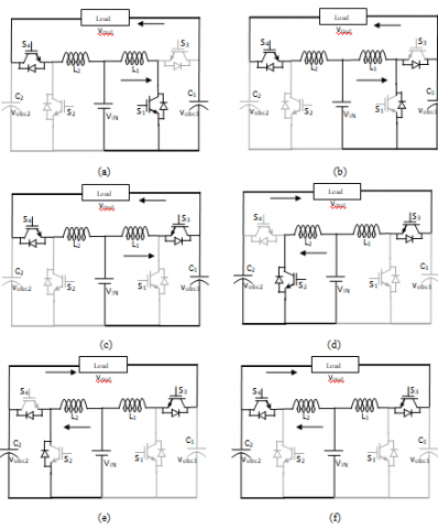
Figure 3. Modes of operation (a) [t0, t1], (b) [t1, t2] or [t3, t4], (c) [t2, t3], (d) [t6, t7], (e) [t7, t8] or [t9, t10], and (f) [t10, t11]
In a switching cycle, the converter under LSM has four switching modes. Figure 2(b) shows the control scheme of LSM, and Figure 3 shows the equivalent circuits of the switching modes in the switching cycle. Before the following analysis, the following are some assumptions: 1) all the switches and diodes are ideal; 2) all the capacitors and inductors are ideal; and 3) C1=C2, L1=L2.In the period that the output voltage is positive:
1) Mode 1 [t0, t1]: At t0, S1, S4 are turned on, the input voltage is applied on L1, and the input current charges L1. Load current io flows through S4 (D4) to VIN, which is supplied by C1, as shown in Figure 3(a).
2) Mode 2 [t1, t2]: The period is dead time. At t1, S1, S2, and S3 are turned off, S4 is turned on, and the current iL1 flows through D3 or D1 (according to the current direction), as shown in Figure 3(b). Load current ioflows through S4 (D4) to VIN.
3) Mode 3 [t2, t3]: At t2, S3 is turned on and iL1 flows through S3 (D3). Load current ioflows through S4 (D4) to Vin. The current-flow path is shown in Figure 3(c).
4) Mode 4 [t3, t4]: The period is also dead time, and the operating mode is the same as that of mode 2.
In the period that the output voltage is negative:5) Mode 5 [t6, t7]: At t6, S2, S3 are turned on, the input voltage is applied on L2, and the input current charges L2. Load current ioflows through S3 (D3) to VIN, which is supplied by C2, as shown in Figure 3(d).
6) Mode 6 [t7, t8]: The period is dead time. At t7, S1, S2, and S4 are turned off, S3 is turned on, and the current iL2 flows through D4 or D2 (according to the current direction), as shown in Figure 3(e). Load current ioflows through S3 (D3) to VIN.
7) Mode 7 [t8, t9]: At t8, S4 is turned on and iL2 flows through S4 (D4). Load current ioflows through S3 (D3) to VIN. The current-flow path is shown in Figure 3(f).
8) Mode 8 [t9, t10]: The period is also dead time, and the operating mode is the same as that of mode 6.
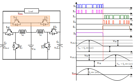
Whether traditional modulation method or LSM strategy is utilized, current circulation of the converter still exists, which means the core loss and the copper loss of inductors L1, L2 will exist all the time. In half line cycle, only one inductor is needed to play a booster role under LSM strategy; the other output side can be clamping to VIN by using a clamping switch. The clamping switches operate in line frequency, and the voltage stress is much lower. For low-voltage-stress applications, low cost MOSFET can be utilized, which means the conduction loss is lower than IGBT in the same condition; therefore, low-cost MOSFETs can be applied. The topology is shown in Figure 4(a), 4(b) shows the modulation strategy and the key waveforms. The switching mode of the converter with clamping switches is similar to LSM. In the period that the output voltage is positive, S4 is turned off, voltage of C2 is clamped to VIN by clamping switch S6, and the load current io flows through S6 to Vin, which is supplied by C1. In the period that the output voltage is negative, S3 is turned off; voltage of C1 is clamped to VIN by clamping switch S5, and the load current io flows through S5 to VIN, which is supplied by C2. Figure 10 shows the control logic under LSM with clamping switches. Figure 5 shows the detail modes of the improved converter with clamping switches. The converter with clamping switch mode is the same as the mode under LSM. The voltage/current stress is the same as LSM, except clamping switches. The current stress of clamping switch is io, and the voltage stress of clamping switch is (Vload–VIN), which is lower than both of conventional method and LSM. The clamping switches obviously have a further lower voltage stress, leading to a lower conduction loss. Moreover, clamping switches reduce the inductor core loss and copper loss generated by circulation current.
Figure 4. Improved modulation strategy and waveforms (a) improved SSBI topology (b) modulation scheme
Figure 5. Modes of operation of improved SSBI
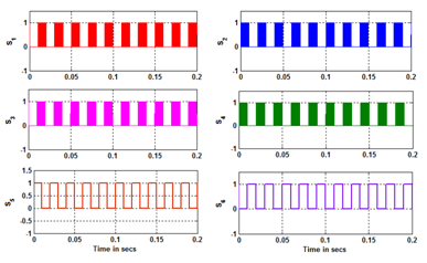
To verify the validity of the proposed low switching modulation scheme, the proposed SSBI with LSM is simulated using MATLAB/SIMULINK. The simulation results are presented in this section. The simulation parameters used in this study is given in table (i). Figure 6 shows the switching signals of all the four switches generated via LSM scheme which is fed into the switches of conventional SSBI. It is evident from the Figure 6 that all the switches operate at high frequency only in one half cycle period. The duty cycle under consideration is 0.8.
Table 1. Simulation parameters
|
Parameter |
Value |
|
Input voltage |
80 V |
|
Output voltage |
110 V |
|
Fundamental Frequency |
50 Hz |
|
Switching frequency |
20 kHz |
|
Inductance |
500 μH |
|
Capacitance |
20 μF |
Figure 6. Switching signals of LSM fed to conventional SSBI
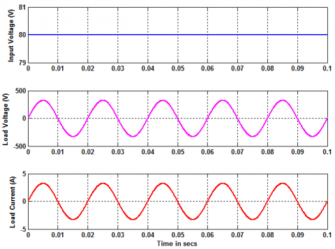
Figure 7 shows the input DC voltage fed in to the conventional SSBI modulated through LSM (which is 80V DC). Further the Figure 7 also shows the load voltage and load current waveforms of the conventional SSBI. It is clear from that the load voltage is sinusoidal and load current is also sinusoidal. The load voltage RMS value can be controlled by controlling the duty cycle of the switches. Here in this case the duty cycle is considered as 0.8. Increasing or decreasing the duty cycle increases or decreases the load voltage accordingly.
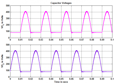
Figure 8 shows the capacitor voltage of the conventional SSBI modulated via LSM scheme of modulation. In this case capacitor voltages follow a sinusoidal quantity for one half cycle, where as in the next half cycle the capacitor voltage is maintained at a value equal to the DC input voltage. The two capacitor voltages are complemented to each other in maintaining the DC input voltages.
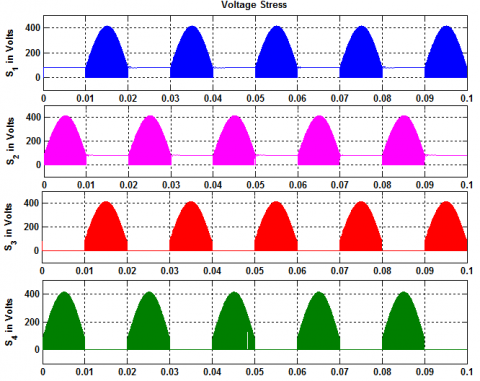
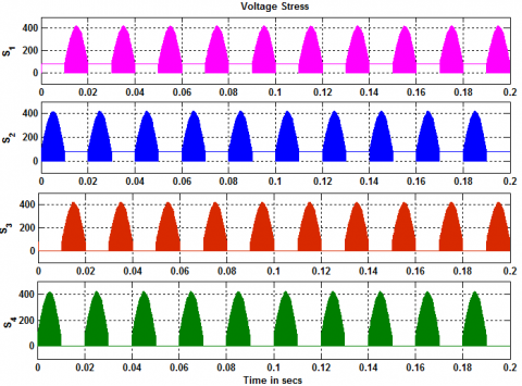
Figure 9 shows the voltage stress across the switches S1, S2, S3 and S4. The switching stresses of the devices are much higher which leads to the development of the improved SSBI which is shown in 4. Further the same LSM scheme is used to trigger the switches of improved SSBI and their results are also presented.
Figure 7. Input DC voltage, load voltage and load current of LSM fed to conventional SSBI
Figure 8. Capacitor voltages of LSM fed to conventional SSBI
Figure 9. Voltage stress of switching devices using LSM in conventional SSBI
Figure 10. Switching signals of LSM fed to improved SSBI
Figure 11. Input DC voltage, load voltage and load current of LSM fed to improved SSBI
Figure 12. Voltage stress of switching devices using LSM in improved SSBI
Figure 10 shows the switching signals of the LSM fed in to improved SSBI. From figure 10 it is evident that the newly added switches switch at fundamental frequency which reduces the switching losses and thereby increasing the efficiency. Figure 11 shows the input DC voltage fed in to the improved SSBI modulated through LSM (which is 80V DC). Further the Figure 7 also shows the load voltage and load current waveforms of the improved SSBI. It is clear from that the load voltage is sinusoidal and load current is also sinusoidal. The load voltage RMS value can be controlled by controlling the duty cycle of the switches. Here in this case the duty cycle is considered as 0.8. Increasing or decreasing the duty cycle increases or decreases the load voltage accordingly. Figure 12 shows the switching stress of the four main switches of the improved SSBI.
This paper proposed an improved SSBI under LSM with clamping switches. According to the analysis and experimental results, the LSM strategy with clamping switches of SSBI keeps the advantage of buck–boost ability. Furthermore, it brings the following advantages over the original one: Only half of the switches are working in high frequency under LSM compared with conventional modulation, which obviously reduces the switching loss of the SSBI. The voltage/current stress of the switches is lower with LSM than conventional modulation, which will further reduce the switching loss and conduction loss of the power switches. The inductor current is lower with LSM, which also reduces the magnetic loss. Clamping switches is helpful to lower the current circulation loss of inductor and IGBT. With low-stress MOSFET, it can also reduce the conduction loss of circulation current. The efficiency of SSBI can be improved with LSM because high-frequency switches is less than traditional modulation, also the inductor current stress is lower; in addition, the improved SSBI can further improve the efficiency because of the low conduction loss by introducing low stress switches.
Bose B. (2010). Global warming: Energy, environmental pollution, and the impact of power electronics. IEEE Trans, Ind, Electron, Mag, Vol. 4, No. 1, pp. 6-17. https://doi.org/10.1109/MIE.2010.935860
Caceres R. O., Barbi I. (1999). A boost DC–AC converter: Analysis, design, and experimentation. IEEE Trans, Power Electron, Vol. 14, No. 1, pp. 134-141. https://doi.org/10.1109/63.737601
Chen Y., Smedley K. (2008). Three-phase boost-type grid-connected inverter. IEEE Trans, Power Electron, Vol. 23, No. 5, pp. 2301-2309. https://doi.org/10.1109/TPEL.2008.2003025
Gagliano A., Nocera F. (2017). Analysis of the performances of electric energy storage in residential applications. International Journal of Heat and Technology, Vol. 35, No. S1, pp. S41-S48. https://doi.org/10.18280/ijht.35Sp0106
Ilango G. S., Potnuru S., Karthikeyan A., Chilakapati N. (2010). Single-stage sine-wave inverter for an autonomous operation of solar photovoltaic energy conversion system. Renew, Energy, Vol. 35, No. 1, pp. 275-282. https://doi.org/10.1016/j.renene.2009.06.009
Jang M., Agelidis V. G. (2011). A minimum power-processing-stagefuel-cell energy system based on a boost-inverter with a bidirectional backup battery storage. IEEE Trans, Power Electron, Vol. 26, No. 5, pp. 1568-1576. https://doi.org/10.1109/APEC.2010.5433655
Kjaer S. B., Pedersen J. K., Blaabjerg F. (2005). A review of single-phase grid-connected inverters for photovoltaic modules. IEEE Trans, Ind, Appl, Vol. 41, No. 5, pp. 1292-1306. https://doi.org/10.1109/TIA.2005.853371
Lai J. S. (2009). Power conditioning circuit topologies. IEEE Ind, Electron, Mag, Vol. 3, No. 2, pp. 24-34. https://doi.org/10.1109/MIE.2009.932580
Li Q., Wolfs P. (2008). A review of the single phase photovoltaic module integrated converter topologies with three different dc link configurations. IEEE Trans, Ind, Electron, Vol. 23, No. 3, pp. 1320-1333. https://doi.org/10.1109/TPEL.2008.920883
Li Y., Jiang S., Cintron-Rivera J. G., Peng F. (2013). Modeling and control of quasi-Z-source inverter for distributed generation applications. IEEE Trans, Power Electron, Vol. 60, No. 4, pp. 1532-1541. https://doi.org/10.1109/TIE.2012.2213551
Mirafzal B., Saghaleini M., Kaviani A. K. (2011). An SVPWM based switching pattern for stand-alone and grid-connected three-phase single stage boost inverters. IEEE Trans, Power Electron, Vol. 26, No. 4, pp. 1102-1111. https://doi.org/10.1109/TPEL.2010.2089806
Tang Y., Dong X. M., He Y. H. (2014). Active buck–boost inverter. IEEE Trans, Power Electron, Vol. 60, No. 8, pp. 4691-4697. https://doi.org/10.1109/TIE.2013.2293694
Yang L. S., Liang T. J. (2012). Analysis and implementation of a novel bidirectional DC–DC converter. IEEE Trans, Ind, Electron, Vol. 59, No. 1, pp. 422-434. https://doi.org/10.1109/TIE.2011.2134060
Zhao W., Lu D. D. C., Agelidis V. G. (2011). Current control of grid-connected boost inverter with zero steady-state error. IEEE Trans, Power Electron, Vol. 26, No. 10, pp. 2825-2832. https://doi.org/10.1109/TPEL.2011.2128349
Zhou T. F., Huang W. X. (2012). Single-stage boost inverter with coupled inductor. IEEE Trans, Ind, Electron, Vol. 27, No. 4, pp. 1885-1893. https://doi.org/10.1109/TPEL.2011.2165855
Zhou Y., Huang W. (2012). Single-stage boost inverter with coupled inductor. IEEE Trans, Power Electron, Vol. 27, No. 4, pp. 1885-1893. https://doi.org/10.1109/TPEL.2011.2165855