OPEN ACCESS
Simulation of single phase buck boost matrix converter without commutation issues is presented in this paper. The proposed converter is capable to operate inverting as well as non-inverting operation. Generally, AC to AC converters are designed by using thyristors and it will produce more harmonics with lower power factor. To overcome the drawbacks of the AC-AC voltage controller, buck –boost based inverting and non-inverting converter have been introduced. In this topology, six numbers of unidirectional current flowing and voltage blocking switches are used. The proposed topology can be applied for both step down and step up applications with non-inverting modes of operations and inverting operations suitable for dynamic voltage restorer (DVR) applications. The main feature of this topology is buck –boost with inverting and buck-boost with non-inverting capability with a topology. The performances of the proposed work will be analyzed through MATLAB/Simulink.
buck boost converter, inverting, non -inverting, DVR, MATLAB/Simulink.
In many applications, an AC-AC conversion is important. In past, thyristor based AC voltage controller have been used for conversion of AC quantity into AC quantity as in Fundamental of power electronics. In the method of conversion, AC-AC converter produce distorted electrical waveforms and operate at lower power factor as described by Batarseh (2004). To avoid these drawbacks, AC voltage controller has been replaced by matrix converter as demonstrated by Hart (2011). There are many advantages are associated with AC-AC converter such as ideally no power losses while during power conversion processor and not required for dc link filter and harmonics of the system can be decided by switching frequency of the converter as in Rashid (2010). The many researchers propose new family of AC-AC converter using PWM with reduced switches count. First stage is current-fed Z-source converter and second stage is voltage-fed Z-source converter. This paper uses reduced number of switches compared to the compared to the existing PWM based AC-AC converter (Fang et al., 2005). The three phase bidirectional direct ac–ac converter based switched capacitor concepts, with only switches and capacitor. This converter operates at constant gain, output and input frequency is same as shown in T.B. Lazzarin et al. (2015). For controlling of the low power three phase induction motors drives, single phase to three phase PWM converter introduced by Lee et al. (2007). This converter is constructed connecting two parallel three-phase to three-phase dc-link converters without usage of isolation transformers. This type of converter topology is highly suitable for high power applications and also verified through practical way by Santos et al. (2011). New topologies designed for three phase PWM AC-AC converter system. Basically they used, space vector modulation for current and voltage source inverter in Kolar et al. (2011). A single-phase quasi-Z-source AC–AC converter has been proposed. This topology offers lower input current THD and higher input power factor compared to the conventional proposed by Nguyen et al. (2010). For obtaining higher efficiency, low power level MOSFET based transformer less photo voltaic system have designed using super junction MOSFETs. It will offer good efficiency even though, this topology suffers from many drawbacks; produce more conduction losses due the presence of more power devices, low magnetics utilization problems and MOSFET failure risk identified by Chen et al. (2015). Non inverting buck boost an inverting buck boost have been presented in this paper along with high quality waveforms as shown by Ahmed et al. (2015) and this paper solves commutation problems without other components similar to H.F. Ahmed et al. (2015). The proposed systems have simulated using MATLAB / Simulation and their results are verified.
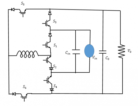
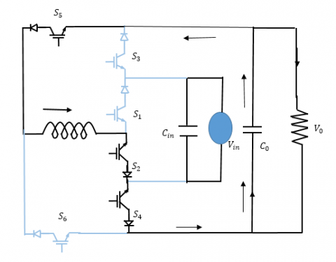
The proposed topology consists of six bidirectional switches, one inductor and two capacitors are used. The bidirectional switches namely, S1 to S6. The proposed topology has been introduced already in literature. In this topology, conventional boost, buck, and buck boost with inverting operation with gain of 1/(1−D), D and −D/(1−D) have been proposed. In this proposed topology, buck and boost modes of operation can be eliminated completely and introduced buck boost operation with non-inverting and voltage gain of D/(1−D) is introduced. The proposed topology is capable to operate variable frequency operation and variable output voltage along with operation of buck-boost capability of input voltage and without shoot through problems of voltage source.
1) Path containing input voltage source and switches S1, S2.
2) Path containing output voltage Voand switches S5, S6.
Path containing input and output voltage and switches S3, S4. However, all the three paths contain two unidirectional switches in opposite (anti-series) direction, and, therefore, the current cannot flow in these close paths. Therefore, shoot through can be avoided in the proposed circuits.
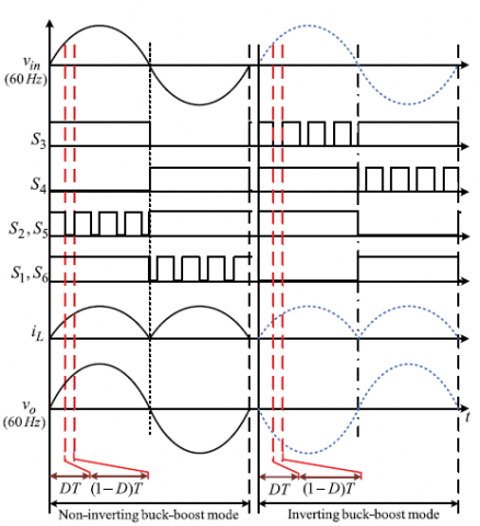
Figure 1. Circuit operation and Switching Strategies for variable frequency operation 60-Hz (Same Frequency, fo= fin) Non-inverting Buck–Boost Operation
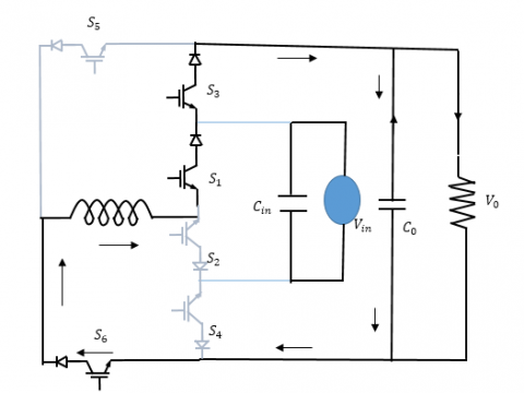
Non inverting buck –boost operation and 60Hz and their waveforms are shown in the Figure 2. From figure 2 it is clearly seen that, switches S1, S3 and S6 are turned ON and switch S4 is completely turned OFF. ON and OFF of high frequency switches S2, S5 are depends on the intervals DT and (1−D)T, respectively. The equivalent circuit of non-inverting buck boost operation of AC to AC converter is shown in the Figure 3. The circuit operation interval is DT and input energy is stored in inductor. Switches S1 and S6 are reverse biased, it is used to preventing from conducting the current. We apply KVL, then
$V _ { L } = V _ { i n }$ (1)
The non-inverting buck-boost mode operation with input voltage is greater than zero with duty duration of DT.
Figure 2. Switching scheme and waveforms for non-inverting and inverting buck–boost operation
Figure 3. Non-inverting buck–boost operation when Vin>0. (a) During DT
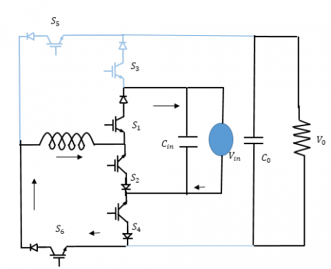
Figure 4. Non-inverting buck–boost operation when Vin>0. During(1 −D)T
The equivalent circuit of non-inverting buck boost operation of AC to AC converter is shown in the Figure 4. The circuit operation interval is (1-D) T and input energy is stored in inductor. Switches S1 and S6 are forward biased, it is used to provide freewheeling path to inductors. S2, S5 are turned OFF during this interval. During this period, energy stored in the inductor is released to load side. We apply KVL, then
$V _ { L } = - V _ { 0 }$ (2)
The non-inverting buck-boost mode operation with input voltage is greater than zero with duty duration of (1-D) T.
Figure 5. Noninverting buck–boost operation when νin<0. (a) During DT and (b) during (1−D)T
During the negative half cycle of supply voltage, switches S2, S4 and S5 are ON and switch S3 is OFF completely. Non inverting buck-boost operation with interval of DT and (1-D)T respectively. The circuit operation for Vin<0 is similar to that for Vin>0, with only difference that now switches S1, S6 act same as S2, S5 (for Vin>0), and vice versa.
Figure 6. Non-inverting buck–boost operation when νin<0. (a) During DT and (b) during (1 − D)T
Now, flux balance (volt–sec) balance condition on inductor L using (1) and (2) gives
$\frac { V _ { 0 } } { V _ { i n } } = \frac { D } { 1 - D }$
From equation, the voltage gain of the proposed converter for this non-inverting buck–boost mode is D/(1−D) having voltage buck operation for D <0.5 and boost operation for D >0.5, with same phase and frequency of output voltage as that of input voltage.
The simulation results of the proposed system are presented in this section. The proposed system is simulated through MATLAB / Simulink and tested. AC–AC converter is cable to operate buck mode and boost mode. In the boost mode duty cycle is more than 0.5. The presented results with duty cycle of 0.8.
3.1. Simulation results: Duty cycle at 0.8 with different frequencies: Boost operation
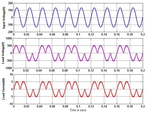
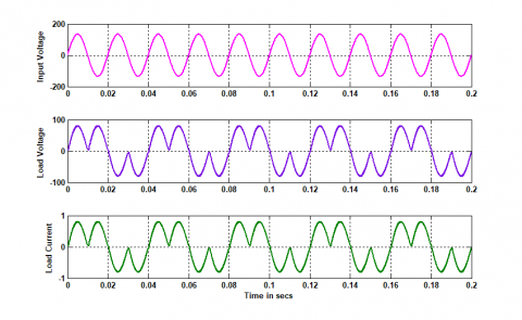
The input voltage, load voltage and load current of the proposed system is shown in the Figure 8. The results is obtained with duty ratio of 0.8 and frequency of 25Hz.
Figure 7. Input voltage, load voltage and load current for 0.8 duty cycle and frequency of 25Hz
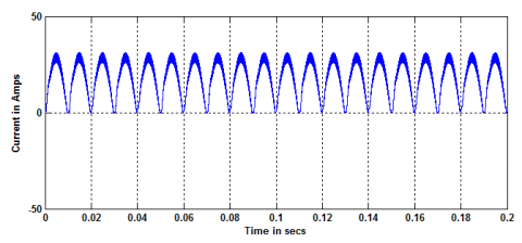
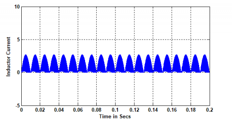
Figure 8. Inductor current for 0.8 duty cycle and frequency of 25Hz
The inductor current of the proposed system is shown in the Figure 8. The results are obtained with duty ratio of 0.8 and frequency of 25Hz.
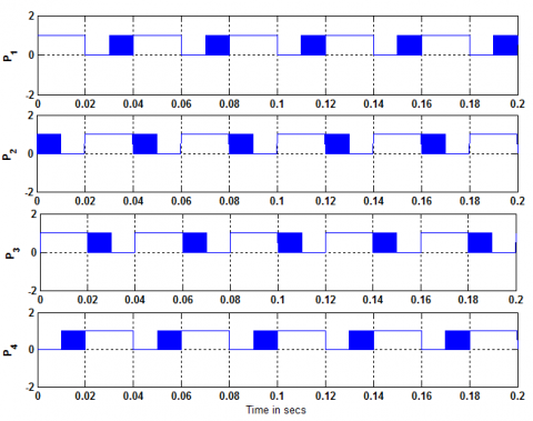
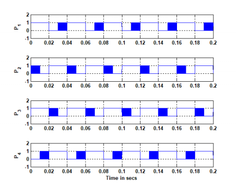
Figure 9. Switching Pulses for 0.8 Duty cycle and Frequency of 25Hz
The switching pulses of the proposed system are shown in the Figure 9. The switching pluses results are obtained with duty ratio of 0.8 and frequency of 25Hz.
3.2. Simulation results: Duty cycle at 0.4 with different frequencies: Buck operation
The boost operation of AC to AC converter is discussed in this section. AC–AC converter is cable to operate buck mode and boost mode. In the buck mode duty cycle is less than 0.5. The presented results with duty cycle of 0.4 and 25Hzfrequency. The Simulink model of AC to AC converter is shown in the Figure 10.
Figure 10. Input voltage, load voltage and load current for 0.4 duty cycle and frequency of 25Hz
The input voltage, load voltage and load current of the proposed system is shown in the Figure 10. The results are obtained with duty ratio of 0.8 and frequency of 25 Hz.
Figure 11. Inductor current for 0.4 duty cycle and frequency of 25 Hz
The inductor current of the proposed system is shown in the Figure 11. The results are obtained with duty ratio of 0.4 and frequency of 25 Hz.
Figure 12. Switching pulses for 0.4 duty cycle and frequency of 25 Hz
The switching pulse of the proposed system is shown in the Figure 12. The switching pluses results are obtained with duty ratio of 0.4 and frequency of 25 Hz.
Design and simulation of buck –boost AC to AC matrix converter with non-inverting and inverting operation and without commutation problems has been presented in this paper. For getting AC-AC conversion, AC voltage regulators are used. This is constructed by thyristors. The control technique may be ether integral or phase control applied. The proposed converter topology uses six unidirectional current flowing and bidirectional voltage blocking switches, implemented by six reverse blocking insulated-gate bipolar transistors (IGBTs) or series MOSFET–diode pairs, two input and output filter capacitors, and one inductor. The proposed work simulated with different input frequency and results are validated with theoretical results. The simulation results have been obtained with different operating frequency and different duty cycle. The performances of the proposed work will be analyzed through MATLAB/Simulink.
Ahmed H. F., Cha H. Y., Aleem Z., Khan A. A., Kim H. G. (2015). A novel buck-boost AC-AC converter with inverting and non-inverting operation and no commutation problem. 9th International Conference on Power Electronics and ECCE Asia (ICPE-ECCE Asia), 1-5 June 2015, Seoul, South Korea. http://dx.doi.org/10.1109/ICPE.2015.7167891
Batarseh I. (2004). Power electronic circuits. Wiley, New York.
Chen B., Gu B., Zhang L., Xahid Z. U., Lai J. S. (2015). A high-efficiency MOSFET transformer less inverter for nonisolatedmicroinverter applications. IEEE Trans. Power Electron., Vol. 30, No. 7, pp. 3610-3622.
dos Santos E. C., Jacobina C. B., Rocha N., da Silva E. R. C. (2011). Sixphase machine drive system with reversible parallel AC-DC-AC converters. IEEE Trans. Ind. Electron., Vol. 58, No. 5, pp. 2049-2053. http://dx.doi.org/10.1109/TIE.2010.2054057
Fang X. P., Qian Z. M., Peng F. Z. (2005). Single-phase Z-source PWM AC–AC converters. IEEE Power Electron. Lett., Vol. 3, No. 4, pp. 121-124. http://doi.org/10.1109/lpel.2005.860453
Hart D. (2011). Power electronics: converters, applications, and design. Wiley, New York.
Kolar J. W., Friedli T., Rodriguez J., Wheeler P. W., Kolar J. W. (2011). Review of three-phase PWM AC-AC converter topologies. IEEE Trans. Ind. Electron., Vol. 58, No. 11, pp. 4088-5006.
Lazzarin T. B., Andersen R. L., Barbi I. (2015). A switched-capacitor three-phase AC-AC converter. IEEE Trans. Ind. Electron., Vol. 62, No. 2, pp. 735-745. http://dx.doi.org/10.1109/TIE.2014.2336625
Lee D. C., Kim Y. S. (2007). Control of single-phase-to-three-phase AC/DC/AC PWM converters for induction motor drives. IEEE Trans. Ind. Electron., Vol. 54, No. 2, pp. 797-804. http://dx.doi.org/10.1109/TIE.2007.891780
Nguyen M. K., Jung Y. G., Lim Y. C. (2010). Single-phase ac-ac converter based on quasi-Z source topology. IEEE Trans. Power Electron., Vol. 25, No. 8, pp. 2200-2209. http://dx.doi.org/10.1109/TPEL.2010.2042618
Rashid M. H. (2010). Power electronics: Circuits, devices and applications. International Economy Edition.