Aneel Kumar Maheshwari* | Mukhtiar Ahmed Mahar | Abdul Sattar Larik | Abdul Hameed Soomro
© 2021 IIETA. This article is published by IIETA and is licensed under the CC BY 4.0 license (http://creativecommons.org/licenses/by/4.0/).
OPEN ACCESS
The paper introduces the cascaded H-Bridge multi-level inverter with single-phase arrangement connected series with full-bridge inverter and CHBMLI configuration integrated with Double level circuit is proposed to reduce the harmonic distortion to get high power quality. In the proposed configuration, a half-bridge inverter has been implemented to increase the output voltage waveform nearly twice as compared with the conventional Cascaded H-Bridge MLI. For high Power quality, the output voltage waveform with the reference of sinusoidal, the phase opposition disposition carrier arrangement has been utilized in PWM for producing gate pulse of switches. The high waveform of output voltage achieved with the less no of switches, less % THD distortion, less conduction and switching losses. The purposed symmetrical model of CHBMLI is successfully verified using MATLAB based on simulation with DLC configuration.
multi-level inverter, cascaded H-Bridge, multicarrier pulse width modulation, Simulink, THD, output voltage
Globally, the production of clean energy is playing an important role in the generation based on renewable energy, however, the electrical parameter like voltage and frequency is not constant due to the nature of generation, which based on renewable energy sources. In the field of industrial application conventional topology of the inverter has been widely used. Conventional inverters are not capable of high power medium voltage application to reducing harmonics contents, it has less efficiency, more switching losses and in long term, constraints have less lifespan. This lead to introduce the growth in multilevel inverter has functioning high-frequency application under the lower loss of switching with high frequency [1].
The Multi-level converter has widely used in static Var compensator because of less switching losses and low harmonic distortion, in power quality, the advantage of Multilevel inverter is good with high capability of voltage [2]. Normally the Multi-level inverter stabilizes the voltage waveform from the sources of DC Voltage via several levels, the Multi-level inverter is useful to reduce the problem of electromagnetic interference and induced motor failure from high frequency switching dv/dt [3]. With the increase in voltage level the reduction harmonics distortion occurs ultimately, the size of the passive filter decrease [4]. Harmonics lead to various problems which affect the performance of the converters [5, 6]. In the Multilevel inverter reducing the DC sources count, the configuration was developed to utilize floating capacitor and bi-directional switches which increases the complexity in the circuit and also increases the switch count, to balancing the capacitor extra circuitry were needed [7]. In Ref. [8], the power cells with cascaded connection proposed less number of switches as comparable with convention CHB, and still, after all that, it requires a more number of switches. A few other topologies are introduced which are attentive to decreasing the power switches [9-11]. The better option seems a multi-level inverter that can synthesize more voltage waveform at the output by utilizing less no of rated switches. With the more number of levels, the voltage wave at output approaches near to sine wave, subsequently improving its THD. Thus, the requirement of filters reduces due to the inverter. Additionally, MLI provides extra advantages like enhanced efficiency, reduced the stress of dv/dt, lesser electromagnetic interference [12-16]. Among all the topologies for high power applications, the multilevel inverter is preferred [17].
In this research paper, a new topology of CHB multi-level inverter, which introduces a combination for reducing switches of Cascaded H-Bridge Multi-Level Inverter with Double level Circuit, is proposed.
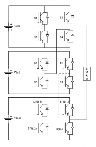
The arrangement of Cascaded H-Bridge Multilevel inverter connected with separate DC sources and series with single-phase full-bridge inverter [18]. The displayed topology of CHBMLI in Figure 1(a). that consists of numbers of bridges or kth full-bridge inverters via a separate DC source. The generated output voltage waveform is obtaining by the summation of every H-Bridge output voltage.
$V_{O=} \sum_{k=1}^{n} V_{H B K}=V_{H B 1}+V_{H B 2}+\cdots+V_{H B n}$ (1)
Here the output voltage of CHBMLI is denoted by Vo and kth H-Bridge output voltage represented by VHBK. The Major Classification of CHBMLI is symmetrical conditions based on DC. In this paper, the configuration of Conventional symmetrical MLI will be discussed. Besides. the proposed CHBMLI with DLC is investigating to increase the quality of power in the form of the voltage waveform and reduce the total harmonics distortion.
(a)
(b)
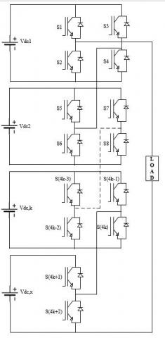
Figure 1. (a). Generalize conventional CHBMLI; (b). Generalize purposed CHBMLI
This Cascaded H-Bridge multilevel inverter plays an important role in reducing the harmonics up to twice as compared with conventional CHBMLI. The configuration of CHBMLI is the combination of the half-bridge inverter with kth bridge inverter in series, which is shown in Figure 1(b). The single half-bridge is integrated with the circuit, which acts as a performance of the double-level circuit. To balance a particular distance from a short circuit, the DLC not only increases the levels of output voltage near to double but also decreases the number of switches and its voltage rating as compared with conventional CHBMLI. In Table 1, by mathematically the generating output voltage level as:
$V_{a}=V_{d c 1}+V_{d c 2}+V_{d c 3}+\cdots+V_{d c k}$ (2)
$L=2 x[(2 x k)+1]-1$ (3)
To avoid the short circuit, the switches of half-bridges are not switching on consecutively [19]. However, a control scheme has been built for purposed CHBMLI to avoid short ckt with turn-on switches of DLC circuit. Table 3 shows the comparison of numbers of different components in conventional and proposed CHBMLI for generating 13-level output voltages.
Table 1. Equation for conventional MLI with propose CHBMLI arrangement
|
Related with |
Conventional MLI |
CHBMLI with DLC |
|
No. of level |
2K + 1 |
2 x (2K+1) – 1 |
|
Switches |
4 K |
4K + 2 |
|
DC Source |
K |
K + 1 |
|
Max. Voltage output |
KVdc |
KVdc |
|
PIV |
4K Vdc |
(4K+1) V dc |
Generally, the configuration of the Symmetrical multilevel inverter is shown in Figure 1(a), there is kth bridge were separated by DC voltage source, the AC voltage waveform produced will the level of (2k + 1). The value of DC source is Equal to 1:1:1:1 so on… or,
$V_{d c z}=V_{d c} \quad \mathrm{z}=1,2,3, \ldots$ so on (4)
Table 2. Switching table for premeditated CHBMLI configuration
|
Mode |
Switch States (ON = 1: OFF = 0) |
Combination |
|||||||||||||
|
S1 |
S2 |
S3 |
S4 |
S5 |
S6 |
S7 |
S8 |
S9 |
S10 |
S11 |
S12 |
S13 |
S14 |
||
|
1 |
0 |
1 |
0 |
1 |
0 |
1 |
0 |
1 |
0 |
1 |
0 |
1 |
1 |
0 |
Vdcx |
|
2 |
1 |
0 |
0 |
1 |
0 |
1 |
0 |
1 |
0 |
1 |
0 |
1 |
0 |
1 |
Vdc1 |
|
3 |
1 |
0 |
0 |
1 |
0 |
1 |
0 |
1 |
0 |
1 |
0 |
1 |
1 |
0 |
Vdc1 + Vdcx |
|
4 |
1 |
0 |
0 |
1 |
1 |
0 |
0 |
1 |
0 |
1 |
0 |
1 |
0 |
1 |
Vdc1 + Vdc2 |
|
5 |
1 |
0 |
0 |
1 |
0 |
1 |
0 |
1 |
0 |
1 |
0 |
1 |
0 |
1 |
Vdc1 + Vdc2 + Vdcx |
|
6 |
1 |
0 |
0 |
1 |
1 |
0 |
0 |
1 |
1 |
0 |
0 |
1 |
0 |
1 |
Vdc1 + Vdc2 + Vdc3 |
|
7 |
0 |
1 |
0 |
1 |
0 |
1 |
1 |
0 |
0 |
1 |
0 |
1 |
1 |
0 |
-Vdc1 + Vdcx |
|
8 |
0 |
1 |
0 |
1 |
0 |
1 |
1 |
0 |
0 |
1 |
0 |
1 |
0 |
1 |
-Vdc1 |
|
9 |
0 |
1 |
1 |
0 |
0 |
1 |
1 |
0 |
0 |
1 |
0 |
1 |
1 |
0 |
-Vdc1 - Vdc2 |
|
10 |
0 |
1 |
1 |
0 |
0 |
1 |
1 |
0 |
0 |
1 |
0 |
1 |
0 |
1 |
-Vdc1 - Vdc2 + Vdcx |
|
11 |
0 |
1 |
0 |
1 |
0 |
1 |
1 |
0 |
1 |
0 |
1 |
0 |
1 |
0 |
-Vdc1 - Vdc2 - Vdc3+ Vdcx |
|
12 |
0 |
1 |
0 |
1 |
0 |
1 |
1 |
0 |
1 |
0 |
1 |
0 |
0 |
1 |
-Vdc1 - Vdc2 - Vdc3 |
Table 3. Comparison between conventional topology with CHBMLI consist on DLC
|
Parameters |
Conventional MLI |
CHBMLI with DLC |
|
No. of Levels |
13 |
13 |
|
No. of Switches |
24 |
14 |
|
No. of DC Sources |
06 |
04 |
|
No of Driver CKT |
24 |
14 |
|
Conduction of switches per voltage level |
12 |
07 |
|
Total Peak Inverse Voltage |
24 Vdc |
13 Vdc |
|
Total Components |
54 |
32 |
That is called a symmetrical configuration. In Figure 1(b). the cascaded H-Bridge MLI connected with DLC, the DC source value of DLC circuit is,
$V_{d c x}=V_{d c 1} /_{2}=V_{d l c}$ (5)
At symmetrical condition operates in CHBMLI, the DC sources value are signified by,
$V_{d c 1}=V_{d c 2}=V_{d c 3}=\cdots=V_{d c k}=V_{d c}$ (6)
Substituting (3) in (2), we obtain,
$V_{0}=k V_{d c}$ (7)
In output voltage waveform, the formula for calculating the levels in respect of DC sources are signified by:
$L_{v}=(2 x k)+1$ (8)
Different modulation techniques are used to generate carrier pulse for switches in inverter concerning switching frequency in CHBMLI, furthermore, the frequency is divided into two categories such as higher switching frequency and fundamental switching frequency [20]. In this paper for achieving high power quality of output voltage waveform, the multicarrier pulse width modulation technique is embraced.
The POD strategy is functioning for the arrangement of carrier pulse, which has sine waveform above the zero lines the carrier signals are out of phase by 180° compare with below the zero line carrier signal, that strategy is more suitable from others to reduce the total % of THD.
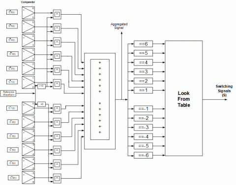
Figure 2 shows the POD-PWM technique with carrier arrangement of POD to generate pulses of 13 level output voltage in the symmetrical configuration of purposed CHBMLI with DLC, with the reference of sine wave zero crossing and the triangular carrier has arranged equally for above and below that generates the Boolean output C1-C12. By using the Boolean output of signal operation based on switching table represent in Table 2, the control scheme has proposed for CHBMLI with DLC would generate output voltage waveform which is given in Figure 3.
Figure 2. POD strategy for CHBMLI with DLC
Figure 3. Control scheme for 13-level inverter
The Simulation modal of symmetrical CHBMLI has been tested with experimental under the condition of CHBMLI with DLC. The configuration of MLI under experimental setup incorporates with 4 DC sources, 14 Switching Devices, Probes of Voltage and current, oscilloscope, PWM technique is POD, Resistive Load is 100 Ω & fundamental switching frequency is 5000 Hz and main frequency is 50 Hz. In cascaded H-Bridge MLI with integrated DLC is valid. The value of the DC voltage source of each bridge is Vdck =30 V and Vdcl = 15V in symmetrical cascaded H-bridge MLI.
5.1 Evolution of power losses
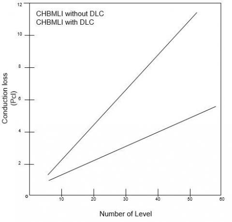
There are two main losses that occur in power electronics switches which are conduction & switching losses. For the system of cooling and estimation of cost scheming in the Multilevel inverter, the power loss calculation is crucial. In the high switching frequency, the losses in switching are considerable & in the low switching frequency, the losses in conduction are more. With the number of levels, the concept of MLI is extended, therefore the relation between no. of switches and no. of level is direct. The power loss will be increased with the increase in the switching count. It is proved that the convention CHB Multilevel inverter has more losses of power compared with the proposed CHMMLI configuration.
The total power loss PL is calculated by the summation of switching losses PSL & Conduction loss PCL.
$P_{L}=P_{S L}+P_{C L}$ (9)
The switching losses can be done by below Eq. (10), and this equation is proved & represented in Refs. [21, 22].
$P_{S L}=f * \frac{1}{6} * V_{S W, K} * I_{K} *\left(t_{O N}+t_{O F F}\right)$ (10)
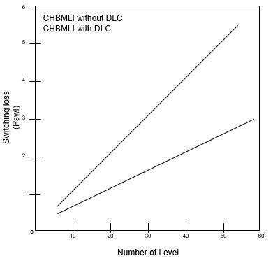
Here, power switching loss represents by PSL, ton represents the turn-on time and toff represents the turn-off time of the kth switch. VSW,K denotes the Kth switch off-state voltage, the fundamental switching frequency is denoted by f, IK represents the current of the switch. Figure 4 represents the PSL (Switching Power loss) for CHBMLI with DLC and without DLC. Due to switches and diode which are connected anti-parallel, the conduction losses occur and the calculation of Conduction losses can be done by subsequent equations.
$P_{C L, K}=\sum_{K=1}^{N}\left(P_{C L . t . k}+P_{C L, d, k}\right)$ (11)
$P_{C L, t, k}=\left[\left(V_{t} * I_{t, a v g}\right)+\left(V_{t} * I_{t r m s}^{2}\right)\right]$ (12)
$P_{C L, d, k}=\left[\left(V_{d} * I_{d, a v g}\right)+\left(V_{d} * I_{d r m s}^{2}\right)\right]$ (13)
Here, Pcl,t,k denotes the conduction loss of switch (kth), Pcl,d,k indicates the loss in conduction of kth anti-parallel diode, on-state voltage of switch is denoted by Vt, the on-state voltage of diode represented by Vd, Vt and Vd represents the collector-emitter on-state resistance of switch and resistance of diode in on-state correspondingly, It,avg and It,rms indicates average current for switch & Root Means square current of the switch, Id,avg, Id,rms indicates the Average diode current & Root Mean Square current of diode respectively. Figure 4 and Figure 5 represent the comparison between Cascaded H-Brige MLI without Double Level Circuit and with DLC and it is verified that the presented CHBMLI has smaller power losses associated with conventional CHBMLI.
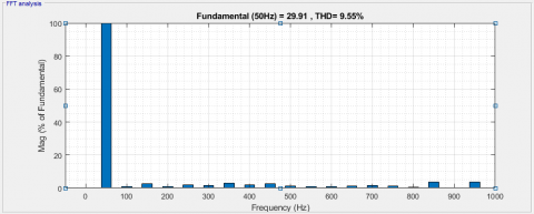
Figure 6 represents the purposed configuration of Cacaded H-Bridge MLI with DLC that produces the output voltage waveform of 13-Level. Figure 7 shows the FFT Analysis of Total Harmonics Distortion upto 9.55%.
Figure 4. Power loss through swiching loss in watts
Figure 5. Power loss through conduction loss in watts
Figure 6. Waveform of output voltage for presented CHBMLI with DLC up to 13-level
Figure 7. The THD of purposed CHBMLI
The paper has discussed the POD-Multicarrier pulse width modulation technique for Cascaded H-Bridge MLI with Double Level Circuit. The POD technique is used for generating the carrier pulse and logical operation has performed for switching in the purposed CHBMLI through symmetrical configuration. The main objective of the research is reducing the number of switching counts and the performance of introducing CHBMLI with DLC is tested. The total harmonics distortion and power losses due to switches is lesser than the Conventional CHBMLI. To verify the results, the Conventional MLI has experienced in the same condition and then compare it. By using Double Level Circuit along with Cascaded H-Bridfge MLI, the output voltage level are twice as related with the Convention CHB-MLI. The presented work is done on MATLAB/Simulink for the consideration of MLI with output voltage waveform and the analysis of THD. The purposed configuration of Cascaded H-Bridge Multilevel inverter with double level circuit gives good power quality and it can be used directly in Permanent Magnet Direct Drive turbine and utility grid that can operate effectively.
To eliminate the problems of power quality, the proposed MLI topology will be tested with FACTS devices.
The sources of renewable energy like solar, wind could be integrated with the proposed topology.
For the operation of grid connection, a suitable current controller could be designed for the proposed topology.
[1] Zulkefle, A.A., Rahman, A.I.A., Zainon, M., Baharudin, Z.A., Zakaria, Z., Farriz, M.B., Shukor, S.A.A, Johan, N.F., Saleh, N., Hanafiah, M.A.R.M. (2018). Modeling and simulation of nine-level cascaded H-Bridge multilevel inverter. Indonesian Journal of Electrical Engineering and Computer Science (IJEECS), 11(2): 696-703. https://doi.org/10.11591/ijeecs.v11.i2.pp696-703
[2] Qureshi, M.R., Mahar, M.A., Larik, A.S. (2020). Harmonic analysis and design of LC filter for a seven-level asymmetric cascaded half bridge multilevel inverter. International Journal of Electrical Engineering & Emerging Technology, 3(2): 52-58.
[3] Lai, J.S., Peng, F.Z. (1996). Multilevel converters-A new breed of power converters. IEEE Transactions on Industry Applications, 32(3): 509-517. https://doi.org/10.1109/28.502161
[4] Tolbert, L.M., Peng, F.Z., Habetler, T.G. (1999). Multilevel converters for large electric drives. IEEE Transactions on Industry Applications, 35(1): 36-44. https://doi.org/10.1109/28.740843
[5] Mahar, M.A., Larik, A.S., Shah, A.A. (2012). Impacts on power factor of AC voltage controllers under nonsinusoidal conditions. Mehran University Research Journal of Engineering and Technology, 31(2): 297-300.
[6] Mahar, M.A., Uqaili, M.A., Larik, A.S. (2011). Harmonic analysis of AC-DC topologies and their impacts on power systems. Mehran University Research Journal of Engineering & Technology, 30(1): 173-178.
[7] Roshankumar, P., Kaarthic, R. S., Gupakumar, K., Leon, J.I., Franquelo, L.G. (2015). A seventeen-level inverter formed by cascading flying capacitor and floating capacitor H-bridge. IEEE Trans. Power Electron, 30(7): 3471-3478. https://doi.org/10.1109/TPEL.2014.2342882
[8] Waltrich, G., Barbi, I. (2009). Three-phase cascaded multilevel inverter using power cells with two inverter legs in series. 2009 IEEE Energy Conversion Congress and Exposition, San Jose, CA, USA, pp. 3085-3092. https://doi.org/10.1109/ECCE.2009.5316460
[9] Alishah, R.S., Nazarpour, D., Hosseini, S.H., Sabahi, M. (2014). Novel topologies for symmetric, asymmetric, and cascade switched-diode multilevel converter with minimum number of power electronic components. IEEE Transactions on Industrial Electronics, 61(10): 5300-5310. https://doi.org/10.1109/TIE.2013.2297300
[10] Ye, Y., Cheng, K.W.E., Liu, J., Ding, K. (2014). A step-up switched-capacitor multilevel inverter with self-voltage balancing. IEEE Transactions on Industrial Electronics, 61(12): 6672-6680. https://doi.org/10.1109/TIE.2014.2314052
[11] Hinago, Y., Koizumi, H. (2011). A switched-capacitor inverter using series/parallel conversion with inductive load. IEEE Transactions on Industrial Electronics, 59(2): 878-887. https://doi.org/10.1109/TIE.2011.2158768
[12] Vijeh, M., Rezanejad, M., Samadaei, E., Bertilsson, K. (2019). A general review of multilevel inverters based on main submodules: Structural point of view. IEEE Transactions on Power Electronics, 34(10): 9479-9502. https://doi.org/10.1109/TPEL.2018.2890649
[13] Aganah, K.A., Luciano, C., Ndoye, M., Murphy, G. (2018). New switched-dual-source multilevel inverter for symmetrical and asymmetrical operation. Energies, 11(4): 984. https://doi.org/10.3390/en11040984
[14] Rodriguez, J., Lai, J.S., Peng, F.Z. (2002). Multilevel inverters: A survey of topologies, controls, and applications. IEEE Transactions on Industrial Electronics, 49(4): 724-738. https://doi.org/10.1109/TIE.2002.801052
[15] Kouro, S., Malinowski, M., Gopakumar, K., et al. (2010). Recent advances and industrial applications of multilevel converters. IEEE Transactions on Industrial Electronics, 57(8): 2553-2580. https://doi.org/10.1109/TIE.2010.2049719
[16] Akagi, H. (2017). Multilevel converters: Fundamental circuits and systems. Proceedings of the IEEE, 105(11): 2048-2065. https://doi.org/10.1109/JPROC.2017.2682105
[17] Pereda, J., Dixon, J. (2012). 23-level inverter for electric vehicles using a single battery pack and series active filters. IEEE Transactions on Vehicular Technology, 61(3): 1043-1051. https://doi.org/10.1109/TVT.2012.2186599
[18] Rodriguez, J., Bernet, S., Steimer, P.K., Lizama, I.E. (2009). A survey on neutral-point-clamped inverters. IEEE transactions on Industrial Electronics, 57(7): 2219-2230. https://doi.org/10.1109/TIE.2009.2032430
[19] Prabaharan, N., Palanisamy, K. (2017). Analysis of cascaded H-bridge multilevel inverter configuration with double level circuit. IET Power Electronics, 10(9): 1023-1033. https://doi.org/10.1049/iet-pel.2016.0506
[20] Kasinathan, P. (2020). Hybrid modulation technique for asymmetrical reduced switch multilevel inverter. Solid State Technology, 63(6): 14656.
[21] Ebrahimi, J., Babaei, E., Gharehpetian, G.B. (2011). A new multilevel converter topology with reduced number of power electronic components. IEEE Transactions on Industrial Electronics, 59(2): 655-667. https://doi.org/10.1109/TIE.2011.2151813
[22] Kangarlu, M.F., Babaei, E. (2012). A generalized cascaded multilevel inverter using series connection of submultilevel inverters. IEEE Transactions on Power Electronics, 28(2): 625-636. https://doi.org/10.1109/TPEL.2012.2203339