Pradeep Kumar
© 2020 IIETA. This article is published by IIETA and is licensed under the CC BY 4.0 license (http://creativecommons.org/licenses/by/4.0/).
OPEN ACCESS
In this paper, nine switches UPQC topology with different control techniques have been depicted and compared their performances to accomplish clear inspection of the best control techniques. As conventional UPQC having twelve switches of six legs enhances the switching losses, circuit complication, costly etc. Hence nine switches UPQC topology is intended to reduce the switching losses, complexity, size and cost. This proposed topology has only three legs with three switches in each leg making total number of nine switches. The three control techniques such as Unit vector template, PQ theory and Synchronous reference frame theory have been employed in the nine switch UPQC topology. The simulation has been carried out separately for each control technique in MATLAB/SIMPOWER environment and results have been verified for higher efficiency of nine switch UPQC topology. The comparative THD of source currents and load voltages under these control techniques have been analysed. The obtained THD values are below 5% as per IEEE-519 standard.
Active and Reactive Power (PQ), Synchronous Reference Frame (SRF), Total Harmonic Distortion (THD), Unified Power Quality Conditioner (UPQC), Unit Vector Template (UVT)
Nowadays, power quality improvements become an important factor for the smooth transfer of power in a distribution system [1-3]. Harmonics in voltage and in current, voltage dip and voltage swell, interruptions, transient over voltage, voltage variations, voltage steps and voltage fluctuations, high reactive power and distortion of voltage and current waveforms are some of the major issues of power quality decrement [3-9]. These power quality problems are caused due to non-linearity behavior of equipment. Nonlinear devices, IT and office equipment, arching devices, load switching, large motor starting, interconnection of power system, lightning strikes and environmental changes are the major sources of power quality issues [3, 5, 8-12]. In industrial scenario, three phase power converters, arching devices and saturable devices are the major source of harmonics in current and voltage. In order to compensate these power quality issues, custom power devices (CPDs) have been employed in distribution lines [2, 3]. Many CPDs have been introduced like DSTATCOM as a shunt compensation, DVR as a series compensation and then UPQC, comprising both shunt and series compensation [13, 14]. The shunt and series inverter of conventional UPQC have 12 switches [15]. The 10-switch based UPQC have been designed and developed in the studies [16-18]. With the increased number of switches, the switching losses and complexity of the circuit will be more which requires complex control technique. Hence 9-s UPQC has been proposed with nine switches for switching loss reduction and to create simplicity of the circuit [19-22].
The practical application of 9-s UPQC topology is in a typical steel manufacturing industry employing induction furnace, arcing devices and saturable devices. More over 9-s UPQC can also be adopted in grid integration of solar PV system. The main work of this paper is to alleviate power quality matters in the distribution network by the proposed 9-s UPQC topology. Different control schemes have been introduced for generation of gate signals for the inverter switches [3, 13, 23-28]. These switches are controlled rectifiers controlled by gate signals which are generated by hysteresis or SPWM generator. In this paper, SRF, UVT and PQ theory have been employed in the nine-switch UPQC and compared their performances in terms of THD (Total harmonic distortion) of source current and load voltage.
2.1 Existing UPQC model
The present UPQC equipped with traditional components; DVR and DSTATCOM which can be combined to form UPQC [13, 14]. In DVR and DSTATCOM, inverter is used, in which six switches are used for series and shunt compensation. The basic structure of UPQC is given in Figure 1 and consists of Shunt compensator, Series compensator, Linear transformer, DC link and Nonlinear load.
Figure 1. Basic UPQC structure
2.2 Proposed UPQC model
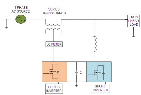
The proposed model consists of both shunt and series compensator but the number of switches get reduced from 12 to 9. The reduction in number of switches not only reduces switching losses but also reduces the complexity of the UPQC system. The new model is termed as 9-S UPQC which utmost will be helpful in getting economical benefits to the distribution companies [19]. The basic structure of proposed UPQC model is given in Figure 2 and can be analyzed by the following points:
a) Dual shunt and series compensator: This compensator consists of total nine switches which can be used as per requirement for the compensation. Upper three switches can be used in series compensation and lower three switches can be used in shunt compensation and the middle switches can be used in both compensations.
b) Linear transformer: This transformer works on the same principle as in traditional UPQC. Similar ratings can be used in both 9-S and normal UPQC.
c) DC link: Similar inductor or capacitor can be used as an energy storing device for maintaining the voltage and current waveform sinusoidal.
Figure 2. 9-S UPQC
Basically control schemes are being used for controlling the switches of inverters used in UPQC [13]. Three different control techniques have been analyzed and compared their performances to examine the best among these.
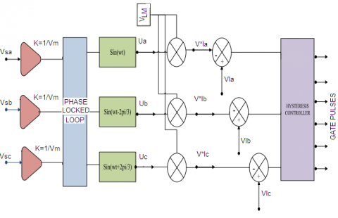
3.1 Unit vector template (UVT)
Unit vector template generates the reference signals of current and voltage for shunt and series inverters respectively. For series inverter, the three phase source voltage is applied to the phase locked loop to achieve the sine angle. From these sine angles, three unit vectors (Ua, Ub and Uc) are obtained as:
$\left[ \begin{matrix} {{U}_{a}} \\ {{U}_{b}} \\ {{U}_{c}} \\ \end{matrix} \right]=\left[ \begin{matrix} 1 & 0 \\ -{}^{1}/{}_{2} & -{}^{\sqrt{3}}/{}_{2} \\ -{}^{1}/{}_{2} & {}^{\sqrt{3}}/{}_{2} \\ \end{matrix} \right]\left[ \begin{matrix} \sin \theta \\ \cos \theta \\ \end{matrix} \right]$ (1)
The three unit vectors are multiplied by the voltage magnitude VLM to get three-phase reference PCC voltages and these reference PCC voltages are compared with the actual PCC voltages.
$\left[ \begin{matrix} V_{la}^{*} \\ V_{lb}^{*} \\ V_{lc}^{*} \\ \end{matrix} \right]={{V}_{LM}} \left[ \begin{matrix} {{U}_{a}} \\ {{U}_{b}} \\ {{U}_{c}} \\ \end{matrix} \right]$ (2)
At last hysteresis controller play important role by converting these compared signals to the gate pulses which is fed to the series inverters for voltage control to the main UPQC circuit. For shunt inverters, voltage error is computed from the comparison of average and the reference value of the dc bus voltage. This error is fed to PI controller (dc voltage controller). The output of PI controller (i.e. reference amplitude (I*Sp) of the supply currents) is multiplied with the three unit vectors (Ua, Ub and Uc) to get three phase reference supply currents.
$\left[ \begin{matrix} I_{Sa}^{*} \\ I_{Sb}^{*} \\ I_{Sc}^{*} \\ \end{matrix} \right]=I_{Sp}^{*} \left[ \begin{matrix} {{U}_{a}} \\ {{U}_{b}} \\ {{U}_{c}} \\ \end{matrix} \right]$ (3)
The computed three-phase supply reference currents are compared with the actual three-phase supply currents and then feed to hysteresis controller to generate the switching signals for the inverter switches. Figure 3 indicates UVT control scheme for series and shunt inverter.
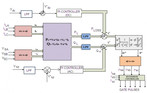
3.2 PQ theory
In this theory Clarke’s and Inverse Clarke’s transformation is used for generating reference signals for gate pulses. In Clarke’s transformation a-b-c rotating reference frame is transformed to α-β-0 static reference frame and vice versa in inverse Clarke’s transformation.
$\left[ \begin{matrix} {{V}_{\alpha }} \\ {{V}_{\beta }} \\ \end{matrix} \right]=\sqrt{\frac{2}{3}} \left[ \begin{matrix} 1 & -{}^{1}/{}_{2} & {}^{1}/{}_{2} \\ 0 & {}^{\sqrt{3}}/{}_{2} & -{}^{\sqrt{3}}/{}_{2} \\ \end{matrix} \right]\left[ \begin{matrix} {{V}_{Sa}} \\ {{V}_{Sb}} \\ {{V}_{Sc}} \\ \end{matrix} \right]$ (4)
$\left[ \begin{matrix} {{I}_{\alpha }} \\ {{I}_{\beta }} \\ \end{matrix} \right]=\sqrt{\frac{2}{3}} \left[ \begin{matrix} 1 & -{}^{1}/{}_{2} & {}^{1}/{}_{2} \\ 0 & {}^{\sqrt{3}}/{}_{2} & -{}^{\sqrt{3}}/{}_{2} \\ \end{matrix} \right]\left[ \begin{matrix} {{I}_{La}} \\ {{I}_{Lb}} \\ {{I}_{Lc}} \\ \end{matrix} \right]$ (5)
Active and reactive power is calculated from the α-β component of voltages and currents.
${{P}_{L}}=({{V}_{\alpha }}*{{I}_{\alpha }})+({{V}_{\beta }}*{{I}_{\beta }}) \\ {{Q}_{L}}=({{V}_{\beta }}*{{I}_{\alpha }})-({{V}_{\alpha }}*{{I}_{\beta }})$ (6)
To achieve DC component of active and reactive power, calculated Active and reactive power is processed through LPF. The loss component of active power Ploss is calculated from compared DC voltage which is obtained from the PI controller. VAR reactive power i.e. Qvr is computed from the compared PCC voltage which is obtained from AC voltage controller. The p* is calculated from Ploss and $\overline{P_{L}}$ and q* is calculated from Qvr and $\overline{Q_{L}}$. The reference current in α-β frame is calculated from the reference value of active and reactive power i.e. p* and q*.
${{P}_{L}}=\overline{{{P}_{L}}}+\overline{\overline{{{P}_{L}}}}, {{Q}_{L}}=\overline{{{Q}_{L}}}+\overline{\overline{{{Q}_{L}}}}$ (7)
${{p}^{*}}=\overline{{{P}_{L}}}+{{P}_{LOSS}}, {{q}^{*}}=\overline{{{Q}_{L}}}-{{Q}_{vr}}$ (8)
From the inverse clarke’s transformation, three phase reference current in a-b-c frame is obtained.
$\left[ \begin{matrix} I_{Sa}^{*} \\ I_{Sb}^{*} \\ I_{Sc}^{*} \\ \end{matrix} \right]=\sqrt{{}^{2}/{}_{3}}\left[ \begin{matrix} 1 & 0 \\ {}^{-1}/{}_{2} & {}^{\sqrt{3}}/{}_{2} \\ {}^{1}/{}_{2} & -{}^{\sqrt{3}}/{}_{2} \\ \end{matrix} \right]{{\left[ \begin{matrix} {{V}_{\alpha }} & {{V}_{\beta }} \\ {{V}_{\beta }} & -{{V}_{\alpha }} \\ \end{matrix} \right]}^{-1}}\left[ \begin{matrix} {{p}^{*}} \\ {{q}^{*}} \\ \end{matrix} \right]$ (9)
This reference three phase current is compared with the actual three phase current and fed to the hysteresis controller to produce gate pulses for thyristors. Figure 4 indicates block diagram representation of PQ Theory for generating gate pulses.
3.3 Synchronous reference frame
In this technique, Phase locked loop (PLL) is synchronized with the PCC voltage and generates phase angle for the Park’s and Inverse Park’s transformation [25, 26]. In Park’s transformation, three phase source current is converted into d- component of source current and then fed to Low pass filter.
$\left[ \begin{matrix} 0 \\ {{I}_{sD}} \\ 0 \\ \end{matrix} \right]=\sqrt{\frac{2}{3}}\left[ \begin{matrix} \frac{1}{\sqrt{2}} & \frac{1}{\sqrt{2}} & \frac{1}{\sqrt{2}} \\ \sin \theta & \sin (\theta -\frac{2\pi }{3}) & \sin (\theta +\frac{2\pi }{3}) \\ \cos \theta & \cos (\theta -\frac{2\pi }{3}) & \cos (\theta +\frac{2\pi }{3}) \\ \end{matrix} \right]\left[ \begin{matrix} {{I}_{Sa}} \\ {{I}_{Sb}} \\ {{I}_{Sc}} \\ \end{matrix} \right]$ (10)
The Low pass filter is used for extraction of DC component of current and voltage i.e. IsDdc and VsDdc. The compared signal of DC capacitance voltage and DC reference voltage is passed through PI controller to generate current loss i.e. Iloss. The current loss i.e. Iloss is to be added with the DC component of IsD to obtain reference current I*D.
$I_{D}^{*}={{I}_{Loss}}+{{I}_{sDdc}}$ (11)
Figure 5. Synchronous reference frame
At last, ID*and VsDdc are transformed to abc component by Inverse Park’s transformation and further sent to hysteresis controller. In hysteresis controller, the reference signals are compared with the corresponding actual signals and generate gate pulses for the thyristors. Figure 5 indicates block diagram of Synchronous reference frame technique.
$\left[ \begin{matrix} I_{Sa}^{*} \\ I_{Sb}^{*} \\ I_{Sc}^{*} \\ \end{matrix} \right]=\sqrt{\frac{2}{3}}{{\left[ \begin{matrix} \frac{1}{\sqrt{2}} & \frac{1}{\sqrt{2}} & \frac{1}{\sqrt{2}} \\ \sin \theta & \sin (\theta -\frac{2\pi }{3}) & \sin (\theta +\frac{2\pi }{3}) \\ \cos \theta & \cos (\theta -\frac{2\pi }{3}) & \cos (\theta +\frac{2\pi }{3}) \\ \end{matrix} \right]}^{-1}}\left[ \begin{matrix} 0 \\ I_{D}^{*} \\ 0 \\ \end{matrix} \right]$ (12)
$\left[ \begin{matrix} 0 \\ {{V}_{sD}} \\ 0 \\ \end{matrix} \right]=\sqrt{\frac{2}{3}}\left[ \begin{matrix} \frac{1}{\sqrt{2}} & \frac{1}{\sqrt{2}} & \frac{1}{\sqrt{2}} \\ \sin \theta & \sin (\theta -\frac{2\pi }{3}) & \sin (\theta +\frac{2\pi }{3}) \\ \cos \theta & \cos (\theta -\frac{2\pi }{3}) & \cos (\theta +\frac{2\pi }{3}) \\ \end{matrix} \right]\left[ \begin{matrix} {{V}_{Sa}} \\ {{V}_{Sb}} \\ {{V}_{Sc}} \\ \end{matrix} \right]$ (13)
$\left[ \begin{matrix} V_{La}^{*} \\ V_{Lb}^{*} \\ V_{Lc}^{*} \\ \end{matrix} \right]=\sqrt{\frac{2}{3}}{{\left[ \begin{matrix} \frac{1}{\sqrt{2}} & \frac{1}{\sqrt{2}} & \frac{1}{\sqrt{2}} \\ \sin \theta & \sin (\theta -\frac{2\pi }{3}) & \sin (\theta +\frac{2\pi }{3}) \\ \cos \theta & \cos (\theta -\frac{2\pi }{3}) & \cos (\theta +\frac{2\pi }{3}) \\ \end{matrix} \right]}^{-1}}\left[ \begin{matrix} 0 \\ {{V}_{sDdc}} \\ 0 \\ \end{matrix} \right]$ (14)
4.1 Series part calculations
4.1.1 Linear transformer
The rating of this transformer can be assigned on the basis of voltage coming from source:
${{V}_{inj}}=X*{{V}_{S}}$ (15)
VA rating of transformer= $3 * V_{i n j} * I_{i n j}$ (sag condition)
4.1.2 Inductors on series side
Secondary side current can be determined by load real power and this current can be helpful to find series inductance.
${{I}_{\sec }}=\frac{{{P}_{L}}}{3*(1+X)*{{V}_{S}}}$ (16)
${{L}_{se}}=\frac{\sqrt{3}}{2}*\frac{M*K*{{V}_{dc}}}{{{f}_{s}}*6*a*{{I}_{\sec }}}$ (17)
4.2 Shunt part calculations
4.2.1 Inductor on shunt side
It can be determined from DC voltage, ripple current and switching frequency.
${{L}_{f}}=\frac{\sqrt{3}*M*{{V}_{dc}}}{12*a*{{f}_{s}}*{{I}_{rc}}}$ (18)
4.2.2 Switch rating of voltage and current
Dynamic conditions can be calculated by following equation;
${{V}_{r}}={{V}_{dc}}+{{V}_{w}}$ (19)
${{I}_{r}}=1.25*({{I}_{rc}}+{{I}_{pk}})$ (20)
4.3 Switching mechanism
There are nine thyristors in 9-S UPQC so in order to work upper six thyristors as series compensator and lower six thyristors as shunt compensators; XOR gate has been used [19]. XOR gate confirms that which thyristors must be working in particular situations. Following scheme has been used for this mechanism:
$G7=\overline{G1.G4}, G8=\overline{G2.G5}, G9=\overline{G3.G6}$
4.4 DC voltage control
For controlling the current of the inverter Vdc means DC voltage across capacitor should be always greater than the line to line voltage (peak) of distribution lines. The DC voltage is selected in such a way that it reduces the ripples as much as possible. It can be calculated as:
${{V}_{DC}}=\frac{2\sqrt{2}*{{V}_{L}}}{\sqrt{3}*m}$ (21)
DC Capacitor value of 9-S UPQC can be calculated from the following equation:
${{C}_{DC}}=\frac{{{K}_{1}}*6*V*I*a*t}{V_{DC}^{2}-V_{DC1}^{2}}$ (22)
The nine-switch UPQC topology with the UVT, PQ and SRF control techniques have been modeled and executed in MATLAB/ simulink environment using sim power tool boxes. The simulation works have been performed by considering 0.8 sec simulation time in ode5 solver.
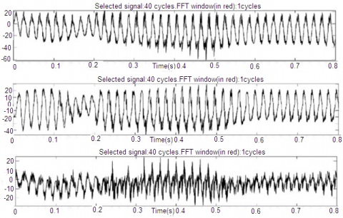
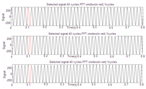
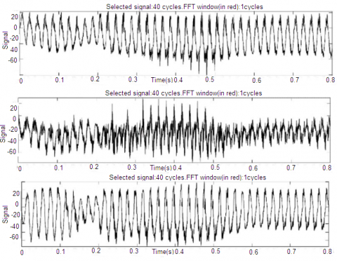
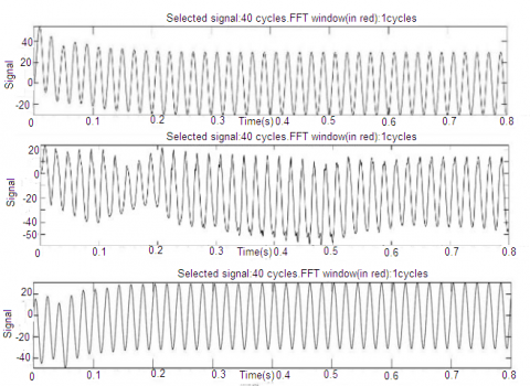
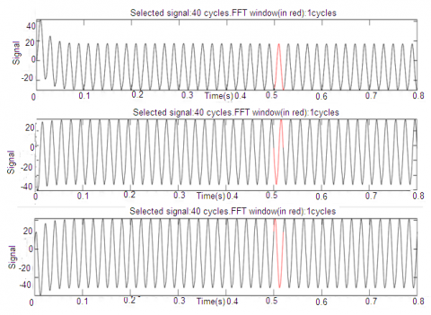
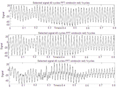
Simulation results in nine-switch UPQC of Figure 6, Figure 7 & Figure 8 show the load voltages of each phase a, b and c under after compensation and before compensation condition for SRF, PQ and UVT theory respectively. The load voltages are compensated by series voltages, injected by DVR circuit of nine-switch UPQC. Previously load voltages are harmonically distorted due to nonlinear loads but after compensation, load voltages become sinusoidal.
(a)
(b)
Figure 6. Three phase load voltages (a) after and (b) before compensation in SRF
(a)
(b)
Figure 7. Three phase load voltages (a) after and (b) before compensation in PQ theory
(a)
(b)
Figure 8. Three phase load voltages (a) after and (b) before compensation in UVT
(a)
(b)
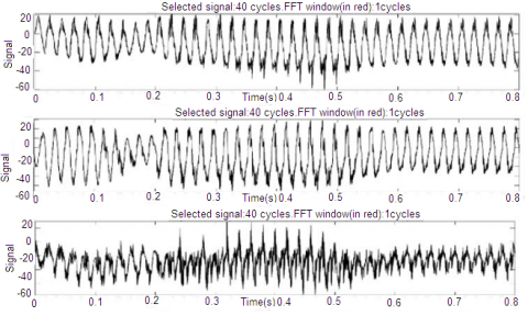
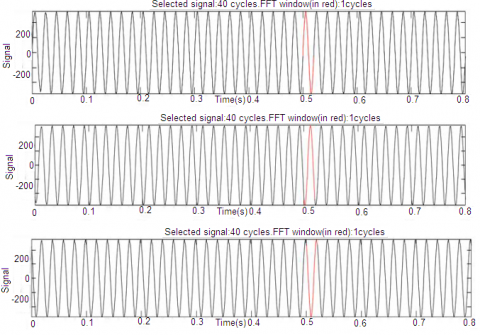
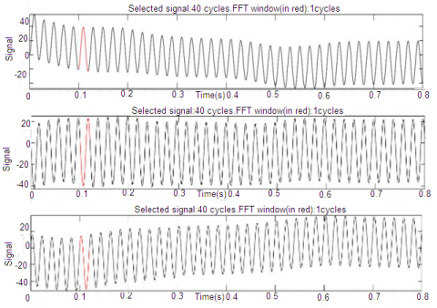
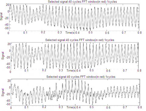
Figure 9. Three phase source currents (a) after and (b) before compensation in SRF
(a)
(b)
Figure 10. Three phase source currents (a) after and (b) before compensation in PQ theory
(a)
(b)
Figure 11. Three phase source currents (a) after and (b) before compensation in UVT
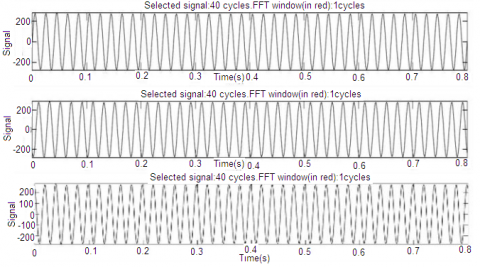
Now the simulation results in nine-switch UPQC topology have been observed by considering source currents parameter. Figure 9, Figure 10 & Figure 11 show the source currents of three phase a, b and c on after compensation and before compensation in SRF, PQ and UVT theory respectively. The source currents are compensated by shunt current injected by DSTATCOM circuit of nine switch UPQC. Previously, source currents are harmonically distorted due to nonlinear loads but after compensation, THD of source current get reduced and become sinusoidal.
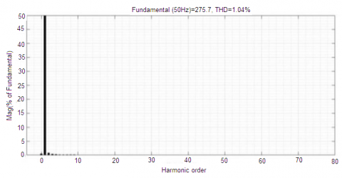
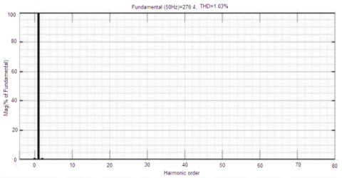
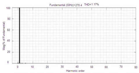
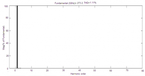
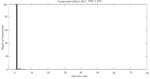
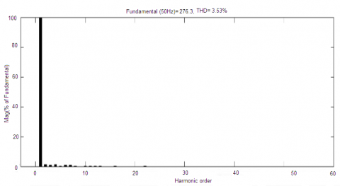
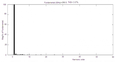
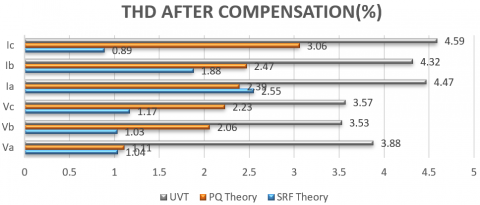
From the simulation results of nine switch UPQC, THD analysis of load voltages have been observed. Figure 12, Figure 13 & Figure 14 depict THD spectrum of load voltages of phase a, b & c after compensation which are 1.04%, 1.03% and 1.17% respectively in SRF control technique, 1.11%, 2.06% and 2.23% respectively in PQ Theory & 3.88%, 3.53% and 3.57% respectively in UVT control technique where the deducted THD values are within the IEEE 519 harmonic Standard limits [29].
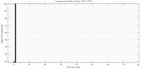
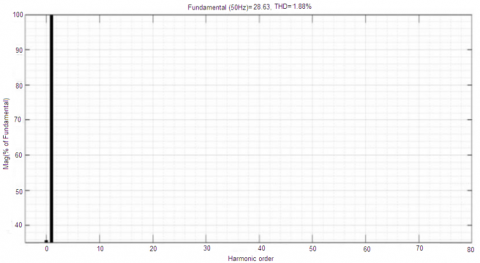
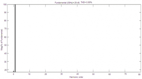
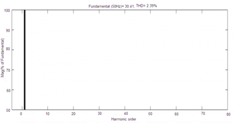
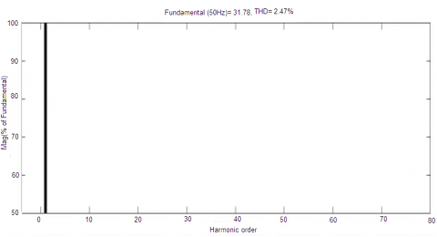
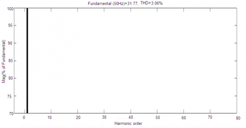
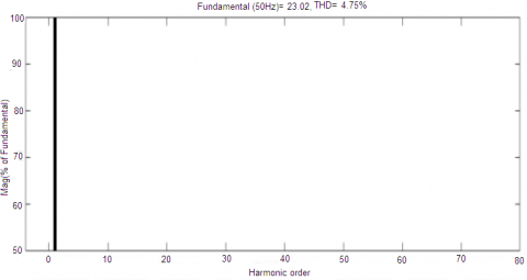
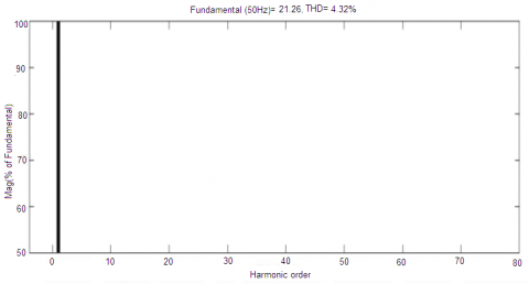
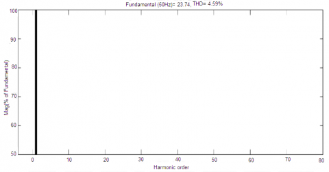
Now the nine switch UPQC results have been explained in terms of source currents THD. Figure 15, Figure 16 & Figure 17 show THD spectrum of Source currents of phase a, b & c for the case of after compensation. In SRF technique, Source currents THD is reduced to 2.55% for phase a, 1.88% for phase b &0.89% for phase c, In PQ Theory, Source currents THD is reduced to 2.39% for phase a, 2.47% for phase b & 3.06% for phase c and In UVT Theory, Source currents THD is reduced to 4.75% for phase a, 4.32% for phase b & 4.59% for phase c. In all control techniques, the deducted THD value of Source currents is less than 5% which successfully fulfills criteria of IEEE 519 standard limits.
Table 1 represents comparative THD analysis of three phase load voltages and source currents for the case of after compensation and before compensation in the nine-switch UPQC topology under SRF, PQ and UVT techniques. From the comparative THD analysis of Table 1, it has been found that the lowest THD value of voltages and currents are achieved by SRF theory. Figure 18 and Figure 19 depict pictorial THD analysis of three phase load voltages and source currents for the case of after compensation and before compensation under SRF, PQ and UVT techniques.
(a) Load Voltage a
(b) Load Voltage b
(c) Load Voltage c
Figure 12. %THD in SRF
(a) Load Voltage a
(b) Load Voltage b
(c) Load Voltage c
Figure 13. %THD in PQ theory
(a) Load Voltage a
(b) Load Voltage b
(c) Load Voltage c
Figure 14. % THD in UVT
(a) Source Current a
(b) Source Current b
(c) Source Current c
Figure 15. %THD in SRF
(a) Source Current a
(b) Source Current b
(c) Source Current c
Figure 16. %THD in PQ theory
(a) Source Current a
(b) Source Current b
(c) Source Current c
Figure 17. % THD in UVT
Figure 18. Pictorial representation of THD (After compensation)
Figure 19. Pictorial representation of THD (Before compensation)
Table 1. THD analysis of load voltage and source current
|
THD AFTER COMPENSATION (%) |
||||
|
|
|
SRF Theory |
PQ Theory |
UVT |
|
Three Phase Load voltages |
Va |
1.04 |
1.11 |
3.88 |
|
Vb |
1.03 |
2.06 |
3.53 |
|
|
Vc |
1.17 |
2.23 |
3.57 |
|
|
Three Phase Source currents |
Ia |
2.55 |
2.39 |
4.75 |
|
Ib |
1.88 |
2.47 |
4.32 |
|
|
Ic |
0.89 |
3.06 |
4.59 |
|
|
THD BEFORE COMPENSATION (%) |
||||
|
|
|
SRF Theory |
PQ Theory |
UVT |
|
Three Phase Load voltages |
Va |
16.72 |
39.80 |
39.80 |
|
Vb |
26.89 |
42.29 |
42.29 |
|
|
Vc |
20.37 |
80.74 |
86.23 |
|
|
Three Phase Source currents |
Ia |
18.29 |
25.54 |
25.54 |
|
Ib |
24.85 |
23.42 |
23.42 |
|
|
Ic |
17.31 |
85.14 |
91.50 |
|
Now a days, there are many custom power devices such as DSTATCOM, DVR used in power distribution system and UPQC is most efficient among all due to its dual scheme simultaneous compensation in the source current and the load voltage. UPQC also have different topologies having different number of switches. This paper presents the comparative analysis of SRF, PQ and UVT based nine-switch UPQC topology. From the comparative analysis, it has been found that SRF based nine-switch UPQC topology is much efficient in reducing THD in load voltages and source currents to large extent as compared to PQ and UVT control techniques. Moreover, due to decrease in switches from 12 to 9, nine-switch UPQC topology have less switching losses which reduce upto 33%. It has been also concluded that the THD in load voltages and source currents of all the three control schemes satisfy the IEEE 519 harmonic standards limits.
|
CPD |
Custom Power Device |
|
DC |
Direct Current |
|
DSTATCOM |
Distribution STATCOM |
|
DVR |
Dynamic Voltage Restorer |
|
IEEE |
Institute of Electrical and Electronics Engineers |
|
PCC |
Point of Common Coupling |
|
PI |
Proportional Integral |
|
PLL |
Phase-Locked Loop |
|
PQ |
Power Quality |
|
SRF |
Synchronous Reference Frame |
|
THD |
Total Harmonic distortion |
|
UPQC |
Unified Power Quality Conditioner |
|
VSI |
Voltage Source Inverter |
|
VA |
Volt Ampere |
Table. Parameters used in simulations and mathematical modeling
|
Elements |
Parameters |
Values |
|
AC Source |
Voltage Va, Vb, Vc |
110 V |
|
Frequency f |
50 Hz |
|
|
Resistance |
0.01 Ώ |
|
|
Inductance |
10 mH |
|
|
Linear transformer |
Nominal Power |
2 KVA |
|
Frequency |
5 Hz |
|
|
Series Line Impedance |
Resistance (Rse) |
1 Ώ |
|
Inductance (Lse) |
5 mH |
|
|
Shunt line Impedance |
Resistance (Rsh) |
1 Ώ |
|
Inductance (Lsh) |
3 mH |
|
|
DC voltage Capacitance |
Capacitance (Cdc) |
5000μF |
|
Modulation Index |
m |
1 |
|
Turns Ratio |
k |
3 |
|
Voltage Variation |
X |
30% |
|
Overloading Factor |
a |
1.2 |
|
DC dynamic voltage |
Vw |
10% |
|
Ripple current |
Irc |
15-20% |
|
Non Linear loads |
Three phase diode rectifier |
- |
|
Nominal load Rn |
10 Ώ |
|
|
Nominal load Ln |
5mH |
[1] Moreno-Munoz, A. (2007). Power Quality: Mitigation Technologies in a Distributed Environment. Springer-Verlag, Germany.
[2] Ghosh, A., Ledwich, G. (2002). Power quality Enhancement Using Custom Power Devices. Kluwer Academic Publishers, London.
[3] Singh, B., Chandra, A., Al-Haddad, K. (2014). Power Quality: Problems and Mitigation Techniques. John Wiley & Sons.
[4] Fuchs, E., Masoum, M.A. (2011). Power Quality in Power Systems and Electrical Machines. Academic Press.
[5] Bollen, M.H. (2000). Understanding Power Quality Problems. In Voltage Sags and Interruptions. IEEE Press. http://doi.org/10.1109/9780470546840
[6] Tabatabaei, N.M., Aghbolaghi, A.J., Bizon, N., Blaabjerg, F. (2017). Reactive power control in AC power systems. Switzerland: Springer. http://doi.org/10.1007/978-3-319-51118-4
[7] Arrilaga, J., Wattson, N.R., Chen, S. (2000). Power system quality assessment. Power System Quality Assessment, p. 312. http://doi.org/10.1002/9780470682111.ch4
[8] Mikkili, S., Panda, A.K. (2018). Power Quality Issues: Current Harmonics. CRC Press.
[9] Dugan, R.C., Mc Granaghan, M.F., Santoso, S., Beaty, H.W. (2004). Electric Power Systems Quality. 2nd ed., McGraw Hill, USA.
[10] Kashif, M., Hossain, M.J., Zhuo, F., Gautam, S. (2018). Design and implementation of a three-level active power filter for harmonic and reactive power compensation. Electric Power Systems Research, 165: 144-156. https://doi.org/10.1016/j.epsr.2018.09.011
[11] Unnikrishnan, A.K., Chandira, S.E., Subhash, J.T.G., Manju, A.S., Joseph, A. (2015). Shunt hybrid active power filter for harmonic mitigation: A practical design approach. Sadhana, 40(4): 1257-1272. https://doi.org/10.1007/s12046-015-0370-x
[12] Pinto, J.G., Pregitzer, R., Monteiro, L.F., Couto, C., Afonso, J.L. (2007). A combined series active filter and passive filters for harmonics, unbalances and flicker compensation. In 2007 International Conference on Power Engineering, Energy and Electrical Drives, pp. 54-59. https://doi.org/10.1109/POWERENG.2007.4380200
[13] Gu, J.J., Xu, D.G., Liu, H.K., Gong, M.Z. (2002). Unified Power Quality Conditioner (UPQC): The principle, control and application. Power Conversion Conference, pp. 80-85. http://doi.org/10.1109/PCC.2002.998518
[14] Khadkikar, V. (2012). Enhancing electric power quality using UPQC: A comprehensive overview. IEEE Transactions on Power Electronics, 27(5): 2284-2297. http://doi.org/10.1109/TPEL.2011.2172001
[15] Modesto, R.A., da Silva, S.A.O., de Oliveira, A.A., Bacon, V.D. (2015). A versatile unified power quality conditioner applied to three-phase four-wire distribution systems using a dual control strategy. IEEE Transactions on Power Electronics, 31(8): 5503-5514. http://doi.org/10.1109/TPEL.2015.2487867
[16] Thentral, T.T., Jegatheesan, R., Vijayakumar, K. (2019). Unified power quality conditioner with reduced switch topology for distributed networks. Wireless Networks, 1-15. https://doi.org/10.1007/s11276-019-02189-y
[17] Rauf, A.M., Sant, A.V., Khadkikar, V., Zeineldin, H.H. (2015). A novel ten-switch topology for unified power quality conditioner. IEEE Transactions on Power Electronics, 31(10): 6937-6946. https://doi.org/10.1109/TPEL.2015.2509510
[18] Jones, M., Vukosavic, S.N., Dujic, D., Levi, E., Wright, P. (2008). Ten switch inverter PWM technique for reduced switch count two-motor constant power applications. IET Proc. Electric Power Applicat., 2(5): 275-287. https://doi.org/10.1049/iet-epa:20070497
[19] Zhang, L., Loh, P.C., Gao, F. (2011). An integrated nine-switch power conditioner for power quality enhancement and voltage sag mitigation. IEEE Transactions on Power Electronics, 27(3): 1177-1190. https://doi.org/10.1109/TPEL.2011.2115256
[20] Bahman, A.S., Loh, P.C., Qin, Z., Blaabjerg, F. (2014). Loss comparison of different nine-switch and twelve-switch energy conversion systems. In 2014 IEEE Applied Power Electronics Conference and Exposition-APEC 2014, pp. 309-314. https://doi.org/10.1109/APEC.2014.6803326
[21] Loh, P.C., Bahman, A.S., Qin, Z., Blaabjerg, F. (2013). Evaluation of switch currents in nine-switch energy conversion systems. In IECON 2013-39th Annual Conference of the IEEE Industrial Electronics Society, pp. 755-760. https://doi.org/10.1109/IECON.2013.6699229
[22] Oka, K., Nozawa, Y., Omata, R. (2007). Characteristic comparison between five-leg inverter and nine-switch inverter. In Proc. Power Convers. Conf., Nagoya, Japan, pp. 279-283. https://doi.org/10.1109/PCCON.2007.372981
[23] Prathyusha, D., Venkatesh, P. (2015). UVTG control strategy for three phase four wire UPQC to improve power quality. Int. Electr. Eng., 6(9): 1988-1993.
[24] Premalatha, S., Dash, S.S., Babu, P.C. (2013). Power quality improvement features for a distributed generation system using shunt active power filter. Procedia Engineering, 64: 265-274. https://doi.org/10.1016/j.proeng.2013.09.098
[25] Kota, V.R., Vinnakoti, S. (2018). Performance evaluation of UPQC under nonlinear unbalanced load conditions using synchronous reference frame based control. Journal of The Institution of Engineers (India): Series B, 99(1): 37-48. https://doi.org/10.1007/s40031-017-0305-5
[26] Kumar, P., Kumar, N., Akella, A.K. (2014). A simulation based case study for control of DSTATCOM. ISA transactions, 53(3): 767-775. https://doi.org/10.1016/j.isatra.2013.11.008
[27] Khadkikar, V., Chandra, A. (2010). Three-phase and single-phase PQ theories applied to three-phase shunt active power filter under different operating conditions: A comparative evaluation. International Journal of Emerging Electric Power Systems, 11(2): 1-8. https://doi.org/10.2202/1553-779X.2308
[28] Devassy, S., Singh, B. (2017). Modified PQ-theory-based control of solar-PV-integrated UPQC-S. IEEE Transactions on Industry Applications, 53(5): 5031-5040. https://doi.org/10.1109/TIA.2017.2714138
[29] Duffey, C.K., Stratford, R.P. (1989). Update of harmonic standard IEEE-519: IEEE recommended practices and requirements for harmonic control in electric power systems. IEEE Transactions on Industry Applications, 25(6): 1025-1034. https://doi.org/10.1109/28.44238