Banumathi Jayaraj*![]() | Karthy Gopalan
| Karthy Gopalan![]()
© 2025 The authors. This article is published by IIETA and is licensed under the CC BY 4.0 license (http://creativecommons.org/licenses/by/4.0/).
OPEN ACCESS
Digital signal processors (DSPs) require good CPU core integration to perform complex processes such as convolution, transformation, and filtering, which rely primarily on multiplication and accumulation. The multiply-accumulate (MAC) unit is crucial for DSP algorithms that require high performance. This paper proposes a high-speed and low-power MAC unit that employs a Pipelined Urdhva-Tiryagbhyam Vedic Multiplier (PUVM) technique based on the Ladner-Fischer adder (LFA). The design is proven using Kintex, Artix, and Virtex FPGAs in Xilinx Vivado 2022.2 and ASIC 45 nm technology, which improves performance. At different bit widths, the suggested PUVM-LFA achieves latency reductions of 43%, 61.55%, 73.04%, and 79.49%. The MAC-PUVM-LFA design achieves a 66.04% reduction in latency and a 19.49% reduction in FPGA area. It boosts power by 71.80% and 74.15%, delays by 87.21% and 87.21%, APP by 18.37% and 39.07%, ADP by 62.98% and 69.86%, and PDP by 96.39% and 96.99% in ASIC. The results show that the suggested technique beats previous solutions in the literature, despite its dependability and low cost.
Ladner-Fischer adder, UVM, multiply-accumulate unit, digital signal processors, pipelining, field programmable gate array
The MAC unit plays a vital role in DSP systems, significantly impacting processor performance in applications like FIR filters, FFT, and convolution that rely on complex arithmetic operations. Reducing latency by MAC units leads to improved performance [1]. VMs have been used to design an efficient MAC unit, and area and delay characteristics have been compared [2]. A successful development of a high-speed MAC unit has been made [3]. A typical Brent-Kung adder-based (BKA) unit is almost five times slower than the suggested MAC unit [4]. There are two suggested 32-bit MAC architectures: one with a Carry Save Adder, VM, and a Ripple Carry Adder (RCA), and an Array Multiplier (AM) [5]. There have been two proposed 32-bit MAC architectures, one using AM and the other using VM [6]. To maximize the computing of neural networks, MAC units are compared for energy, throughput, and area [7].
Convolutional neural networks have been suggested to use a fully customized 8-bit MAC architecture in place of embedded memories and DSP blocks [8]. A feasible choice for high-performance applications, VMs are distinguished by their effective architecture, which is typified by low power consumption and decreased delay. This is demonstrated in Table 1's comparisons of implementation characteristics, area, latency, power consumption, and complexity with various multiplier architectures, such as the Array, Wallace, Booth, and Dadda multipliers. Many creative multiplier designs have been created: A Booth-Vedic hybrid architecture has been developed to improve efficiency in both area and speed [9]. Using inexact adders and clock-gating, approximation multipliers have been shown to improve speed and minimize power usage [10]. Using a hybrid compressor, a new multiplier has been presented [11]. Using the Anurupyena sub-sutra, multiplication operations have been carried out using the Vedic technique [12].
The Vedic method based on the UT Sutra has been examined for its use in multiplication [13]. To maximize area and power, an effective 4:2 compressor design was employed [14]. By integrating UT Sutra with Booth and Vedic methods, efficient multiplication of signed digits has been made possible [15]. Cadence Virtuoso and 45nm technology were utilized to design a 4-bit VM for enhanced speed [16]. Utilizing the UT technique, a modular VM architecture was created [17]. A square architecture with a low area consumption was created [18]. Using 4 × 4 blocks, an 8 × 8 VM was built on a Kintex-7 FPGA board [19]. They introduced a parallel signed multiplier without sign extension [20]. For cryptography applications, a high-speed multiplier unit was put into place [21]. UT Sutra was used to design a 32-bit VM [22]. Redundant data detectors and compressors were used in the architecture of reconfigurable VMs [23]. Single-precision floating-point multipliers were implemented using compressor designs [24]. For high-speed Booth multipliers, new compressor structures were employed [25].
The UT Sutra from Vedic Mathematics was used to develop high-speed multipliers, which were then implemented using LFA. This work enhanced latency, area, and energy efficiency, particularly for larger bit sizes.
Table 1. Comparison of multipliers
|
Parameters |
Array Multiplier |
Shift and Add |
Wallace Tree Multiplier |
Booth Multiplier |
Vedic Multiplier (VM) |
|
Area |
High |
Less |
Medium |
Medium |
Medium |
|
Power Consumption |
High |
Less |
Medium |
Medium |
Medium |
|
Delay |
Medium |
Large |
Smallest |
Less |
Smallest |
|
Complexity |
Simple |
Simple |
Complex |
Complex |
Simple |
|
Implementation |
Easy |
Easy |
Difficult |
Medium |
Medium |
Among the contributions made to this study were:
(1) In partial product addition, pipelining is employed to reduce VM latency via LFA.
(2) Efficient MAC units were developed using pipelined UVMs and LFA.
(3) VMs are used to process items that need to multiply quickly and efficiently.
(4) The LFA produced less delay and lower power of addition.
The suggested MAC unit improved delay and power by using low-power and high-speed PUVM-LFA.
The manuscript is structured as follows: Part 2 explains Parallel Prefix Adders (PPA), Part 3 covers VM, Part 4 introduces the Proposed PUVM, Part 5 discusses the Proposed MAC unit and results in Part 6, and Part 7 concludes the manuscript.
Adders are essential in multipliers for summing partial products. PPAs efficiently add binary integers in parallel, outperforming sequential adders. PPAs utilize a tree structure to compute carries, reducing propagation latency rapidly. The PPA consists of three fundamental stages.
(a) Pre-processing stage: At this stage, intermediate signals must be produced for each bit position. Each bit in the binary numbers being added produces a "generate" and "propagate" signal.
Generate (g): This bit generates a carry (when the sum exceeds one).
$\text {G}_\text {i}=\text {a}_\text {i} \cdot \text {b}_\text {i}$ (1)
Propagate (p): If a carry occurs, this bit propagates it.
$\mathrm{P}_{\mathrm{i}}=\mathrm{a}_{\mathrm{i}} \oplus \mathrm{b}_{\mathrm{i}}$ (2)
These signals are crucial for efficient carry computation in PPAs.
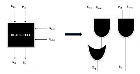
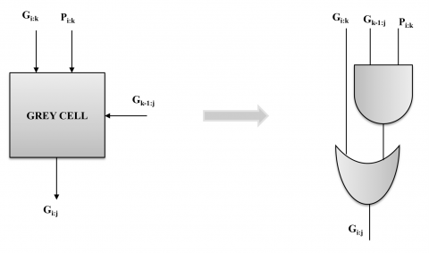
(b) Carry generation stage: Carry-lookahead logic is implemented using Black Cells and Grey Cells to generate carry signals for each bit location, as shown in Figure 1. The carry signals are computed through concurrent algorithms in a tree-like structure, merging pairs of bits in consecutive steps based on produce and propagate signals.
(a)
(b)
Figure 1. (a) Black cell (b) Grey cell
(c) Sum generation stage: This step consists of creating sum bits for each bit location. The total for each bit is then determined by XORing the appropriate propagate value with the carry.
$\mathrm{S}_{\mathrm{i}}=\mathrm{P}_{\mathrm{i}} \oplus \mathrm{c}_{\mathrm{i}}$ (3)
$\mathrm{C}_{\mathrm{i}+1}=\mathrm{G}_{\mathrm{i}}+\mathrm{P}_{\mathrm{i}} \mathrm{c}_{\mathrm{i}}$ (4)
PPAs enable logarithmic time addition, significantly enhancing speed, particularly for large bit widths, and are widely used in applications like digital signal processing, encryption, and microprocessors. Common PPA types include Kogge-Stone Adder (KSA) and BKA, with LFA architecture offering fast addition while reducing power consumption. The choice of adder depends on the application's specific needs, with PPAs greatly influencing digital system design performance [26, 27]. Research has evaluated and compared PPA performance in terms of power dissipation, delay, and area consumption [28, 29]. While KSA offers the least delay, it uses more resources, and BKA optimizes the area at the cost of delay. LFA provides a balance, making it suitable for both delay and area optimization [29]. Various studies have explored high-speed adders for arithmetic applications [30, 31], and efficient multiplier designs, like the Synchronous Pipelined Array Multiplier, have been developed for specific applications [32].
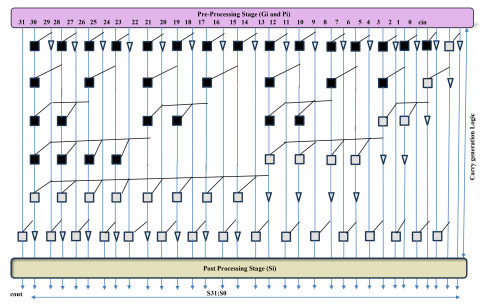
2.1 LFA architecture
The LFA is a high-speed parallel prefix adder designed by Ladner and Fischer in 1980, as shown in Figure 2. The LFA uses a recursive binary addition approach with a tree-like structure that enables efficient computation of carry signals, making it one of the fastest adders due to its minimal logic depth. LFA offers a balance between area and latency, allowing for a trade-off between the two. This design makes LFA suitable for applications requiring both speed and efficiency, positioning it as a balanced option between other fast adders like KSA and area-efficient options like Brent-Kung Adder BKA.
Figure 2. 32-bit Ladner Fischer Adder (LFA) architecture
VM's efficient algorithm and architecture enable faster speeds, reduced latency, and lower power consumption. Vedic mathematics accelerates operations by minimizing complicated computations, making it ideal for applications such as MAC units. It's many strategies that outperform conventional designs. VMs, which are derived from ancient Indian Vedic mathematics, multiply using 16 sutras. Notably, the Nikhilam, Anurupye, and UT sutras present a variety of approaches. The UT Sutra provides various benefits, including faster performance, a smaller footprint, reduced power consumption, a simpler architecture, and more scalability.
3.1 Urdhva-Tiryagbhyam Vedic Multiplier
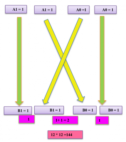
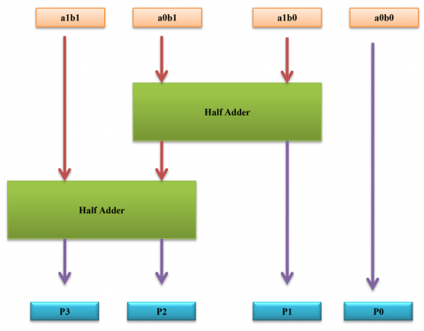
The Urdhva Tiryagbhyam (UT) method utilizes a "vertically and crosswise" technique for multiplication. This approach can be applied to construct larger n*n multipliers by scaling up from the fundamental 2*2 multiplication block, as shown in Figure 3(a), enabling efficient multiplication operations for various bit sizes.
A 2*2 multiplier unit, as shown in Figure 3(b), consists of four AND gates generating partial products and two half-adders for addition. It multiplies two 2-bit numbers (a1a0 and b1b0), where the LSB is obtained by multiplying vertically, the second bit by adding the cross product and carry, and the third and fourth bits are generated from the sum and carry of the partial products of the most significant bits. This unit serves as a fundamental building block for larger multiplier implementations.
(a)
(b)
Figure 3. (a) 2 × 2 demonstration of vedic multiplication (b) 2-bit vedic multiplier
One technique for speeding up and improving the efficiency of digital circuits in VLSI design is pipelining. Pipelining enables more rapid signal processing and greater throughput by breaking computations into simultaneous phases. Pipelining is suitable for high-speed applications in which performance is more important than space limitations, although more space is needed for registers and control logic.
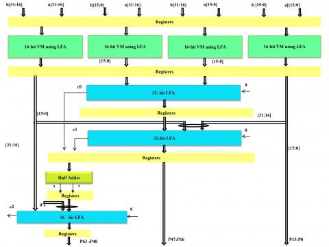
The proposed PUVM-LFA architecture shows a 32 × 32 VM pipeline structure as indicated in Figure 4. The structure comprises two 32-bit LFAs, a half-adder, one 16-bit LFA, and four 16 × 16 VMs with LFA. The structure balances combinational logic paths and achieves maximum efficiency using pipelining with well-placed registers. The registers are wisely placed in between important stages, including:
(1) Input and Output: To enable smooth data transfer between stages, input and output data are kept in registers.
(2) Multiplier and Adder Unit: To enable fast and efficient computation, the intermediate results are kept in registers.
(3) Adders at Various Levels: Partial sums are kept in registers, thus enabling complex arithmetic operations to be performed quickly.
It possesses several noteworthy advantages over current designs, including:
Increased Speed: The design is suitable for applications where speed is high because of its significant delay optimization.
Power Efficiency: The design reduces power consumption by limiting the application of logic gates and minimizing switching operations.
Designing efficient DSP systems involves knowing the trade-offs and physical significance of delay, power, and area. Through a compromise between these factors, the proposed PUVM-LFA architecture enhances delay performance at less power usage. The delay is defined as the time taken by a signal to pass through a digital circuit. System performance is increased, and data processing becomes faster by reducing the delay. In the case of DSP systems, power consumption is an important factor, particularly for battery-powered systems or high-performance computing systems. Battery life, heat dissipation, and system reliability improve if power consumption is reduced.
The improved delay performance and reduced power consumption of the proposed PUVM-LFA architecture render it a good candidate for various real-world applications, including 5G communication and IoT edge devices. System-level design, application-specific optimization, and implementation/test can be explored in future studies to optimize its benefits and establish its functionality in real-world environments.
And it can be applied for data analysis, artificial intelligence, cryptography, and scientific simulations on high-performance computing for bit widths of 128 bits or wider. Rapid insights, secure data transport, and accelerated AI workloads are enabled by its scalability, low power usage, and high-speed performance, which are suitable for applications requiring efficient arithmetic operations.
Figure 4. 32-bit proposed PUVM-LFA
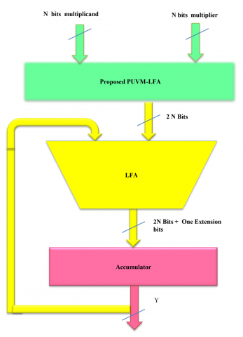
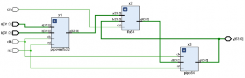
In real-time and DSP applications, the MAC unit is a critical component that facilitates performing complicated mathematical operations efficiently. It is important because it can perform multiply-accumulate operations, which are crucial to DSP algorithms such as Fourier transforms, filtering, and convolution. The performance of the MAC unit has a direct influence on the overall efficiency and accuracy of these applications. The proposed MAC unit architecture, as indicated in Figure 5, is intended to provide performance optimization, power saving, and area usage efficiency. It is made up of a multiplier stage that uses the PUVM-LFA, an adder stage that uses the LFA, and a 2N-bit accumulator. For their capability to be used to maximize DSP and real-time applications, such as embedded systems, telecommunication, and image and audio processing, two MAC unit implementations, namely MAC-UVM-LFA and MAC-PUVM-LFA, are studied in this research.
Figure 5. Architecture of proposed MAC-PUVM-LFA
6.1 FPGA implementation
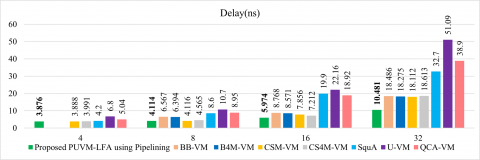
The complete framework is developed using Xilinx Vivado software, which operates on Kintex, Artix, and Virtex processors. We implement the suggested PUVM-LFA in the Kintex 7 series and simulate the outcomes utilizing the XC7K325-2FFG900 device specification. It is known that the suggested PUVM-LFA has a lower latency than alternative multipliers. Table 2 compares the proposed PUVM-LFA's delays to those of other current VMs, and Figure 6(a) depicts the comparison chart. The “–” indicates the values are not mentioned in the references.
It shows a comparison of combinational delay, in which the suggested PUVM-LFA is enhanced. -, -, 0.31%, 2.88%, 7.71%, 43%, and 23.10% for 4-bit width; 37.35%, 35.66%, 0.05%, 0.07%, 52.16%, 61.55%, and 54.03% for 8-bit width; 31.87%, 30.30%, 23.96%, 17.17%, 69.98%, 73.04%, and 68.42% for 16-bit width; and 43.30%, 42.65%, 42.13%, 43.69%, 67.95%, 79.49%, and 73.06% for 32-bit width as compared to BB-VM, CS4M-VM, SquA, U-VM, and QCA-VM, respectively.
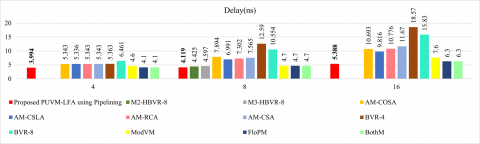
The designed PUVMLFA has been evaluated on the Artix-7 XC7A100T-CSG324 device to simulate and validate its performance. Table 3 compares the proposed PUVM-LFA's delays to those of other current VMs, and Figure 6(b) depicts the comparison chart. The comparison demonstrates how the proposed PUVM-LFA reduces combinational latency. 25.25%, 25.15%, 25.25%, 25.25%, -, -, 25.53%, 38.18%, 13.17%, 2.59%, and 2.59% for four 4-bit widths; 47.82%, 41.08%, 43.59%, 45.55%, 6.92%, 10.40%, 67.28%, 60.97%, 12.36%, 12.36%, and 12.36% for 8-bit widths; and 49.61%, 45.11%, 50%, 53.83%, -, -, 70.99%, 65.96%, 29.11%, 14.48%, and 14.48% for 16-bit widths as compared to M2-HBVR-8, M3-HBVR-8, AM-COSA, AMCS-LA, AM-RCA, AM-CSA, BVR-4, BVR-8, ModVM, FloPM, and FBothM, respectively.
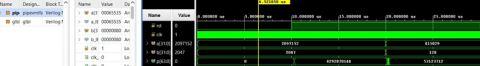
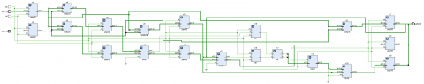
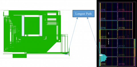
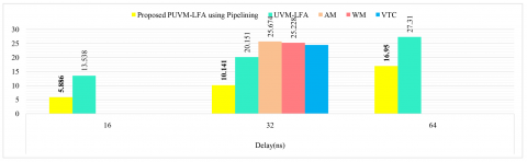
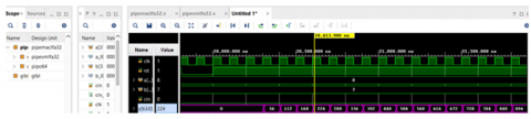
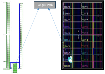
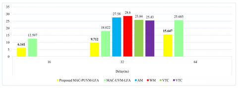
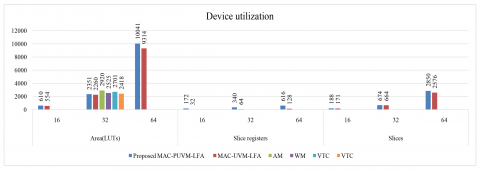
The suggested PUVM-LFA was also tested on the Virtex device to simulate and evaluate its functionality. Figure 7 shows the simulation results, RTL schematic, and device for the proposed 32-bit PUVM-LFA. The proposed PUVM-LFA's delays were compared with those of other current VMs and are listed in Tables 4-6. The comparison charts are presented in Figure 8. The comparison shows that the UVM-LFA improved combinational delay by 21.51%, 20.12%, and 17.61% for 32-bit width compared to AM, WM, and VTC, respectively, while the proposed PUVM-LFA reduced it by 49.67%, 60.50%, 59.80%, and 58.54% for 32-bit width compared to UVMLFA, AM, WM, and VTC, respectively, and reduced it by 37.93% and 56.52% for 64 and 16-bit width, respectively, as compared to UVMLFA. The area was reduced by 13.33% in PUVM-LFA for 32-bit when compared to AM, and reduced by 23%, 9.66%, and 5.44% in UVM-LFA when compared to AM, WM, and VTC. Because of pipelining, the device utilizations (LUTs, Slice registers, and Slices) are increased.
Table 2. Delay comparison of VMs [Kintex 7]
|
No of Bits |
4 |
8 |
16 |
32 |
|
Proposed PUVM-LFA using Pipelining |
3.876 |
4.114 |
5.974 |
10.481 |
|
Booth based VM (BB-VM) [12] |
- |
6.567 |
8.768 |
18.486 |
|
Booth with 4Mux based VM (B4M-VM) [12] |
- |
6.394 |
8.571 |
18.275 |
|
CS Multiplier based VM(CSM-VM) [12] |
3.888 |
4.116 |
7.856 |
18.112 |
|
CS Multiplier with 4Mux based VM (CS4M-VM) [12] |
3.991 |
4.565 |
7.212 |
18.613 |
|
Square Architecture (SquA) [18] |
4.2 |
8.6 |
19.9 |
32.7 |
|
U-VM [19] |
6.8 |
10.7 |
22.16 |
51.09 |
|
QCA-based VM (QCA-VM) [19] |
5.04 |
8.95 |
18.92 |
38.9 |
Table 3. Delay comparison of VMs [Artix 7]
|
No of Bits |
4 |
8 |
16 |
|
Proposed PUVM-LFA using Pipelining |
3.994 |
4.119 |
5.388 |
|
Method -2 Hybrid Booth Vedic Radix8 (M2-HBVR-8) [9] |
- |
4.425 |
- |
|
Method -3 Hybrid Booth Vedic Radix8 (M3-HBVR-8) [9] |
- |
4.597 |
- |
|
AM using Conditional Sum Adder (AM-COSA) [10] |
5.343 |
7.894 |
10.693 |
|
AM using Carry Select Adder (AM-CSLA) [10] |
5.336 |
6.991 |
9.816 |
|
AM using Ripple Carry Adder (AM-RCA) [10] |
5.343 |
7.302 |
10.776 |
|
AM using Carry Save Adder (AM-CSA) [10] |
5.343 |
7.565 |
11.67 |
|
Booth Vedic Radix4 (BVR-4) [15] |
5.363 |
12.59 |
18.57 |
|
Booth Vedic Radix8 (BVR-8) [15] |
6.461 |
10.554 |
15.83 |
|
ModularVM (ModVM) [17] |
4.6 |
4.7 |
7.6 |
|
Floating point Multiplier (Fl0PM) [24] |
4.1 |
4.7 |
6.3 |
(a)
(b)
Figure 6. (a) Delay comparison chart of VMs [Kintex 7] (b) Delay comparison chart of VMs [Artix 7]
Table 4. Delay comparison of 64-bit VMs [Virtex]
|
VMs |
Delay (ns) |
Area (LUTs) |
Slice Registers |
Slices |
|
Proposed PUVM-LFA using Pipelining |
16.950 |
9682 |
489 |
2691 |
|
UVM-LFA |
27.731 |
8721 |
- |
2448 |
Table 5. Delay comparison of 32-bit VMs [Virtex]
|
Multipliers |
Delay (ns) |
Area (LUTs) |
Slice Registers |
Slices |
|
Proposed PUVM-LFA using Pipelining |
10.141 |
2348 |
276 |
678 |
|
UVM-LFA |
20.151 |
2086 |
- |
589 |
|
Array Method (AM) [2] |
25.674 |
2709 |
- |
- |
|
Wallace Method (WM) [2] |
25.228 |
2309 |
- |
- |
|
Vedic Type with Compressor (VTC) [2] |
24.457 |
2206 |
- |
- |
Table 6. Delay comparison of 16-bit VMs [Virtex]
|
VMs |
Delay (ns) |
Area (LUTs) |
Slice Registers |
Slices |
|
Proposed PUVM-LFA using Pipelining |
5.886 |
523 |
140 |
156 |
|
UVM-LFA |
13.538 |
524 |
- |
153 |
(a) Simulation result
(b) RTL schematic
(c) Implementation schematic and device
Figure 7. Proposed 32-bit PUVM-LFA
(a)
(b)
Figure 8. Comparison chart of VMs [Virtex] (a) Delay (b) Device utilization
The proposed MAC-PUVMLFA was also tested on a Virtex device to simulate and validate performance. It was also discovered that the MAC unit created with the recommended pipelined VM and the LFA adder had lower latency than both the VM with LFA and the current MAC units. Figure 9 shows the simulation results, RTL schematic, implementation schematic, and device for the proposed 32-bit MAC unit.
(a) Simulation result
(b) Schematic of RTL
(c) Implementation schematic, and device
Figure 9. Proposed 32-bit MAC-PUVM-LFA
Tables 7-9 compare 64-bit, 32-bit, and 16-bit MAC units, with comparison charts presented in Figure 10. The comparison highlights the improvement in MAC-UVM-LFA, with combinational delay achieved by the 34.66%, 36.99%, 30.26% and 29.13% for 32-bit width, and area was reduced by 22.60%, 10.50%, 16.33%, and 6.53% for 16-bit width, and it was reduced by 19.49%, 6.89%, 12.96%, and 2.77% for 32-bit width in MAC-PUVM-LFA as compared to AM, WM, VeM, and VTC, respectively. The delay was decreased by 46.11%, 64.79%, 66.04%, 62.41%, and 62.81% in Proposed MAC-PUVM-LFA for 32-bit Width as compared to MAC-UVM-LFA, AM, WM, VeM, and VTC, respectively, and was decreased by 39.08% and 55.58% for 64 and 16-bit width, respectively, as compared to MAC-UVM-LFA.
Table 7. Comparison of 64-bit MAC units [Virtex]
|
MAC Units |
Delay (ns) |
Area (LUTs) |
Slice Registers |
Slices |
|
Proposed MAC-PUVM-LFA |
15.647 |
10041 |
616 |
2850 |
|
MAC-UVM-LFA |
25.685 |
9314 |
128 |
2576 |
Table 8. Comparison of 32-bit MAC units [Virtex]
|
MAC Units |
Delay (ns) |
Area (LUTs) |
Slice Registers |
Slices |
|
Proposed MAC-PUVM-LFA |
9.792 |
2351 |
340 |
674 |
|
MAC-UVM-LFA |
18.022 |
2260 |
64 |
664 |
|
Array Method (AM) [2] |
27.58 |
2920 |
- |
- |
|
Wallace Method (WM) [2] |
28.6 |
2525 |
- |
- |
|
Vedic Method (VeM) [2] |
25.84 |
2701 |
- |
- |
Table 9. Comparison of 16-bit MAC units [Virtex]
|
MAC Units |
Delay (ns) |
Area (LUTs) |
Slice Registers |
Slices |
|
Proposed MAC-PUVM-LFA |
6.141 |
610 |
172 |
188 |
|
MAC-UVM-LFA |
12.597 |
554 |
32 |
171 |
(a) Delay
(b) Device utilization
Figure 10. Comparison chart of MAC units [Virtex]
6.2 ASIC implementation
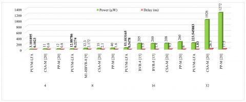
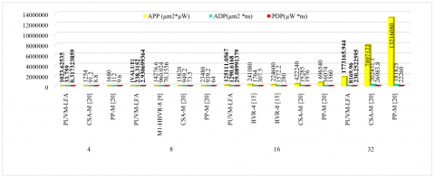
The suggested designs are built in an ASIC environment that includes TSMC 45 nm libraries. The design's efficiency is measured using VLSI metrics such as area, power, delay, ADP (area delay product), PDP (power delay product), and APP (area power product). A TCL script automates synthesis for operands of 4, 8, 16, and 32. Table 10 compares the results to state-of-the-art multipliers. Table 10 shows that the proposed PUVM-LFA architecture outperforms current designs in terms of speed, power, and area efficiency, resulting in faster performance while consuming less power.
Table 10. Performance comparison of multipliers in ASIC
|
No. of Bits |
Multipliers |
Area (µm2) |
Power (µw) |
Delay (ns) |
APP (µm2*µw) |
ADP (µm2*ns) |
PDP (µw*ns) |
|
4 |
Proposed PUVM-LFA using Pipelining |
330 |
3.101895 |
0.1023 |
1023.62535 |
33.759 |
0.31732386 |
|
CSA Multiplier (CSA-M) [20] |
114 |
11 |
0.8 |
1254 |
91.2 |
8.8 |
|
|
Parallel Prefix Multiplier (PP-M) [20] |
140 |
12 |
0.8 |
1680 |
112 |
9.6 |
|
|
8 |
Proposed PUVM-LFA using Pipelining |
1048 |
12.88786 |
0.2274 |
13506.4773 |
238.3152 |
2.93069936 |
|
Method -1 Hybrid Booth Vedic Radix8 (M1-HBVR-8) [9] |
442 |
32.3 |
2.172 |
14276.6 |
960.024 |
70.1556 |
|
|
CSA Multiplier (CSA-M) [20] |
452 |
35 |
2.1 |
15820 |
949.2 |
73.5 |
|
|
Parallel Prefix Multiplier (PP-M) [20] |
587 |
40 |
1.6 |
23480 |
939.2 |
64 |
|
|
16 |
Proposed PUVM-LFA using Pipelining |
2356 |
53.103165 |
0.5478 |
125111.057 |
1290.6168 |
29.0899138 |
|
Booth Vedic Radix4 (BVR-4) [15] |
1176 |
205 |
1.5 |
241080 |
1764 |
307.5 |
|
|
Booth Vedic Radix8 (BVR-8) [15] |
1123 |
200 |
1.4 |
224600 |
1572.2 |
280 |
|
|
CSA Multiplier (CSA-M) [20] |
2030 |
208 |
9.5 |
422240 |
19285 |
1976 |
|
|
Parallel Prefix Multiplier (PP-M) [20] |
2679 |
260 |
6 |
696540 |
16074 |
1560 |
|
|
32 |
Proposed PUVM-LFA using Pipelining |
7932 |
223.545883 |
1.03 |
1773165.94 |
8169.96 |
230.252259 |
|
CSA Multiplier (CSA-M) [20] |
7697 |
1026 |
26.3 |
7897122 |
202431.1 |
26983.8 |
|
|
Parallel Prefix Multiplier (PP-M) [20] |
10390 |
1272 |
17.5 |
13216080 |
181825 |
22260 |
Figure 11 shows a comparison chart of the PUVM-LFAs Delay, Power, ADP, APP, and PDP and delay. In comparison to CSA-M and PP-M, 45 nm PUVMLFA boosts power by 71.80% and 74.15%, delays by 87.21% and 87.21%, APP by 18.37% and 39.07%, ADP by 62.98% and 69.86%, and PDP by 96.39% and 96.99% with a bit-width of 4. While the bit-width of 8 results in a power gain of 60.10%, 63.18%, and 67.78%; delay improvements of 89.53%, 89.17%, and 85.79%; APP improvements of 5.39%, 14.62%, and 42.48%; and ADP improvements of 75.18%, 74.89%, and 74.63%, with PDP increases of 95.82%, 96.01%, and 95.42% in comparison to M1-HBVR-8, CSA-M, and PP-M, respectively. When compared to BVR-4, BVR-8, CSA-M, and PP-M, it has a power improvement of 74.10%, 73.45%, 74.47%, and 79.58%; a delay improvement of 63.48%, 60.87%, 94.23%, and 90.87%; APP improvements of 48.10%, 44.30%, 70.37%, and 82.04%; ADP improvements of 26.84%, 17.91%, 93.31%, and 91.97%; and PDP improvements of 90.54%, 89.61%, 98.53%, and 98.14% for 16 bits. When compared to CSA-M and PP-M, a bit-width of 32 resulted in power gains of 78.21% and 82.43%, delay improvements of 96.08% and 94.11%, APP improvements of 77.55% and 86.58%, ADP improvements of 96.96% and 95.11%, and PDP improvements of 99.15% and 98.97%.
(a) Power and delay
(b) APP, ADP, and PDP
Figure 11. Comparison chart of VMs [ASIC]
The power consumption breakdown of the PUVM-LFA architecture is presented in Table 11, which also illustrates the distribution of power among its various components. A deeper understanding of the design's power efficiency is made possible by this thorough analysis, which also identifies potential areas for improvement. Table 12 demonstrates that the proposed MAC-PUVM-LFA outperforms the MAC-UVM-LFA in two key aspects: greater speed and lower power consumption.
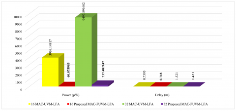
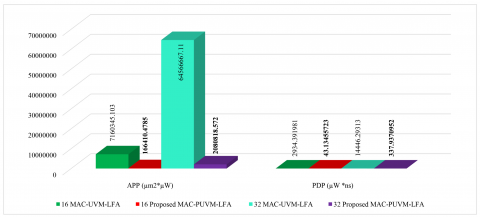
Figure 12 presents a comparison chart. In comparison to MAC-UVM-LFA, 45 nm MAC-PUVM-LFA improved power by 98.49% and 97.50%, delay by 2.88% and 6.44%, APD by 97.68% and 96.78%, and PDP by 98.53% and 97.66% for bit widths of 16 and 32 bits, respectively. A comparison of the power consumption breakdown for the MAC-UVM-LFA and MAC-PUVM-LFALFA architectures is presented in Table 13, facilitating a comparison of the potential benefits between the two designs and their power efficiency.
Table 11. Power comparison of PUVM-LFA units in ASIC
|
No. of Bits |
Internal Power (µw) |
Switching Power (µw) |
Leakage Power (µw) |
Total Power (µw) |
|
4 |
0.136546 |
0.105881 |
2.859467 |
3.101895 |
|
8 |
0.334415 |
0.261126 |
12.292320 |
12.88786 |
|
16 |
1.159820 |
1.094074 |
50.849270 |
53.103165 |
|
32 |
4.355157 |
1.772958 |
217.417770 |
223.545883 |
Table 12. Performance comparison of MAC units in ASIC
|
No. of Bits |
MAC Units |
Area (µm2) |
Power (µw) |
Delay (ns) |
APP (µm2*µw) |
ADP (µm2*ns) |
|
16 |
MAC-UVM-LFA |
1804 |
3969.14917 |
0.7393 |
7160345.103 |
2934.391981 |
|
Proposed MAC-PUVM-LFA |
2770 |
60.075985 |
0.718 |
166410.4785 |
43.13455723 |
|
|
32 |
MAC-UVM-LFA |
6798 |
9497.891602 |
1.521 |
64566667.11 |
14446.29313 |
|
Proposed MAC-PUVM-LFA |
8762 |
237.482147 |
1.423 |
2080818.572 |
337.9370952 |
(a) Power and delay
(b) APP, ADP, and PDP
Figure 12. Comparison chart of MAC units [ASIC]
Table 13. Power comparison of MAC units in ASIC
|
No. of Bits |
MAC Units |
Internal Power (µw) |
Switching Power (µw) |
Leakage Power (µw) |
Total Power (µw) |
|
16 |
MAC-UVM-LFA |
2071.610840 |
1842.936279 |
54.602009 |
3969.14917 |
|
Proposed MAC-PUVM-LFA |
1.453540 |
1.301418 |
57.321026 |
60.075985 |
|
|
32 |
MAC-UVM-LFA |
8848.806641 |
432.256195 |
216.829041 |
9497.891602 |
|
Proposed MAC-PUVM-LFA |
4.900466 |
2.256447 |
230.325226 |
237.482147 |
The proposed MAC unit, leveraging the Ladner-Fischer adder (LFA) in a Vedic structure with pipelining, demonstrates significant improvements in speed and power efficiency compared to conventional methods. This design's impact on real-time digital signal processing systems, IoT processors, and distributed computing architectures is substantial, enabling fast processing speeds and efficient performance. Potential applications include FIR, IIR, and other digital signal processing frameworks, as well as emerging technologies like 5G communication and IoT edge devices. Future work will focus on scaling the design for more than 64 bits and exploring application-level tests, such as image processing and neural network acceleration, to further validate its efficiency and versatility. This scalability and adaptability position the proposed MAC unit as a promising solution for next-generation computing systems.
I would like to express my sincere gratitude to my supervisor, Dr. Karthy/Associate Professor, Department of Electronics and Engineering, Dhanalakshmi Srinivasan University, Trichy, for their invaluable guidance and support throughout this research.
|
A |
First input of addition |
|
B |
Second input of addition |
|
C |
Carry input |
|
G |
Carry Generate |
|
P |
Carry Propagate |
|
S |
Sum of Addition |
|
Subscripts |
|
|
i |
Ranges from 0 to n |
[1] Dinesh, K.B.R., Vinoth, R., Kasyap, M. (2023). Design and implementation of high speed 32-bit MAC unit. Journal of Physics Conference Series, 2571(1): 012027. https://doi.org/10.1088/1742-6596/2571/1/012027
[2] Nagaraju, N., Ramesh, S.M. (2018). Implementation of high speed and area efficient MAC unit for industrial applications. ClusterComputing, 22(S2): 4511-4517. https://doi.org/10.1007/s10586-018-2060-z
[3] Babu, E.V., Talasila, S., Divya, N., Deva, S.S., Vani, C. (2023). Analysis of low-delay in 64-bit Vedic multiplier based MAC unit. In 2023 International Conference for Advancement in Technology (ICONAT), Goa, India, pp. 1-6. https://doi.org/10.1109/ICONAT57137.2023.10080612
[4] Harish, B., Rukmini, M.S.S., Sivani, K. (2021). Design of MAC unit for digital filters in signal processing and communication. International Journal of Speech Technology, 25(3): 561-565. https://doi.org/10.1007/s10772-021-09824-0
[5] Lilly, K., Nagaraj, S., Manvitha, B., Lekhya, K. (2020). Analysis of 32-bit Multiply and Accumulate unit (MAC) using Vedic Multiplier. In 2020 International Conference on Emerging Trends in Information Technology and Engineering (ic-ETITE), Vellore, India, pp. 1-4. https://doi.org/10.1109/ic-etite47903.2020.413
[6] Chhabra, A., Dhanoa, J. (2020). A design approach for mac unit using Vedic multiplier. In 2020 5th IEEE International Conference on Recent Advances and Innovations in Engineering (ICRAIE), Jaipur, India, pp. 1-5. https://doi.org/10.1109/icraie51050.2020.9358368
[7] Camus, V., Enz, C., Verhelst, M. (2019). Survey of precision-scalable multiply-accumulate units for neural-network processing. In Proceedings of the IEEE International Conference on Artificial Intelligence Circuits and Systems (AICAS), Hsinchu, Taiwan, pp. 57-61. https://doi.org/10.1109/aicas.2019.8771610
[8] Ahmed, H.O., Ghoneima, M., Dessouky, M. (2018). Concurrent MAC unit design using VHDL for deep learning networks on FPGA. In Proceedings of the IEEE Symposium on Computer Applications Industrial Electronics (ISCAIE), Penang, Malaysia, pp. 31-36. https://doi.org/10.1109/iscaie.2018.8405440
[9] Kalaiselvi, C.M., Sabeenian, R.S. (2025). Exploration of low area-high speed by hybrid method of Radix-8 Booth encoding and Vedic multiplier. Analog Integrated Circuits and Signal Processing, 122(3): 37. https://doi.org/10.1007/s10470-025-02339-7
[10] Chowdam, V.S., Potladurty, S.B., Karipireddy, P.R. (2025). Design and evaluation of clock-gating-based approximate multiplier for error-tolerant applications. Memories - Materials Devices Circuits and Systems, 9: 100123. https://doi.org/10.1016/j.memori.2025.100123
[11] Thamizharasan, V., Parthipan, V. (2024). Design of efficient binary multiplier architecture using hybrid compressor with FPGA implementation. Scientific Reports, 14(1): 8492. https://doi.org/10.1038/s41598-024-58482-0
[12] Kalaiselvi, C.M., Sabeenian, R.S. (2024). Design of area-speed efficient Anurupyena Vedic multiplier for deep learning applications. Analog Integrated Circuits and Signal Processing, 119(3): 521-533. https://doi.org/10.1007/s10470-024-02255-2
[13] Banumathi, J., Karthy, G. (2024). Analysis of Vedic multipliers using various adders and reversible logic– Review. In 2024 International Conference on Integration of Emerging Technologies for the Digital World (ICIETDW), Chennai, India, pp. 1-6. https://doi.org/10.1109/icietdw61607.2024.10939712
[14] Shetkar, S., Koli, S. (2023). Area, power efficient Vedic multiplier architecture using novel 4:2 compressor. Sādhanā, 48(4): 216. https://doi.org/10.1007/s12046-023-02274-1
[15] Kalaiselvi, C.M., Sabeenian, R.S. (2023). A modular technique of booth encoding and Vedic multiplier for low-area and high-speed applications. Scientific Reports, 13(1): 22379. https://doi.org/10.1038/s41598-023-49913-5
[16] Sathya Priya, S., Reddy, C.D.K., Reddy, S.R., Murugan, C.A. (2022). Implementation of multiplier using Vedic mathematics. Materials Today Proceedings, 65: 3921-3926. https://doi.org/10.1016/j.matpr.2022.04.1021
[17] Bianchi, V., De Munari, I. (2020). A modular Vedic multiplier architecture for model-based design and deployment on FPGA platforms. Microprocessors and Microsystems, 76: 103106. https://doi.org/10.1016/j.micpro.2020.103106
[18] Reddy, B.N.K. (2020). Design and implementation of high performance and area efficient square architecture using Vedic Mathematics. Analog Integrated Circuits and Signal Processing, 102: 501-506. https://doi.org/10.1007/s10470-019-01496-w
[19] Reddy, B.N.K., Vani, B.V., Lahari, G.B. (2020). An efficient design and implementation of Vedic multiplier in quantum-dot cellular automata. Telecommunication Systems, 74: 487-496. https://doi.org/10.1007/s11235-020-00669-7
[20] Elango, S., Sampath, P. (2020). Implementation of high-performance hierarchy-based parallel signed multiplier for cryptosystems. Journal of Circuits, Systems and Computers, 29(13): 2050214. https://doi.org/10.1142/s021812662050214x
[21] Sona, M.K., Somasundaram, V. (2020). Vedic multiplier implementation in VLSI. Materials Today Proceedings, 24: 2219-2230. https://doi.org/10.1016/j.matpr.2020.03.748
[22] Savji, A., Oza, S. (2020). Design and implementation of Vedic Multiplier. International Journal of Recent Technology and Engineering (IJRTE), 8(6): 3142-3145. https://doi.org/10.35940/ijrte.f8808.038620
[23] Sivanandam, K., Kumar, P. (2019). Design and performance analysis of reconfigurable modified Vedic multiplier with 3-1-1-2 compressor. Microprocessors and Microsystems, 65: 97-106. https://doi.org/10.1016/j.micpro.2019.01.002
[24] Gowreesrinivas, K.V., Samundiswary, P. (2017). Comparative analysis of single precision floating point multiplication using compressor techniques. In 2017 International Conference on Wireless Communications, Signal Processing and Networking (WiSPNET), Chennai, India, pp. 2428-2433. https://doi.org/10.1109/wispnet.2017.8300196
[25] Rahnamaei, A., Fatin, G.Z. (2018). High speed 16×16 bit booth multiplier based on novel 4-2 compressor structure. In 2018 1st International Conference on Advanced Research in Engineering Sciences (ARES), Dubai, United Arab Emirates, pp. 1-5. https://doi.org/10.1109/aresx.2018.8723266
[26] Mahammad, M.A., Uppala, A.R., Prasad, S.R., Marouthu, A. (2024). Performance analysis of parallel prefix adders developed with field programmable gate array technology. International Journal of Reconfigurable and Embedded Systems (IJRES), 14(1): 109-116. https://doi.org/10.11591/ijres.v14.i1.pp109-116
[27] Brzozowski, I. (2024). Comparative analysis of dynamic power consumption of parallel Prefix Adder. ACM Transactions on Design Automation of Electronic Systems, 29(3): 1-22. https://doi.org/10.1145/3651984
[28] Dubey, S., Verma, G. (2020). Analysis of basic adder with parallel prefix adder. In 2020 First IEEE International Conference on Measurement, Instrumentation, Control and Automation (ICMICA), Kurukshetra, India, pp. 1-6. https://doi.org/10.1109/icmica48462.2020.9242842
[29] Gauhar, S., Sharif, A., Alam, N. (2020). Comparison of parallel prefix adders based on FPGA & ASIC implementations. In 2020 IEEE Students Conference on Engineering & Systems (SCES), Prayagraj, India, pp. 1-6. https://doi.org/10.1109/sces50439.2020.9236737
[30] Thakur, G., Sohal, H., Jain, S. (2020). Design and analysis of high-speed parallel prefix adder for digital circuit design applications. In 2020 International Conference on Computational Performance Evaluation (ComPE), Shillong, India, pp. 95-100. https://doi.org/10.1109/compe49325.2020.9200064
[31] Banumathi, J., Karthy, G. (2025). Performance analysis of high-speed parallel prefix adders for arithmetic applications. Journal of Electronics and Informatics, 7(3): 191-205. https://doi.org/10.36548/jei.2025.3.001
[32] Perumal, V.K., Jayabalan, R., Krishnan, T., Selvaraj, D. (2025). Efficient address generator architectures for IEEE 802.16e WiMAX deinterleaver based on SPAM approach. Analog Integrated Circuits and Signal Processing, 124(3): 67. https://doi.org/10.1007/s10470-025-02477-y