Khushi Banarjee![]() | Aruna Pathak
| Aruna Pathak![]() | Chittajit Sarkar
| Chittajit Sarkar![]() | Chandan Kumar Choubey*
| Chandan Kumar Choubey*![]()
© 2024 The authors. This article is published by IIETA and is licensed under the CC BY 4.0 license (http://creativecommons.org/licenses/by/4.0/).
OPEN ACCESS
This research article presents the systematic development of a current-mode-based active comb filter designed to mitigate the undesirable PLI (power line interference) and its harmonics contaminating biomedical signals. The filter is designed using the latest current-mode Analog Building Block (ABB), specifically Voltage Differencing Gain Amplifiers (VDGA). This filter effectively suppresses the 50Hz PLI and reduces the odd consecutive harmonics of the 50Hz PLI, including the third harmonic at 150Hz, the fifth harmonic at 250Hz, and the seventh harmonic at 350Hz. In this design, we employ 'n' VDGAs as active components and '2n' capacitors as passive components to suppress 'n' frequencies. The active and passive components used in this filter are significantly fewer in number compared to similar filter designs in existing literature. Moreover, the filter can be electronically tuned for a specific pole frequency and quality factor value using the VDGA's bias currents. It's important to note that the pole frequency and the quality factor can be independently tuned owing to their orthogonal relationship. In simulation, the proposed filter demonstrates a notch depth of -42.9dB and a total harmonic distortion (THD) of -83dB, indicating its effectiveness in attenuating the pole frequency. The filter's design is simulated using a 0.18µm CMOS process technology and the macro-model of the MAX435 IC in the PSPICE simulator to validate its functionality and feasibility. Furthermore, a non-ideal analysis of the filter's performance has been conducted, considering real VDGAs exhibiting non-idealities such as transconductance gain errors and parasitics on their ports. Finally, the overall performance of this filter is compared based on various parameters, including the technology used, the number of active and passive components, supply voltage, the number of pole frequencies attenuated, notch depth, and THD, in comparison with existing comb and notch filters in the literature. The filter's performance and simplicity make it a promising choice in demanding biomedical detection systems.
comb filter, biomedical signals, power line interference, voltage differencing gain amplifier
Healthcare professionals rely on biomedical equipment to diagnose and treat patients, recording critical biomedical signals such as electrocardiograms (ECG) [1], electroencephalograms (EEG) [2], and electromyograms (EMG) [3]. These signals are physical and physiological indicators of body functions in real-time. Biomedical signals play a vital role in diagnosing and monitoring health conditions, providing valuable information about one's physiological, pathophysiological, and emotional states. These signals typically contain significant low-frequency components, ranging from several millihertz to several hundreds of hertz, with low amplitudes, often in the range of tens of microvolts to several millivolts.
For example, the ECG signal exhibits amplitudes between 100$\mu \mathrm{V}$ and 5mV, with varying frequencies in the range of 10-200Hz [1]. Similarly, the basic brain signal consists of four brain wave bands-$\delta$ (1-4Hz), $\theta$ (4-8Hz), $\alpha$ (8-13Hz), and $\beta$ (13-40Hz)-constituting the EEG signal. These waves manifest as continuous oscillating curves with weak amplitudes ranging from 2 to 200$\mu \mathrm{V}$ [2].
However, these signals are often susceptible to various types of noise, including instrumentation noise, muscle contractions, electrosurgical interference, baseline drift, motion artifacts, electrode contact issues, and Power-Line Interference (PLI) [4]. These noise sources can compromise the authenticity of biomedical signals, potentially leading to misinterpretations and false alarms. Notably, PLI at 50Hz or 60Hz and its harmonics are the most common noise sources that significantly impact biomedical signals [5].
To address the noise issues in biomedical signals, two commonly employed methods are: 1) A strategy based on the Signal Quality Index (SQI) to assess the clinical acceptability of recorded biomedical signals and 2) An approach based on denoising to reduce noise in biomedical signal recordings [6-11].
Signal Quality Index (SQI) Method: Before feature extraction, the quality of biomedical signals is assessed using various signal quality evaluation techniques. An extensive collection of SQIs is computed from the raw biomedical signal and physiological characteristics. These SQIs are then integrated or used as weighting variables to reduce false alarms in most biomedical equipment.
However, it's important to note that the effectiveness of SQI methods depends on factors such as the dataset, measurement parameters, and threshold selection logic. Additionally, the accuracy of signal quality predictions can be affected by labeling techniques, and the diversity of datasets also plays a significant role.
A method based on denoising: The elimination of power-line interference (PLI) has been addressed by several authors using both digital and analog filters. Many studies have documented various techniques employing different kinds of analog filters to eliminate or attenuate the 50Hz/60Hz signal along with its odd harmonics since analog filters are better suited for real-time processing [12-33]. Such analog filters, designed to notch out multiple frequencies simultaneously, are called comb filters due to the comb shape of the frequency response.
An active comb filter, based on operational amplifiers (op-amps), is introduced in the research [12] to eliminate 60Hz power line interference (PLI), while a similar approach is applied in the research [13] to address 50Hz PLI. Authors [14] also employ op-amps as an active block to mitigate 60Hz PLI and its three odd harmonics at 180Hz, 300Hz, and 420Hz. A notch filter utilizing the second-generation current conveyor (CCII) in 0.35$\mu \mathrm{m}$ CMOS technology is designed to notch out 50Hz interference [15].
Further, Ranjan et al. [16] present an operational transconductance amplifier (OTA) and capacitor-based comb filter circuit, implemented in 0.5$\mu \mathrm{m}$ CMOS technology, tested against 60Hz PLI and its three odd harmonics. The work [17] introduces a comb filter circuit using $\text { CCII+ }$ and IC AD844 in 0.18$\mu \mathrm{m}$ CMOS technology to eliminate undesirable 60Hz PLI and its three odd harmonics at 180Hz, 300Hz, and 420Hz.
In the domain of EEG applications, Qian et al. [18] propose an OTA-C-based low-pass notch filter in 0.35$\mu \mathrm{m}$ CMOS technology. Additionally, for cardiac activity detection, Lee and Cheng [19] introduce another OTA-C filter using 0.18$\mu \mathrm{m}$ CMOS technology. Moreover, Alzaher et al. [20] suggest an op-amp-based power-line removal filter in CMOS 0.18$\mu \mathrm{m}$ for biomedical potential acquisition systems.
To tackle 50Hz PLI and its three odd harmonics (150Hz, 250Hz, and 350Hz), Paul et al. [21] propose a $\text { CCII } \pm$ based filter, where CCIIs are designed using both the macro-model of IC AD844 and dynamic threshold-voltage metal oxide semiconductor (DTMOS) technology. A digitally programmable OTA-based filter is presented in the research [22] to minimize the impact of 50Hz PLI and its 3rd harmonics (150Hz).
For processing biomedical signals at front-ends, Machha Krishna and Laxminidhi [23] introduce a Butterworth transconductor-capacitor (gm-C) filter based on OTA. A multiple-output fully differential OTA (MOFD OTA)-based filter is designed to process electromyography (EMG) signals [24].
Notch filters to eliminate 60Hz frequency are proposed in the studies [25, 26] using op-amps, with the latter employing 65nm CMOS technology. Employing 90nm CMOS technology, the authors [27] introduce an OTA-C filter structure for notch and lowpass filtering to suppress the 50Hz frequency. Furthermore, Zhang et al. [28] propose another OTA-based low-pass filter and a notch filter in 0.18$\mu \mathrm{m}$ CMOS technology.
A multiple-output OTA (MO-OTA)-based notch filter in 0.25$\mu \mathrm{m}$ CMOS technology is suggested to remove PLI [29]. Voltage-mode biquad filters based on voltage differencing differential input buffered amplifiers (VD-DIBA) are proposed for biosensor applications [30]. Similarly, Kumngern et al. [31] suggest using a low-voltage differential difference transconductance amplifier (DDTA) to remove PLI for biosensor applications.
For advanced configurations, Kumngern et al. [32] implement a multiple-input, multiple-output (MIMO) OTA-based notch filter using 0.18$\mu \mathrm{m}$ DTMOS technology. Finally, a multiple-input differential difference transconductance amplifier (MI-DDTA)-based notch filter is proposed in 0.18$\mu \mathrm{m}$ CMOS technology [33].
The existing comb filters present several noteworthy limitations. Firstly, the active comb filter is confined to the removal of a single frequency, i.e., only the fundamental frequency of the PLI [12, 13, 15, 18, 19, 23-30, 33]. Furthermore, using excessive active blocks and passive components in the circuit design, as observed in studies [12-33], results in complex circuits, increasing the chip area and power consumption. Moreover, the design's dependency on resistors contributes to a larger chip area [12-15, 17, 20, 21, 25, 28, 30-31, 33]. Another critical drawback is the absence of an examination and mitigation strategy for the non-idealities inherent in the active block [13, 15-18, 21-27, 29]. Lastly, the structures outlined in studies [12-33] exhibit elevated levels of total harmonic distortion (THD), emphasizing that lower THD values are indicative of superior filter performance.
This literature survey provides an in-depth exploration of comb filters employed in signal-processing applications. Specifically, various comb filter designs and implementations are investigated for their efficacy in addressing power line interference (PLI) issues. The surveyed literature showcases a diverse range of comb filter configurations, emphasizing their application in mitigating interference at 60Hz and 50Hz, along with their respective harmonics.
Due to the intrinsic qualities of current-mode active blocks, such as simplified design, better precision, stronger linearity, wider bandwidth, higher slew rate, greater dynamic range, and the capacity to operate at low voltage, they have drawn much interest from academics in recent years. One of the most adaptable and practical current-mode building blocks is the VDGA (voltage differencing gain amplifier) [34-37].
This paper introduces a novel analog comb filter, leveraging a notch filter approach to mitigate or reduce Power Line Interference (PLI) in low-frequency biomedical signals, including ECG, EEG, and EMG signals. Notably, the proposed circuit exhibits versatility, extending its applicability to diverse scenarios. Beyond its primary use in minimizing PLI in biomedical signals, the circuit can effectively contribute to tasks such as mitigating acoustic feedback oscillations in voice amplification systems and estimating pitch in audio signals within noisy environments. The core design of the filter exclusively features Voltage Differencing Gain Amplifiers (VDGAs) and capacitors, establishing it as a VDGA-based comb filter suitable for IC fabrication.
The significant novelties of the proposed design can be succinctly outlined as follows:
(a) Design of a simple comb filter exclusively comprised of VDGAs and capacitors.
(b) The proposed filter structure occupies less chip area as it does not require any resistor for its design.
(c) Achieving single-frequency notching with remarkable efficiency, utilizing only a single VDGA and two capacitors.
(d) For the blocking of n frequencies, the proposed design employs n VDGAs and 2n capacitors exclusively.
(e) The proposed filter effectively suppresses the effect of the 50Hz PLI along with odd harmonics of the 50Hz PLI, such as 150Hz, 250Hz, and 350Hz.
(f) The filter's parameters, such as the pole frequencies and the quality factors, can be electronically controlled and independently tuned using the VDGA's bias currents.
(h) The proposed structure offers a -42.9dB notch depth sufficient to eliminate the undesired frequency.
(i) The proposed structure achieved the lowest THD of -83dB compared with available structures.
(j) The proposed notch filter is well suited for analog front-end devices for biomedical signal detection, such as EEG, EMG, and ECG.
This research paper is organized into seven distinct sections. Section 2 provides a concise overview of the modern active block, VDGA, which constitutes the fundamental building block in the proposed comb filter. Section 3 delves into the realization of the proposed comb filter by utilizing VDGA. The workability of the proposed design is rigorously assessed and validated in Section 4, employing both the 0.18$\mu \mathrm{m}$ CMOS technology process parameters of TSMC and the macro-model of the IC MAX435. Non-ideality and sensitivity analysis of the proposed comb filter are thoroughly expounded upon in Section 5. Section 6 compares the performance of the proposed comb filter with existing circuits documented in the literature. Finally, Section 7 concludes this paper, encapsulating the key findings and insights derived from the study.
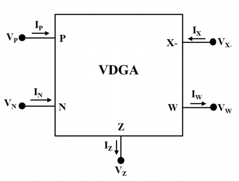
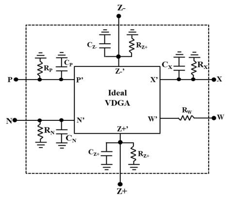
This section delves into a versatile current-mode building block known as the VDGA, given that the proposed filters leverage VDGA as active components. With the growing interest in ASP (Analog Signal Processing) and ASG (Analog Signal Generating) circuits, there has been a heightened focus on establishing and synthesizing new electronically programmable ABBs. These current-mode ABBs, including the VDGA, are expected to outperform their voltage-mode operational amplifier counterparts. The VDGA is a five-terminal ABB featuring two input terminals (P and N) and three output terminals (Z, W, and X-), as illustrated in Figure 1. Notably, the input terminals, P and N, exhibit very high impedance, and similarly, the output terminals, Z and X-, possess high impedance. In contrast, the output terminal, W, has low impedance. The introduction of this ABB to the analog domain dates back to 2013 [38].
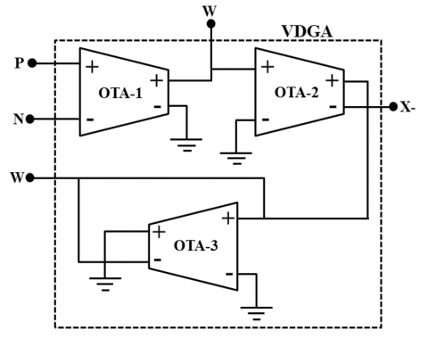
As illustrated in Figure 2, a VDGA is implemented using three OTAs, resulting in three transconductance gains. To analyze circuits based on VDGA, it is essential to understand the input and output terminal relationships, given in matrix form in (1). The terminal relationship outlined in (1) can be succinctly explained as (a) Input currents, IP and IN, are negligible since terminals P and N possess very high impedance. (b) The differential voltage, VP-VN, appears at the Z terminal in the current form as IZ, obtained by multiplying with the first transconductance, gmA. (c) The Z terminal voltage, VZ, undergoes multiplication with the second transconductance gain, gmB, resulting in its appearance at the X terminal in current form as IX. (d) A factor β amplifies the VZ voltage at the Z terminal and emerges at the W terminal. A possible symbolic implementation of a VDGA using three OTAs is shown in Figure 2 [39].
$\left[ \begin{matrix}
\begin{matrix}
{{I}_{P}} \\
{{I}_{N}} \\
\end{matrix} \\
{{I}_{Z}} \\
\begin{matrix}
\begin{matrix}
{{I}_{X}} \\
{{I}_{W}} \\
\end{matrix} \\
{{V}_{W}} \\
\end{matrix} \\
\end{matrix} \right]$=$\left[ \begin{matrix}
\begin{matrix}
0 & 0 \\
0 & 0 \\
{{g}_{mA}} & -{{g}_{mA}} \\
\end{matrix} & \begin{matrix}
0 & \begin{matrix}
0 & 0 \\
\end{matrix} \\
0 & \begin{matrix}
0 & 0 \\
\end{matrix} \\
0 & \begin{matrix}
0 & 0 \\
\end{matrix} \\
\end{matrix} \\
\begin{matrix}
0 & 0 \\
\end{matrix} & \begin{matrix}
{{g}_{mB}} & \begin{matrix}
0 & 0 \\
\end{matrix} \\
\end{matrix} \\
\begin{matrix}
\begin{matrix}
0 \\
0 \\
\end{matrix} & \begin{matrix}
0 \\
0 \\
\end{matrix} \\
\end{matrix} & \begin{matrix}
\begin{matrix}
-{{g}_{mB}} \\
\beta \\
\end{matrix} & \begin{matrix}
\begin{matrix}
0 \\
0 \\
\end{matrix} & \begin{matrix}
{{g}_{mC}} \\
0 \\
\end{matrix} \\
\end{matrix} \\
\end{matrix} \\
\end{matrix} \right]\left[ \begin{matrix}
\begin{matrix}
{{V}_{P}} \\
{{V}_{N}} \\
\end{matrix} \\
{{V}_{Z}} \\
\begin{matrix}
{{V}_{X}} \\
{{V}_{W}} \\
\end{matrix} \\
\end{matrix} \right]$ (1)
where, $\beta =\frac{{{g}_{mB}}}{{{g}_{mC}}}$.
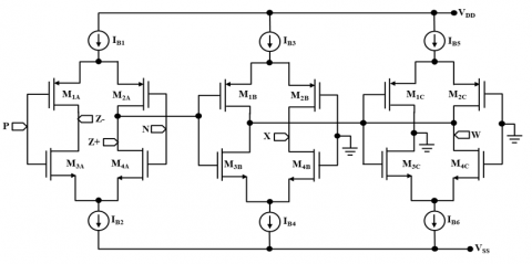
The CMOS architecture of a VDGA employing three Arbel-Goldminz transconductances (AGTs) [40] is depicted in Figure 3. In this configuration, the three AGTs are labeled as A, B, and C, each specifying their transconductance gain as follows:
${{g}_{mj}}=\frac{{{g}_{1j}}{{g}_{2j}}}{{{g}_{1j}}+{{g}_{2j}}}+\frac{{{g}_{3j}}{{g}_{4j}}}{{{g}_{3j}}+{{g}_{4j}}}$ (2)
where, ${{g}_{ij}}$(i=1, 2, 3, 4 and j=A, B, C) is each MOSFET’s transconductance gain. The transconductance gain of a MOSFET is expressed as:
${{g}_{ij}}=\sqrt{{{I}_{ij}}{{\mu }_{\left( n~or~p \right)}}Co{{x}_{\left( n~or~p \right)}}\left( \frac{W}{L} \right)ij}$ (3)
W, L, Iij, µ, and Cox maintain standard definitions here. The interrelation between (2) and (3) reveals that the transconductances can be electronically adjusted by varying their bias currents.
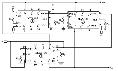
The OTA integrated circuit (IC) MAX435 is employed to construct the VDGA illustrated in Figure 2, as presented in Figure 4. Within this figure, the resistors, Rx, Ry, and Rz are placed across pins 3 and 5 of each IC. These resistors serve the purpose of regulating the transconductance gains (gmA, gmB, and gmC), consequently influencing the voltage gain ($\beta =\frac{{{g}_{mB}}}{{{g}_{mC}}}$), in accordance with the relationship ${{g}_{mj}}=\frac{4}{{{R}_{j}}}$, where j =A, B, and C. Additionally, resistors Rp1, Rp2, and Rp3, placed across pin 11 and ground, control the supply currents flowing through the ICs.
Figure 1. Schematic symbol of the VDGA
Figure 2. Implementation of VDGA using three OTAs
Figure 3. Realization of VDGA utilising CMOS AGTs
Figure 4. Realisation of VDGA utilising the OTA IC MAX435
Various analog approaches for designing a comb filter have been reported in the literatures [16-17, 21]. The comb filter is constructed using low Q (quality factor) RLC notch filters, incorporating OTA-based synthetic inductors [16]. Whereas, the methodologies for comb filter design are based on IBPFs (inverted bandpass filters) and APFs (all-pass filters), respectively [17, 21]. Upon scrutinizing these approaches, it becomes evident that the most straightforward and effective means of implementing a comb filter involves using high-Q RLC notch filters. Elevating the quality factor of a band reject/stop filter results in a notch filter capable of selectively attenuating or suppressing specific frequencies within a frequency spectrum.
The systematic realization starts with the analysis of the second-order passive notch filters. Circuit implementations of a series-LC and a parallel-LC notch filter are depicted in Figure 5. In the second-order passive series-LC notch filter, depicted in Figure 5(a), the input signal is fed to the resistor (R), and the output is obtained from a series arrangement of an inductor (L) and a capacitor (C). Conversely, in the second-order passive parallel-LC notch filter, the input is supplied to a parallel arrangement of an inductor (L) and a capacitor (C), and the output is derived across a resistor (R), as illustrated in Figure 5(b).
The standard analysis yields the transfer function of the series-LC notch filter in Figure 5(a) as:
$H\left( s \right)=\frac{{{V}_{out~}}\left( s \right)}{{{V}_{in}}\left( s \right)}=\frac{{{s}^{2}}+{}^{1}/{}_{LC}}{{{s}^{2}}+{}^{sR}/{}_{L}+{}^{1}/{}_{LC}}$ (4)
The parameters for the notch filter are defined as follows:
${{\omega }_{0}}=\frac{1}{\sqrt{LC}}$,${{f}_{0}}=\frac{1}{2\pi \sqrt{LC}}$, and $Q=\frac{1}{R}\sqrt{\frac{L}{C}}$ (5)
Examining the expression for Q in (5), it becomes evident that the Q value is consistently low for practical passive component values. Therefore, this type of filter is suitable for low-Q applications. An effective notch filter demands a narrow, deep stop band around the pole frequency. A High-Q Notch Filter (HQNF) is crucial to achieve these desired properties. Consequently, designing a notch filter with a high Q value is preferable. Thus, the inspiration for implementing an analog comb filter arose, utilizing an HQNF as the foundational circuit.
The transfer function of the series-LC notch filter illustrated in Figure 5(b) is derived through routine analysis:
$H\left( s \right)=\frac{{{V}_{out~}}\left( s \right)}{{{V}_{in}}\left( s \right)}=\frac{{{s}^{2}}+{}^{1}/{}_{LC}}{{{s}^{2}}+{}^{s}/{}_{RC}+{}^{1}/{}_{LC}}$ (6)
From (6), the filter parameters are determined as:
${{\omega }_{0}}=\frac{1}{\sqrt{LC}}$, ${{f}_{0}}=\frac{1}{2\pi \sqrt{LC}}~$, and $Q=R\sqrt{\frac{C}{L}}$ (7)
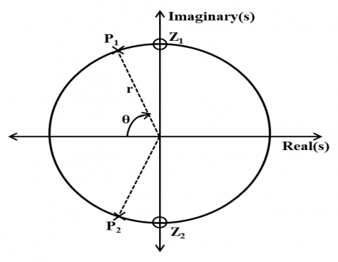
Observing the expression for Q in Eq. (7), it becomes evident that a high Q value can be achieved with practical passive component values. With this insight, we proceed to design a comb filter, incorporating this fundamental filter in the background. Utilizing the transfer function provided in Eq. (6), the locations of poles and zeros can be plotted in the s-domain, as illustrated in Figure 6.
These poles and zeroes can be expressed as:
${{P}_{1}}=-\frac{1}{2RC}+\frac{1}{2}\sqrt{{{\left( \frac{1}{RC} \right)}^{2}}-\frac{4}{LC}};~{{P}_{2}}=-\frac{1}{2RC}-\frac{1}{2}\sqrt{{{\left( \frac{1}{RC} \right)}^{2}}-\frac{4}{LC}}$; ${{Z}_{1}}=+\frac{j}{\sqrt{LC}}$; ${{Z}_{2}}=-\frac{j}{\sqrt{LC}}$ (8)
For an HQNF, the three essential requirements that the transfer function should exhibit are: (i) poles should be close to zeroes, (ii) a phase shift of -π/2 or π/2 should occur at the pole frequency, and (iii) zeros should be at the imaginary axis. The radius (r) and the angle (θ) in Figure 6 can be expressed as:
$r={{\omega }_{0}}$; θ =${{\tan }^{-1}}\sqrt{4{{Q}^{2}}-1}$ (9)
Observing (9), it is apparent that θ increases with an increase in the value of Q, indicating that the poles will move toward the zeros with an improvement in Q.
Substituting s= j$\omega $ in (6), the expression for phase can be obtained. The phase of H $(j\omega $) is expressed as:
$\angle H\left( j\omega \right)=-{{\tan }^{-1}}\frac{\omega {{\omega }_{0}}}{{{Q}_{0}}\left( {{\omega }_{0}}^{2}-{{\omega }^{2}} \right)}$ (10)
At the pole frequency (ω=ω0), the phase is $\angle H\left( j\omega \right)$=-π/2, fulfilling the second criterion of the notch filter. Additionally, the zeroes are located on the imaginary axis of the plot.
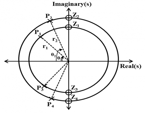
A cascading methodology is adopted to notch the n-number of frequencies, where the n-number of HQNFs are cascaded. To validate this methodology theoretically, two HQNFs are cascaded, as depicted in Figure 7, for notching two different frequencies. The transfer function of the two cascaded notch filters can be written as:
$H\left( s \right)=\frac{{{V}_{out~}}\left( s \right)}{{{V}_{in}}\left( s \right)}=\left( \frac{{{s}^{2}}+{}^{1}/{}_{{{L}_{1}}{{C}_{1}}}}{{{s}^{2}}+{}^{s}/{}_{{{R}_{1}}{{C}_{1}}}+{}^{1}/{}_{{{L}_{1}}{{C}_{1}}}} \right)\left( \frac{{{s}^{2}}+{}^{1}/{}_{{{L}_{2}}{{C}_{2}}}}{{{s}^{2}}+{}^{s}/{}_{{{R}_{2}}{{C}_{2}}}+{}^{1}/{}_{{{L}_{2}}{{C}_{2}}}} \right)$ (11)
Eq. (11) can be rewritten as:
$H\left( s \right)=\frac{{{V}_{out~}}\left( s \right)}{{{V}_{in}}\left( s \right)}=\frac{{{s}^{4}}+\left( {}^{1}/{}_{{{L}_{1}}{{C}_{1}}}+{}^{1}/{}_{{{L}_{2}}{{C}_{2}}}+{}^{1}/{}_{{{R}_{1}}{{C}_{1}}{{R}_{2}}{{C}_{2}}} \right){{s}^{2}}+{}^{1}/{}_{{{L}_{1}}{{C}_{1}}{{L}_{2}}{{C}_{2}}}}{\left( {{s}^{2}}+{}^{s}/{}_{{{R}_{1}}{{C}_{1}}}+{}^{1}/{}_{{{L}_{1}}{{C}_{1}}} \right)\left( {{s}^{2}}+{}^{s}/{}_{{{R}_{2}}{{C}_{2}}}+{}^{1}/{}_{{{L}_{2}}{{C}_{2}}} \right)}$ (12)
From (12), it can be observed that for larger values of Q1 and Q2, ${}^{1}/{}_{{{R}_{1}}{{C}_{1}}{{R}_{2}}{{C}_{2}}\ll }\left( {}^{1}/{}_{{{L}_{1}}{{C}_{1}}}+{}^{1}/{}_{{{L}_{2}}{{C}_{2}}} \right),~$then the transfer function can be expressed as:
$H\left( s \right)=\frac{{{V}_{out~}}\left( s \right)}{{{V}_{in}}\left( s \right)}=\frac{{{s}^{4}}+\left( {}^{1}/{}_{{{L}_{1}}{{C}_{1}}}+~{}^{1}/{}_{{{L}_{2}}{{C}_{2}}} \right){{s}^{2}}+{}^{1}/{}_{{{L}_{1}}{{C}_{1}}{{L}_{2}}{{C}_{2}}}}{\left( {{s}^{2}}+{}^{s}/{}_{{{R}_{1}}{{C}_{1}}}+{}^{1}/{}_{{{L}_{1}}{{C}_{1}}} \right)\left( {{s}^{2}}+{}^{s}/{}_{{{R}_{2}}{{C}_{2}}}+{}^{1}/{}_{{{L}_{2}}{{C}_{2}}} \right)}$ (13)
Figure 5. Circuits of (a) Series-LC notch filter (b) Parallel LC notch filter
Figure 6. Pole-zero plot of Figure 5(b)
Figure 7. Realization of comb filter for n=2
Figure 8. Pole-zero plot of Figure 7
From (13), the poles (P1, P2, P3, and P4) and zeroes (Z1, Z2, Z3, and Z4) can be expressed as:
${{P}_{1}}=-\frac{1}{2~{{R}_{1}}{{C}_{1}}}+\frac{1}{2}\sqrt{{{\left( \frac{1}{{{R}_{1}}{{C}_{1}}} \right)}^{2}}-\frac{4}{{{L}_{1}}{{C}_{1}}}}$; ${{P}_{2}}=-\frac{1}{2~{{R}_{1}}{{C}_{1}}}-\frac{1}{2}\sqrt{{{\left( \frac{1}{{{R}_{1}}{{C}_{1}}} \right)}^{2}}-\frac{4}{{{L}_{1}}{{C}_{1}}}}$; ${{P}_{3}}=-\frac{1}{2~{{R}_{2}}{{C}_{2}}}+\frac{1}{2}\sqrt{{{\left( \frac{1}{{{R}_{2}}{{C}_{2}}} \right)}^{2}}-\frac{4}{{{L}_{2}}{{C}_{2}}}}$; ${{P}_{4}}=-\frac{1}{2~{{R}_{2}}{{C}_{2}}}-\frac{1}{2}\sqrt{{{\left( \frac{1}{{{R}_{2}}{{C}_{2}}} \right)}^{2}}-\frac{4}{{{L}_{2}}{{C}_{2}}}}$; ${{Z}_{1}}=+\frac{j}{\sqrt{{{L}_{1}}{{C}_{1}}}}$; ${{Z}_{2}}=-\frac{j}{\sqrt{{{L}_{1}}{{C}_{1}}}}$; ${{Z}_{3}}=+\frac{j}{\sqrt{{{L}_{2}}{{C}_{2}}}}$, and ${{Z}_{4}}=-\frac{j}{\sqrt{{{L}_{2}}{{C}_{2}}}}$. (14)
The pole and zero locations in the s-domain are graphically represented in Figure 8. Substituting s= j$\omega $ into (13), the phase of H($j\omega $) is formulated as:
$\angle H\left( j\omega \right)=-{{\tan }^{-1}}\left[ \frac{\omega \left( \frac{{{\omega }_{1}}\omega _{2}^{2}}{{{Q}_{1}}}+\frac{{{\omega }_{2}}\omega _{1}^{2}}{{{Q}_{2}}} \right)-{{\omega }^{3}}\left( \frac{{{\omega }_{1}}}{{{Q}_{1}}}+\frac{{{\omega }_{2}}}{{{Q}_{2}}} \right)}{{{\omega }^{4}}-\left( \omega _{1}^{2}+\omega _{2}^{2} \right){{\omega }^{2}}+\omega _{1}^{2}\omega _{2}^{2}} \right]$ (15)
From (15), the phase is computed as: $\angle H\left( j\omega \right)=$-π/2 for ω =ω1 and $\angle H\left( j\omega \right)=$π/2 for ω=ω2. This analysis indicates that the cascaded filter depicted in Figure 7 can effectively notch two distinct frequencies.
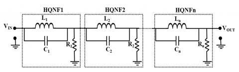
This approach can be extended to notch n-number of pole frequencies. For this purpose, n HQNFs are cascaded, as illustrated in Figure 9, forming what is commonly known as a "comb filter" due to its frequency response pattern. The overall transfer function of the filter in Figure 9 is derived by multiplying the transfer functions of each cascaded HQNF, as given in Eq. (16).
In the design, the pole frequencies of the HQNFs are strategically chosen to enable the comb filter to block the power-line frequency and its odd harmonics. For instance, if the comb filter is intended to filter out the undesired power-line interference (PLI) of frequency f1 and its odd harmonics f2, f3, ..., fn, the HQNFs are designed with pole frequencies corresponding to f1, f2, f3, and fn. This configuration results in an undistorted output signal VOUT after the comb filter rejects the undesirable frequencies.
Fabricating inductors for integrated circuits poses significant challenges due to the layer-oriented nature of most IC fabrication procedures. On-chip inductors also consume considerable chip space, and integrating passive resistance in ICs is impractical due to space constraints and power consumption. Consequently, the proposed comb filter is designed with a novel active element, the Voltage Differencing Gain Amplifier (VDGA), to streamline the implementation of the integrated circuit.
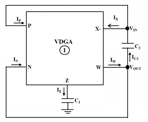
As discussed earlier, the HQNF serves as the fundamental building block of the proposed comb filter. Initially, an HQNF is devised using VDGA, as depicted in Figure 10, with its transfer function and parameters resembling those of the parallel-LC HQNF shown in Figure 5 (b).
$H\left( s \right)=\frac{{{V}_{out~}}\left( s \right)}{{{V}_{in}}\left( s \right)}=\left( \frac{{{s}^{2}}+{}^{1}/{}_{{{L}_{1}}{{C}_{1}}}}{{{s}^{2}}+{}^{s}/{}_{{{R}_{1}}{{C}_{1}}}+{}^{1}/{}_{{{L}_{1}}{{C}_{1}}}} \right)\left( \frac{{{s}^{2}}+{}^{1}/{}_{{{L}_{2}}{{C}_{2}}}}{{{s}^{2}}+{}^{s}/{}_{{{R}_{2}}{{C}_{2}}}+{}^{1}/{}_{{{L}_{2}}{{C}_{2}}}} \right)\left( \frac{{{s}^{2}}+{}^{1}/{}_{{{L}_{3}}{{C}_{3}}}}{{{s}^{2}}+{}^{s}/{}_{{{R}_{3}}{{C}_{3}}}+{}^{1}/{}_{{{L}_{3}}{{C}_{3}}}} \right)\ldots \ldots \left( \frac{{{s}^{2}}+{}^{1}/{}_{{{L}_{n}}{{C}_{n}}}}{{{s}^{2}}+{}^{s}/{}_{{{R}_{n}}{{C}_{n}}}+{}^{1}/{}_{{{L}_{n}}{{C}_{n}}}} \right)$ (16)
Figure 9. Realization of comb filter using n-number of HQNFs
Figure 10. Realization of HQNF using VDGA
To determine the transfer function, the circuit illustrated in Figure 10 is analysed as follows:
Utilising the terminal-relationship of the VDGA given in (1), the current IZ can be expressed as ${{I}_{Z}}={{g}_{mA}}\left( {{V}_{P}}-{{V}_{N}} \right)$. Consequently, the voltage at the terminal Z (VZ) is given by:
${{V}_{Z}}=\frac{{{I}_{Z}}}{s{{C}_{1}}}=\frac{{{g}_{mA}}\left( {{V}_{IN}}-{{V}_{OUT}} \right)}{s{{C}_{1}}}$ (17)
Again, employing (1), the current through terminal W of the VDGA can be expressed as ${{I}_{W}}={{g}_{mB}}{{V}_{Z}}-{{g}_{mC}}{{V}_{W}}$. Additionally, the current through terminal N is zero, i.e., ${{I}_{N}}$= 0. From Figure 10, the current through capacitor C2 is determined as ${{I}_{C2}}=s{{C}_{2}}\left( {{V}_{OUT}}-{{V}_{IN}} \right).$ Applying Kirchhoff’s current law (KCL) at node VOUT yields:
${{I}_{W}}={{I}_{C2}}+{{I}_{N}}={{I}_{C2}}+0={{I}_{C2}}$ (18)
Now, (18) can be rearranged as:
${{g}_{mB}}{{V}_{Z}}-{{g}_{mC}}{{V}_{W}}=s{{C}_{2}}\left( {{V}_{OUT}}-{{V}_{IN}} \right)$ (19)
By substituting ${{V}_{Z}}$ from (17) and using ${{V}_{W}}={{V}_{OUT}}$ from Figure 10, (19) is further rewritten as:
${{g}_{mB}}\left[ \frac{{{g}_{mA}}\left( {{V}_{IN}}-{{V}_{OUT}} \right)}{s{{C}_{1}}} \right]-{{g}_{mC}}{{V}_{OUT}}=s{{C}_{2}}\left( {{V}_{OUT}}-{{V}_{IN}} \right)$ (20)
Rearranging (20) yields the transfer function of the HQNF as:
$H\left( s \right)=\frac{{{V}_{OUT}}\left( s \right)}{{{V}_{IN}}\left( s \right)}=\frac{{{s}^{2}}+\frac{{{g}_{mA}}{{g}_{mB}}}{{{C}_{1}}{{C}_{2}}}~}{{{s}^{2}}+s\frac{{{g}_{mC}}}{{{C}_{2}}}+\frac{{{g}_{mA}}{{g}_{mB}}}{{{C}_{1}}{{C}_{2}}}}$ (21)
The coefficients of the transfer functions of the VDGA-based HQNF and the passive HQNF given in (6) and (21), respectively, are compared to derive equivalent expressions for the passive elements R, L, and C of Figure 5 (b) in terms of the transconductances ((gmA, gmB, and gmC) of the VDGA and the capacitors used (C1 and C2) in Figure 10 as follows:
$R=\frac{1}{{{g}_{mC}}}$, $L=\frac{{{C}_{1}}}{{{g}_{mA}}{{g}_{mB}}}$, and $C={{C}_{2}}$ (22)
From (22), it can be observed that the resistance R and the inductance L values depend on the value of transconductances. As these transconductances can be varied by varying the bias current of the VDGA, as given in (2) and (3), the values of R and L can be changed by adjusting the bias current of the VDGA. The pole frequency and the quality factor of the VDGA-based HQNF can be rewritten using (6) and (22) as follows:
${{f}_{0}}=\frac{1}{2\pi \sqrt{LC}}=\frac{1}{2\pi }\sqrt{\frac{{{g}_{mA}}{{g}_{mB}}}{{{C}_{1}}{{C}_{2}}}}$ and $Q=R\sqrt{\frac{C}{L}}=\frac{1}{{{g}_{mC}}}\sqrt{\frac{{{C}_{1}}{{C}_{2}}}{{{g}_{mA}}{{g}_{mB}}}}$ (23)
$H\left( s \right)=\frac{{{V}_{out~}}\left( s \right)}{{{V}_{in}}\left( s \right)}=\left( \frac{{{s}^{2}}+\frac{{{g}_{mA1}}{{g}_{mB1}}}{{{C}_{1}}{{C}_{2}}}~}{{{s}^{2}}+s\frac{{{g}_{mC1}}}{{{C}_{2}}}+\frac{{{g}_{mA1}}{{g}_{mB1}}}{{{C}_{1}}{{C}_{2}}}} \right)\left( \frac{{{s}^{2}}+\frac{{{g}_{mA2}}{{g}_{mB2}}}{{{C}_{3}}{{C}_{4}}}}{{{s}^{2}}+s\frac{{{g}_{mC2}}}{{{C}_{4}}}+\frac{{{g}_{mA2}}{{g}_{mB2}}}{{{C}_{3}}{{C}_{4}}}~} \right)\ldots \ldots \left( \frac{{{s}^{2}}+\frac{{{g}_{mAn}}{{g}_{mBn}}}{{{C}_{\left( 2n-1 \right)}}{{C}_{\left( 2n \right)}}}}{{{s}^{2}}+s\frac{{{g}_{mC2}}}{{{C}_{\left( 2n \right)}}}+\frac{{{g}_{mA2}}{{g}_{mB2}}}{{{C}_{\left( 2n-1 \right)}}{{C}_{\left( 2n \right)}}}} \right)$ (24)
Figure 11. Realization of a generalized comb filter using VDGA-based HQNF
From (23), it is evident that ${{f}_{0}}$ and $Q$ can be electronically tuned by adjusting the bias current of VDGA. Additionally, it is noteworthy that ${{f}_{0}}$ and $Q$ can be independently adjusted.
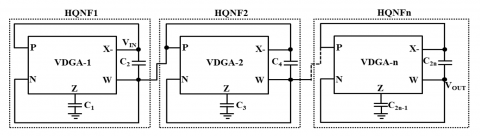
A generalized comb filter, utilizing an n-number of VDGA-based High-Quality Notch Filters (HQNF), as depicted in Figure 10, is implemented in Figure 11. This configuration is capable of blocking n number of undesirable frequencies. The transfer function of the filter circuit can be determined by multiplying the transfer functions of each cascaded VDGA-based HQNF, as given in Eq. (24).
Now, based on (24), the pole frequency (f0n) and the quality factor (Qn) of each HQNF can be expressed as:
${{f}_{0n}}=\frac{1}{2\pi \sqrt{{{L}_{n}}{{C}_{n}}}}=\frac{1}{2\pi }\sqrt{\frac{{{g}_{mAn}}{{g}_{mBn}}}{{{C}_{n}}{{C}_{n-1}}}}$
${{Q}_{n}}=R\sqrt{\frac{{{C}_{n}}}{{{L}_{n}}}}=\frac{1}{{{g}_{mCn}}}\sqrt{\frac{{{C}_{n}}{{C}_{n-1}}}{{{g}_{mAn}}{{g}_{mBn}}}}$ (25)
It is evident from Eq. (25) that the pole frequency, quality factor, and, consequently, the bandwidth of the nth HQNF can be adjusted by varying the transconductances (${{g}_{mAn}}$, ${{g}_{mBn}}$, and ${{g}_{mCn}}$) of their respective VDGA. This adjustment is achieved by varying the bias currents of the respective VDGA while keeping the values of capacitors ${{C}_{n}}~\text{and}~{{C}_{n-1}}$ fixed.
The proposed comb filter, illustrated in Figure 11, has been meticulously designed and simulated with the specific objective of attenuating four frequencies (n = 4) at 50Hz, 150Hz, 250Hz, and 350Hz using the PSPICE simulator software. The rationale behind choosing n = 4 is rooted in the aim to effectively block the PLI at 50Hz and its subsequent three odd harmonics (150Hz, 250Hz, and 350Hz). By accomplishing this, the filter is expected to yield almost clean biomedical signal at its output when processing a PLI-contaminated biomedical signal. Since ECG signals, in particular, and biomedical signals, in general, have low frequencies, removing up to the third harmonic has been proven sufficient to produce biomedical signals almost completely free of PLI. All VDGAs employed in implementing the comb filter for n = 4 have undergone realization using both the 0.18µm CMOS technology process parameters of TSMC and the macro-model of the IC MAX435 separately in the simulation. Subsections 4.1 and 4.2 comprehensively delineate the simulation procedures and present the outcomes obtained through the use of 0.18µm CMOS technology and IC MAX435, respectively.
4.1 Simulation of the proposed comb filter using 0.18µm CMOS technology
First, the proposed comb filter for n = 4 is simulated using 0.18µm CMOS technology. All VDGAs are instantiated using their CMOS schematic, as illustrated in Figure 3. The aspect ratio (W/L) of the MOSFETs in Figure 3 is given in Table 1. The power supplies used for this design are VDD = 900mV and VSS = −900mV. Bias currents of the VDGA are set as IB1 = IB2 = IB3 = IB4 = 480μA and IB5 = IB6 = 224μA. With these bias current values, the transconductance gains of the VDGA are determined as gmA = gmB = 1mS and gmC = 666.67µS in simulation during simulation. The capacitance values for Figure 11 are as follows: (i) C1 = 318.3 nf and C2 = 31.83µf for HQNF1 to set the pole frequency at 50Hz, (ii) C3 = 53.05 nf and C4 = 21.22µf for HQNF2 to set the pole frequency at 150Hz, (iii) C5 = 21.22nf and C6 = 19.09µf for HQNF3 to set the pole frequency at 250Hz, and (iv) C7 = 21.22nf and C8 = 19.09µf for HQNF3 to set the pole frequency at 350Hz.
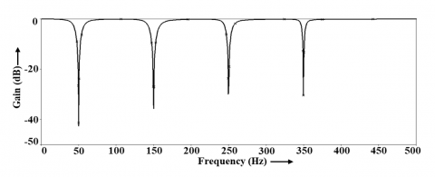
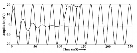
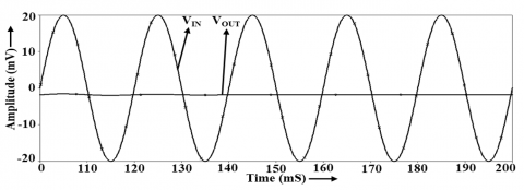
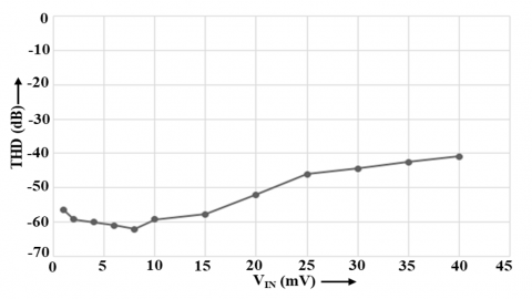
The simulated frequency response, illustrated in Figure 12, affirms the effective attenuation of four pole frequencies (50Hz, 150Hz, 250Hz, and 350Hz), aligning closely with theoretical predictions. The frequency response exhibits sharp notches, as anticipated due to high-quality factors, and the passband regions appear nearly flat, indicating the unaltered transmission of useful biosignals without distortion, except for Power Line Interference (PLI) and its odd harmonics. To assess the filter's performance in the time domain, a 50Hz sinusoidal wave representing PLI is processed, and the simulated input and output waveforms are presented in Figure 13. Following the settling time, the 50Hz input waveform is effectively suppressed, yielding an insignificant waveform at the output. Figure 14 further elucidates the input and output waveforms after the settling time, emphasizing the exceptional ability of the proposed circuit to suppress 50Hz PLI. Lastly, Figure 15 portrays the overall harmonic distortion for a signal at 100Hz, determining the output quality and dynamic range in the passband. The Total Harmonic Distortion (THD) is exceptionally low, measuring up to -62.34dB (peak to peak), indicative of a substantial dynamic range for the proposed filter.
Table 1. Aspect ratios of MOSFET used in Figure 3
|
MOSFETs |
M1A, M2A, M1B, M2B, M1C, M2C |
M3A, M4A, M3B, M4B, M3C, M4C |
|
Types of MOSFET |
p-channel |
n-channel |
|
Width (W) |
16.64µm |
3.6µm |
|
Length (L) |
0.36µm |
0.36µm |
Figure 12. Frequency response of the comb filter using 0.18µm technology
Figure 13. Input and output waveforms at 50Hz
Figure 14. Zoom version of Figure 13
Figure 15. THD of the comb filter implemented in 0.18µm technology
4.2 Simulation of the proposed comb filter using the macro-model of IC MAX435
In this subsection, the simulation of the proposed comb filter involves the use of the macro-model of IC MAX435, a commercially available integrated circuit. The building block of the comb filter, the VDGA, is implemented using the IC MAX435. The realization of VDGA through IC MAX435 is depicted in Figure 4. The resistor values in Figure 4 are set as follows: Rx = 4kΩ, Ry = 4kΩ, Rz = 6kΩ, and Rp1 = Rp2 = Rp3 = 20kΩ. The supply voltages, VDD, and VSS are chosen as +9V and −9V, respectively.
The simulated transconductance gains (gmA=gmB=1mS and gmC = 666.67µS) for the VDGAs are derived using the formula ${{g}_{m}}=\frac{4}{{{R}_{i}}}$ for $i=x,y,and~z$, as provided by the IC MAX435 specifications.
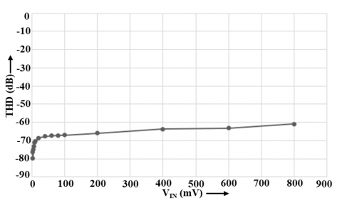
The simulation results include the frequency response and Total Harmonic Distortion (THD) for a 100Hz signal, illustrated in Figure 16 and Figure 17, respectively. The frequency response graph demonstrates the attenuation of specified frequencies, confirming the filter's efficacy. The THD analysis at 100Hz indicates the quality and dynamic range of the passband output signal, with the results presented in Figure 17. These simulation outcomes are crucial for assessing the performance of the proposed comb filter when implemented using the IC MAX435 macro-model.
Figure 16. Frequency response of the comb filter using IC MAX435
Figure 17. THD of the comb filter implemented using IC MAX435
The performances of an ideal circuit are often deviated due to the presence of terminal parasitics in the VDGA, along with voltage and current transfer errors. These parasitics and errors represent practical imperfections that can impact the behavior of the circuit, leading to deviations from the expected ideal performance. Understanding and mitigating these non-idealities are crucial in designing and analyzing circuits to ensure they operate as intended in real-world conditions.
Considering the non-ideal transfer gains and terminal parasitics of the VDGA, the terminal relationship given in Eq. (1) is modified to account for these deviations. The modified terminal relationship is expressed as:
$\left[ \begin{matrix}
\begin{matrix}
{{I}_{P}} \\
{{I}_{N}} \\
\end{matrix} \\
{{I}_{Z}} \\
\begin{matrix}
\begin{matrix}
{{I}_{X}} \\
{{I}_{W}} \\
\end{matrix} \\
{{V}_{W}} \\
\end{matrix} \\
\end{matrix} \right]=\left[ \begin{matrix}
\begin{matrix}
0 & 0 \\
0 & 0 \\
{{\gamma }_{A}}{{g}_{mA}} & -{{\gamma }_{A}}{{g}_{mA}} \\
\end{matrix} & \begin{matrix}
0 & \begin{matrix}
0 & 0 \\
\end{matrix} \\
0 & \begin{matrix}
0 & 0 \\
\end{matrix} \\
0 & \begin{matrix}
0 & 0 \\
\end{matrix} \\
\end{matrix} \\
\begin{matrix}
0 & 0 \\
\end{matrix} & {{\gamma }_{B}}\begin{matrix}
{{g}_{mB}} & \begin{matrix}
0 & 0 \\
\end{matrix} \\
\end{matrix} \\
\begin{matrix}
\begin{matrix}
0 \\
0 \\
\end{matrix} & \begin{matrix}
0 \\
0 \\
\end{matrix} \\
\end{matrix} & \begin{matrix}
\begin{matrix}
-{{\gamma }_{B}}{{g}_{mB}} \\
\frac{{{\gamma }_{B}}}{{{\gamma }_{C}}}\beta \\
\end{matrix} & \begin{matrix}
\begin{matrix}
0 \\
0 \\
\end{matrix} & \begin{matrix}
{{\gamma }_{C}}{{g}_{mC}} \\
0 \\
\end{matrix} \\
\end{matrix} \\
\end{matrix} \\
\end{matrix} \right]\left[ \begin{matrix}
\begin{matrix}
{{V}_{P}} \\
{{V}_{N}} \\
\end{matrix} \\
{{V}_{Z}} \\
\begin{matrix}
{{V}_{X}} \\
{{V}_{W}} \\
\end{matrix} \\
\end{matrix} \right]$ (26)
Here, $\beta =\frac{{{g}_{mB}}}{{{g}_{mC}}}$ and ${{\gamma }_{A}},~{{\gamma }_{B}}~{\text{and}}~{{\gamma }_{C}}$ are transconductance gain errors. Taking these errors into account, the pole frequency (f0) and the quality factor (Q) of the proposed comb filter can be expressed as:
${{f}_{0}}=\frac{1}{2\pi \sqrt{{{L}_{n}}{{C}_{n}}}}=\frac{1}{2\pi }\sqrt{\frac{{{\gamma }_{An}}{{\gamma }_{Bn}}{{g}_{mAn}}{{g}_{mBn}}}{{{C}_{n}}{{C}_{n-1}}}}$ (27)
$Q=R\sqrt{\frac{{{C}_{n}}}{{{L}_{n}}}}=\frac{1}{{{\gamma }_{Cn}}{{g}_{mC}}}\sqrt{\frac{{{C}_{n}}{{C}_{n-1}}}{{{\gamma }_{An}}{{\gamma }_{Bn}}{{g}_{mA}}{{g}_{mB}}}}$ (28)
The sensitivities of f0 and Q with respect to transconductance gain errors and capacitors are derived as follows:
$S_{{{\gamma }_{An}}}^{{{f}_{0}}}=S_{{{\gamma }_{Bn}}}^{{{f}_{0}}}=S_{{{g}_{mAn}}}^{{{f}_{0}}}=S_{{{g}_{mBn}}}^{{{f}_{0}}}={}^{1}/{}_{2}$ (29)
$S_{{{C}_{n}}}^{{{f}_{0}}}=S_{{{C}_{n-1}}}^{{{f}_{0}}}=-{}^{1}/{}_{2}$ (30)
$S_{{{\gamma }_{An}}}^{Q}=S_{{{\gamma }_{Bn}}}^{Q}=S_{{{g}_{mAn}}}^{Q}=S_{{{g}_{mBn}}}^{Q}={}^{1}/{}_{2}$ (31)
$S_{{{C}_{n}}}^{Q}=S_{{{C}_{n-1}}}^{Q}=-{}^{1}/{}_{2}$ (32)
$S_{{{\gamma }_{Cn}}}^{Q}=S_{{{g}_{mCn}}}^{Q}=-1$ (33)
Figure 18. Symbolic representation of a practical VDGA
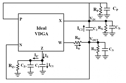
Figure 19. Proposed HQNF, including parasitics
From the derived sensitivities, it is observed that the magnitude of sensitivities is within the acceptable limit of unity. To assess the performance of the real comb filter, the circuit is analyzed considering the terminal parasitics of the VDGA. The practical VDGA, including terminal parasitics, is symbolically represented in Figure 18. Utilizing this representation, the proposed High-Quality Notch Filter (HQNF) can be redrawn, as illustrated in Figure 19.
The transfer function of the practical HQNF, illustrated in Figure 19, is derived as follows:
Applying KCL at node VOUT, the equation ${{I}_{W}}={{I}_{C2}}+{{I}_{N}}$ is obtained and can be expressed using (26) as:
${{g}_{mB}}{{V}_{Z}}-{{g}_{mC}}{{V}_{W}}={{I}_{C2}}+{{I}_{N}}$ (34)
Further, the voltage of the W-terminal, VW, is written using Kirchhoff’s voltage law (KVL) as:
${{V}_{W}}={{V}_{OUT}}+{{I}_{W}}{{R}_{W}}$. (35)
Combining (34) and (35), the following expression is obtained:
${{g}_{mB}}{{V}_{Z}}-{{g}_{mC}}{{V}_{OUT}}={{I}_{C2}}\left( 1+{{R}_{W}}{{g}_{mC}} \right)+{{I}_{N}}\left( 1+{{R}_{W}}{{g}_{mC}} \right)$ (36)
Rearranging (36) with the help of Figure 16, it becomes:
${{g}_{mB}}{{V}_{Z}}-{{g}_{mC}}{{V}_{OUT}}=s{{C}_{2}}\left( {{V}_{OUT}}-{{V}_{IN}} \right)\left( 1+{{R}_{W}}{{g}_{mC}} \right)+{{V}_{OUT}}\frac{\left( s{{C}_{P}}{{R}_{P}}+1 \right)}{{{R}_{P}}}\left( 1+{{R}_{W}}{{g}_{mC}} \right)$. (37)
Again, applying KCL at terminal Z of Figure 19, the equation ${{I}_{Z}}={{I}_{C1}}+{{I}_{Z'}}$ is obtained using (26), and after rearranging, the expression for the voltage at the Z-terminal is derived as:
${{V}_{Z}}=\frac{{{g}_{mA}}\left( {{V}_{IN}}-{{V}_{OUT}} \right)}{s{{C}_{1}}+\frac{\left( s{{C}_{Z}}{{R}_{Z}}+1 \right)}{{{R}_{Z}}}}$ (38)
From Eqs. (37) and (38), the combined expression is derived:
$\frac{{{g}_{mA}}{{g}_{mB}}\left( {{V}_{IN}}-{{V}_{OUT}} \right)}{s{{C}_{1}}+\frac{\left( s{{C}_{Z}}{{R}_{Z}}+1 \right)}{{{R}_{Z}}}}-{{g}_{mC}}{{V}_{OUT}}=s{{C}_{2}}\left( {{V}_{OUT}}-{{V}_{IN}} \right)\left( 1+{{R}_{W}}{{g}_{mC}} \right)+{{V}_{OUT}}\frac{\left( s{{C}_{P}}{{R}_{P}}+1 \right)}{{{R}_{P}}}\left( 1+{{R}_{W}}{{g}_{mC}} \right)$ (39)
Rearranging (39), we get the following transfer function,
$H\left( s \right)=\frac{{{V}_{OUT}}\left( s \right)}{{{V}_{IN}}\left( s \right)}=\frac{{{s}^{2}}\left( 1+{{R}_{W}}{{g}_{mC}} \right)+\frac{s\left( s{{C}_{Z}}{{R}_{Z}}+1 \right)\left( 1+{{R}_{W}}{{g}_{mC}} \right)}{{{C}_{1}}{{R}_{Z}}}+\frac{{{g}_{mA}}{{g}_{mB}}}{{{C}_{1}}{{C}_{2}}}}{s{{C}_{1}}\left( 1+{{R}_{W}}{{g}_{mC}} \right)\left[ s{{C}_{1}}+\frac{\left( s{{C}_{Z}}{{R}_{Z}}+1 \right)}{{{R}_{Z}}} \right]+{{g}_{mC}}\left[ s{{C}_{1}}+\frac{\left( s{{C}_{Z}}{{R}_{Z}}+1 \right)}{{{R}_{Z}}} \right]+\left[ s{{C}_{1}}+\frac{\left( s{{C}_{Z}}{{R}_{Z}}+1 \right)}{{{R}_{Z}}} \right]\left[ \frac{\left( s{{C}_{P}}{{R}_{P}}+1 \right)}{{{R}_{P}}} \right]\left( 1+{{R}_{W}}{{g}_{mC}} \right)+{{g}_{mA}}{{g}_{mB}}}$ (40)
In summary, the transfer function derived in (40) reveals that the proposed filter may experience some impact due to the parasitics of the real VDGA. However, under conditions of low terminal parasitic capacitances, low RW values, and high RP and RZ values, Eq. (40) simplifies, yielding the same transfer function as in Eq. (21). This analysis concludes that the proposed filter's non-ideal effects can be effectively suppressed within satisfactory limits by carefully selecting an appropriate architecture for the VDGA.
The performance of the proposed comb filter utilizing the VDGA is meticulously compared in Table 2 with existing circuits found in the literature, considering various aspects such as application, technology, active block, number of active blocks, number of passive components, voltage supply, rejection frequency, notch depth, and THD. Table 2 clearly illustrates that the circuits documented in studies [12, 13, 15, 18, 19, 23-31], and Kumngern et al. [33] are primarily designed for notching a single frequency only. Through this comparative analysis, it is evident that the proposed structure stands out as highly advantageous, requiring fewer active blocks and passive components when compared to designs presented in studies [14, 16, 17, 21], all while achieving notching for the same number of undesirable frequencies (n=4).
A key advantage of the proposed filter lies in its compact design, occupying less chip area and eliminating the need for resistors in its configuration. The depth of the notch is a crucial parameter influencing the filter's ability to attenuate frequencies within the notch. The proposed comb filter achieves a notable -42.9dB notch depth, effectively eliminating undesired frequencies. It is acknowledged that an excessively deep notch may introduce complications like phase distortion or group delay; thus, the filter design strikes a balance between achieving the desired notch depth and preserving other essential performance characteristics.
The proposed comb filter excels in terms of THD, an important parameter in filter evaluation due to its potential introduction of distortion in the passband, particularly in the presence of harmonics. The simulation results demonstrate that the proposed filter attains an exceptional -83dB THD, signifying superior performance compared to existing filter structures. This observation underscores the filter's effectiveness in passing signals through the passband region without introducing distortion, contributing to its overall high-quality performance.
Table 2. Performance comparison of various implementations of the comb filter
|
Ref. |
Application |
Technology Used |
Active Block |
No. of Active Block used |
No. of Passive Components Used |
Voltage Supply |
Rejection Frequency |
Notch Depth (dB) |
THD (dB) |
|
[12] |
ECG |
BJT |
Op-amp |
10 |
Resistor-27 Capacitor-03 |
-- |
60 |
-60 |
-- |
|
[13] |
ECG |
CMOS 0.18µm |
OP-amp |
3 |
Resistor-03 Capacitor-06 |
1.8V |
50 |
-55.4 |
-- |
|
[14] |
ECG |
BJT |
Op-amp |
5 |
Resistor-18 Capacitor-08 |
-- |
60, 180, 300, 420 |
-- |
-- |
|
[15] |
ECG |
CMOS 0.35µm |
CCII |
4 |
Resistor-08
|
1.5V |
50 |
-- |
-- |
|
[16] |
ECG |
CMOS 0.5µm |
OTA |
10 |
Capacitor-08 |
$\pm 5\text{V}$ |
60, 180, 300, 420 |
-- |
-40 |
|
[17] |
EEG, ECG, EMG |
CMOS 0.18µm |
CCII+ |
7 |
Resistor-19
|
$\pm .4\text{V}$ |
60, 180, 300, 420 |
-61 to-64 |
-48 |
|
[17] |
EEG, ECG, EMG |
BJT |
ADA844 |
7 |
Capacitor-08 |
/$\pm 5\text{V}$ |
60, 180, 300, 420 |
-37 to-50 |
-43 |
|
[18] |
EEG |
CMOS 0.35µm |
OTA |
6 |
Capacitor-07 |
$\pm 1.5\text{V}$ |
50 |
-66 |
-50 |
|
[19] |
EEG, ECG, EMG |
CMOS 0.18µm |
OTA |
11 |
Capacitor-05 |
$1.5\text{V}$ |
60 |
-60 |
-60 |
|
[20] |
EEG, ECG, EMG |
CMOS 0.18µm |
OP-amp |
3 |
Resistor-06 Capacitor-03 |
1.5V |
40-80 |
-43 |
-70 |
|
[21] |
EEG, ECG, EMG |
BJT |
ADA844 |
8 |
Resistor-11, Capacitor-08 |
$\pm 5\text{V}$ |
50, 150, 250, 350 |
-31 to-36 |
-65 to-75 |
|
[21] |
EEG, ECG, EMG |
DTMOS 0.18µm |
CCII+ |
8 |
Resistor-11, Capacitor-08 |
$\pm 0.2\text{V}$ |
50, 150, 250, 350 |
-35 to-58 |
-40 to-58 |
|
[22] |
EEG |
CMOS 0.25µm |
DPOTA |
6 |
Capacitor-07 |
$\pm 0.8\text{V}$ |
50, 150 |
-59, -40 |
-- |
|
[23] |
ECG |
CMOS 0.18µm |
OTA |
|
Capacitor-08 |
1,8V |
50 |
-- |
-40 |
|
[24] |
ECG |
CMOS 0.18µm |
MOFD-OTA |
6 |
Capacitor-06 |
1V |
250 |
-- |
-- |
|
[25] |
ECG, EMG |
BJT |
Op-amp |
2 |
Resistor-06, Capacitor-04 |
15V |
60 |
-60.28 |
-- |
|
[26] |
ECG |
CMOS 65nm |
OTA |
4 |
Capacitor-02 |
$\pm 0.5\text{V}$ |
60 |
-11 |
--- |
|
[27] |
EEG, ECG, EMG |
CMOS 90nm |
OTA |
8 |
Capacitor-08 |
$\pm 0.6\text{V}$ |
50 |
-44 |
-51 |
|
[28] |
ECG |
CMOS 0.18µm |
OTA |
3 |
Resistor-03, Capacitor-04 |
1.8V |
50 |
--- |
-76 |
|
[29] |
ECG |
CMOS 0.25µm |
MO-OTA |
9 |
Capacitor-06 |
$\pm 0.75\text{V}$ |
50 |
-40 |
--- |
|
[30] |
--- |
CMOS 0.18μm |
VD-DIBA |
2 |
Resistor-02, Capacitor-02 |
± 0.9V |
95.50kHz |
--- |
38.75 |
|
[31] |
--- |
CMOS 0.13µm |
DDTA |
3 |
Resistor-01, Capacitor-02 |
0.5V |
231 |
--- |
--- |
|
[32] |
EEG |
DTMOS 0.18µm |
MIMO OTA |
6 |
Capacitor-09 |
0.5V |
50&150 |
−37.2&−47.4 |
49.7 |
|
[33] |
ECG |
CMOS 0.18µm |
MI-DDTA |
3 |
Resistor-01 Capacitor-02 |
±0.5V |
1.03kHz |
--- |
1.14@250mVpp |
|
Proposed work |
EEG, ECG, EMG |
0.18µm CMOS |
VDGA |
4 |
Capacitor-08 |
± 0.9V |
50, 150, 250, 350 |
-42.9 |
-83. |
A VDGA-based analog comb filter circuit has been successfully designed and implemented, showcasing the versatility and adaptability of the VDGA as a primary active element. The simplicity of the circuit lies in the utilization of one VDGA as the active component, complemented by the integration of two capacitors as passive elements strategically employed for notching a single undesired frequency. The scalability of the design is demonstrated by extending the concept to notch n undesired frequencies, achieved through the deployment of n VDGA and 2n capacitors. The electronic tunability of the comb filter's characteristics, facilitated by adjusting VDGA bias currents, adds a layer of flexibility to the design.
To validate the theoretical predictions and assess the circuit's real-world performance, comprehensive simulations were conducted using PSPICE. The filter's efficacy was tested against power line frequency (50Hz) and its three odd harmonics (150Hz, 250Hz, and 350Hz), considering both the 0.18µm CMOS technology and the commercially available IC MAX435 macro-model. The study delves into non-ideal considerations and component sensitivity analysis, providing a holistic view of the filter's behavior in practical scenarios.
In a comparative analysis with existing architectures, the proposed comb filter stands out for its effectiveness and improvements, substantiating its potential as a valuable contribution to the field. The proposed notch filter, tailored for biomedical signal detection applications such as EEG, EMG, and ECG, showcases promising outcomes, paving the way for enhanced signal processing in these critical domains.
While the current work demonstrates significant advancements, there remains ample room for further exploration and improvement in filter circuit performance, particularly regarding area and power efficiency. Future research avenues could explore incorporating additional features to broaden the scope of applications. Experimentation with alternative variants of VDGA available in the literature may yield insights into further enhancing filter performance parameters. The potential reduction in power dissipation and chip area could be explored by designing a VDGA block using more advanced technologies, such as 130nm/90nm/45nm. Additionally, exploring unconventional materials like Carbon Nano Tubes (CNT) or FinFET (Fin field effect transistor) devices in lieu of traditional MOS transistors could significantly improve power efficiency, chip area, and overall filter performance. Continuous and dynamic research efforts will be essential to unlock new possibilities and propel technological advancements in the realm of analog comb filter design.
[1] Huhta, J.C., Webster, J.G. (1973). 60-Hz interference in electrocardiography. IEEE Transactions on Biomedical Engineering, (2): 91-101. https://doi.org/10.1109/TBME.1973.324169
[2] Mantri, S., Patil, D., Agrawal, P., Wadhai, V. (2015). Non invasive EEG signal processing framework for real time depression analysis. In 2015 SAI intelligent systems conference (IntelliSys), London, UK, pp. 518-521. https://doi.org/10.1109/IntelliSys.2015.7361188
[3] Vigário, R., Sarela, J., Jousmiki, V., Hamalainen, M., Oja, E. (2000). Independent component approach to the analysis of EEG and MEG recordings. IEEE Transactions on Biomedical Engineering, 47(5): 589-593. https://doi.org/10.1109/10.841330
[4] Singh, B., Singh, P., Budhiraja, S. (2015) Various approaches to minimise noises in ECG signal: A survey. Fifth International Conference on Advanced Computing & Communication Technologies, Haryana, India, 131-137. https://doi.org/10.1109/ACCT.2015.87
[5] Ziarani, A.K., Konrad, A. (2002). A nonlinear adaptive method of elimination of power line interference in ECG signals. IEEE Transactions on Biomedical Engineering, 49(6): 540-547. https://doi.org/10.1109/TBME.2002.1001968
[6] Oster, J., Behar, J., Sayadi, O., Nemati, S., Johnson, A.E., Clifford, G.D. (2015). Semisupervised ECG ventricular beat classification with novelty detection based on switching Kalman filters. IEEE Transactions on Biomedical Engineering, 62(9): 2125-2134. https://doi.org/10.1109/TBME.2015.2402236
[7] Li, Q., Clifford, G.D. (2012). Signal quality and data fusion for false alarm reduction in the intensive care unit. Journal of Electrocardiology, 45(6): 596-603. https://doi.org/10.1016/j.jelectrocard.2012.07.015
[8] Falk, T.H., Maier, M. (2014). MS-QI: A modulation spectrum-based ECG quality index for telehealth applications. IEEE Transactions on Biomedical Engineering, 63(8): 1613-1622. https://doi.org/10.1109/TBME.2014.2355135
[9] Orphanidou, C., Estève, D., Bonnet, S. (2015). Signal quality indices for the electrocardiogram and photoplethysmogram: Derivation and applications to wireless monitoring. IEEE Journal of Biomedical and Health Informatics, 19(3): 832-840.
[10] Castro, D., Félix, P., Presedo, J. (2014). A method for context-based adaptive QRS clustering in real time. IEEE Journal of Biomedical and Health Informatics, 19(5): 1660-1671. https://doi.org/10.1109/JBHI.2014.2361659
[11] Takalokastari, T., Alasaarela, E., Kinnunen, M., Jämsä, T. (2013). Quality of the wireless electrocardiogram signal during physical exercise in different age groups. IEEE Journal of Biomedical and Health Informatics, 18(3): 1058-1064. https://doi.org/10.1109/JBHI.2013.2282934
[12] Casper, B.K., Comer, D.J., Comer, D.T. (1999). An integrable 60-Hz notch filter. IEEE Transactions on Circuits and Systems II: Analog and Digital Signal Processing, 46(1): 74-77. https://doi.org/10.1109/82.749101
[13] Ferri, G., Stornelli, V., Di Simone, A. (2011). A CCII-based high impedance input stage for biomedical applications. Journal of Circuits, Systems, and Computers, 20(08): 1441-1447. https://doi.org/10.1142/S021812661100802X
[14] Tsai, C.T., Chan, H.L., Tseng, C.C., Wu, C.P. (1994). Harmonic interference elimination by an active comb filter [ECG application]. In Proceedings of 16th Annual International Conference of the IEEE Engineering in Medicine and Biology Society, Baltimore, MD, USA, 2: 964-965. https://doi.org/10.1109/IEMBS.1994.415235
[15] Li, H., Zhang, J., Wang, L. (2011). A fully integrated continuous-time 50-Hz notch filter with center frequency tunability. In 2011 Annual International Conference of the IEEE Engineering in Medicine and Biology Society, Boston, MA, USA, pp. 3558-3562. https://doi.org/10.1109/IEMBS.2011.6090593
[16] Ranjan, R.K., Yalla, S.P., Sorya, S., Paul, S.K. (2014). Active comb filter using operational transconductance amplifier. Active and Passive Electronic Components, 2014. https://doi.org/10.1155/2014/587932
[17] Ranjan, R.K., Choubey, C.K., Nagar, B.C., Paul, S.K. (2016). Comb filter for elimination of unwanted power line interference in biomedical signal. Journal of Circuits, Systems and Computers, 25(06): 1650052. https://doi.org/10.1142/S0218126616500523
[18] Qian, X., Xu, Y.P., Li, X. (2005). A CMOS continuous-time low-pass notch filter for EEG systems. Analog Integrated Circuits and Signal Processing, 44: 231-238. https://doi.org/10.1007/s10470-005-3007-x
[19] Lee, S.Y., Cheng, C.J. (2009). Systematic design and modeling of a OTA-C filter for portable ECG detection. IEEE Transactions on Biomedical Circuits and Systems, 3(1): 53-64. https://doi.org/10.1109/TBCAS.2008.2007423
[20] Alzaher, H.A., Tasadduq, N., Mahnashi, Y. (2013). A highly linear fully integrated powerline filter for biopotential acquisition systems. IEEE Transactions on Biomedical Circuits and Systems, 7(5): 703-712. https://doi.org/10.1109/TBCAS.2013.2245506
[21] Paul, S.K., Choubey, C.K., Tiwari, G. (2018). Low power analog comb filter for biomedical applications. Analog Integrated Circuits and Signal Processing, 97: 371-386. https://doi.org/10.1007/s10470-018-1329-8
[22] Alhammadi, A.A., Mahmoud, S.A. (2016). Fully differential fifth-order dual-notch powerline interference filter oriented to EEG detection system with low pass feature. Microelectronics Journal, 56: 122-133. https://doi.org/10.1016/j.mejo.2016.08.014
[23] Machha Krishna, J.R., Laxminidhi, T. (2019). Widely tunable low‐pass gm-C filter for biomedical applications. IET Circuits, Devices & Systems, 13(2): 239-244. https://doi.org/10.1049/iet-cds.2018.5002
[24] Lee, S.Y., Wang, C.P., Chu, Y.S. (2019) Low-Voltage OTA-C filter with an Area- and Power-Efficient OTA for biosignal sensor applications, IEEE Transactions on Biomedical Circuits and Systems, 13(1): 56-67.
[25] Panja, A., Bhattacharya, A., Banerjee, T.P. (2020) Design and analysis of notch depth for T-notch filter, National Conference on Emerging Trends on Sustainable Technology and Engineering Applications (NCETSTEA), Durgapur, India, 1-4. https://doi.org/10.1109/NCETSTEA48365.2020.9119943
[26] Arce-Zavala, J., Vazquez, A.M., Padilla-Cantoya, I., Plascencia, F. (2020). A Gm-C notch filter implemented with g m Over I D technique for biosignal acquisition systems. In 2020 17th International Conference on Electrical Engineering, Computing Science and Automatic Control (CCE), Mexico City, Mexico, pp. 1-6. IEEE. https://doi.org/10.1109/CCE50788.2020.9299196
[27] Diab, M.S., Mahmoud, S.A. (2020). 14: 5nW; 30 dB analog front-end in 90-nm technology for biopotential signal detection. In 2020 43rd International Conference on Telecommunications and Signal Processing (TSP) Milan, Italy, 681-684. https://doi.org/10.1109/TSP49548.2020.9163572
[28] Zhang, J., Chan, S.C., Li, H., Zhang, N., Wang, L. (2020) An area-efficient and highly linear reconfigurable continuous-time filter for biomedical sensor applications. Sensors (Basel), 20(7): 2065. https://doi.org/10.3390/s20072065
[29] Srisamranrungrueang, S., Wongprommoon, N., Prommee, P. (2021). High-order chebyshev notch filter based on MO-OTA and its application in Biosensor. In 2021 18th International Conference on Electrical Engineering/Electronics, Computer, Telecommunications and Information Technology (ECTI-CON), Chiang Mai, Thailand, 696-699. https://doi.org/10.1109/ECTI-CON51831.2021.9454922
[30] Jaikla, W., Siripongdee, S., Khateb, F., Sotner, R., Silapan, P., Suwanjan, P., Chaichana, A. (2021). Synthesis of biquad filters using two VD-DIBAs with independent control of quality factor and natural frequency. AEU-International Journal of Electronics and Communications, 132: 153601. https://doi.org/10.1016/j.aeue.2020.153601
[31] Kumngern, M., Suksaibul, P., Khateb, F., Kulej, T. (2022). Electronically tunable universal filter and quadrature oscillator using low-voltage differential difference transconductance amplifiers. IEEE Access, 10: 68965-68980. https://doi.org/10.1109/ACCESS.2022.3186435
[32] Kumngern, M., Khateb, F., Kulej, T., Arbet, D., Akbari, M. (2022). Fully differential fifth-order dual-notch low-pass filter for portable EEG system. AEU-International Journal of Electronics and Communications, 146: 154122. https://doi.org/10.1016/j.aeue.2022.154122
[33] Kumngern, M., Khateb, F., Kulej, T. (2023). Shadow filters using multiple-input differential difference transconductance amplifiers. Sensors, 23(3): 1526. https://doi.org/10.3390/s23031526
[34] Hirunporm, J., Siripruchyanun, M. (2020). An independently/electronically controllable Schmitt trigger using only single VDGA. In 2020 17th International Conference on Electrical Engineering/Electronics, Computer, Telecommunications and Information Technology (ECTI-CON), Phuket, Thailand, 118-121. https://doi.org/10.1109/ECTI-CON49241.2020.9158058
[35] Satansup, J., Tangsrirat, W. (2015). Single VDGA-based first-order allpass filter with electronically controllable passband gain. In 2015 7th International Conference on Information Technology and Electrical Engineering (ICITEE), Chiang Mai, Thailand, 106-109. https://doi.org/10.1109/ICITEED.2015.7408922
[36] Channumsin, O., Tangsrirat, W. (2020). Compact dual-mode SITO universal filter and quadrature oscillator with only single VDGA. In 2020 17th International Conference on Electrical Engineering/Electronics, Computer, Telecommunications and Information Technology (ECTI-CON), Phuket, Thailand, 181-184. https://doi.org/10.1109/ECTI-CON49241.2020.9158232
[37] Siripruchyanun, M., Theppota, B. (2022). Single VDGA-based first-order all-pass filter using grounded capacitor. In 2022 International Symposium on Intelligent Signal Processing and Communication Systems (ISPACS), Penang, Malaysia, 1-4. https://doi.org/10.1109/ISPACS57703.2022.10082847
[38] Satansup, J., Tangsrirat, W. (2013) CMOS realization of voltage differencing gain amplifier (VDGA) and its application to biquad filter. Industrial Journal Engineers Materials Science, 20(6): 457-464.
[39] Choubey, C.K., Paul, S.K. (2023). Systematic realisation of inductorless and resistorless Chua’s chaotic oscillator using VDGA. International Journal of Electronics, 110(6): 1006-1027. https://doi.org/10.1080/00207217.2022.2068200
[40] Arbel, A.F., Goldminz, L. (1992). Output stage for current-mode feedback amplifiers, theory and applications. Analog Integrated Circuits and Signal Processing, 2: 243-255. https://doi.org/10.1007/BF00276637