Xinying Zhang![]() | Xixi Han*
| Xixi Han*![]() | Chuannan Fu
| Chuannan Fu![]()
© 2023 IIETA. This article is published by IIETA and is licensed under the CC BY 4.0 license (http://creativecommons.org/licenses/by/4.0/).
OPEN ACCESS
As a core component of electronic products in industrial production, the printed circuit board (PCB) is highly integrated, and carries various electronic components and complex wire layout. Although the PCB has a small size, its defect detection directly affects the quality of circuit board, which is of great significance. This research aimed to study PCB defect detection based on machine vision technology, because the product quality inspection requirements have been continuously increasing in industrial modernization. Whether the object region segmentation algorithms are fast, effective, and accurate directly affects the effects and efficiency of subsequent machine vision defect detection, because object region segmentation is a key step in PCB defect detection. Three types of object region segmentation algorithms, namely, color space threshold segmentation, morphological edge detection segmentation, and K-means clustering segmentation, were studied, and their advantages and disadvantages were analyzed in detail. A suitable algorithm was selected for detection object through experiments, which laid the foundation for better algorithm improvement and segmented object regions quickly and accurately in the defect detection process.
object region segmentation, PCB, color space threshold segmentation algorithm, morphological edge detection segmentation algorithm, K-means clustering segmentation algorithm
Due to industrial automation and the miniaturization development trend of electronic products, the production manufacturing process of PCBs has becoming increasingly complex, and the PCB has been increasingly well-made and tends to be lighter, thinner and smaller, which also puts forward higher requirements for product quality inspection. Compared with traditional manual detection methods, the defect detection methods based on machine vision technology and image processing technology have several advantages, such as non-contact, highly efficient and accurate. Therefore, the detection methods combined with artificial intelligence, machine vision, and image processing have become the industrial detection trend [1-3].
The defect information of a PCB image is reflected by changes in the small-scale wiring layer region, including changes in edge contour and color. The wiring layer region should be accurately segmented from the image in order to reduce the amount of calculation in the defect detection algorithm. The accuracy of object region segmentation is an important prerequisite for PCB defect detection. At present, most color image segmentation algorithms are obtained by combining the grayscale image segmentation algorithm with the appropriate color space. It is necessary to choose the appropriate method in practice, based on the specific application environment [4-6].
In the study [7], a series of image processing algorithms were used for threshold segmentation and feature extraction of solder joint region in the image, which realized defect detection. As for the low-efficiency traditional sorting of PCB defects in the semiconductor industry, a supervised learning-based model was applied to sort PCB defect detection by Pham et al. [8]. The K-means clustering segmentation algorithm was used by Niu et al. [9] to detect the bare PCB, which aimed to improve the detection accuracy and speed. As for the characteristics of fuzziness and noise in PCB optoelectronic images, a circle detection method of the images was proposed by Qiao et al. [10, 11] based on the improved Hough transform. The basic principle of circle detection based on the traditional Hough transform algorithm was first discussed, and the shortcomings were pointed out. Then the basic principle of the circle detection method based on the improved Hough transform was analyzed in detail. The adopted image processing algorithm obtained the best edge information and had short calculation time. A PCB automatic detection method was proposed by Hassanin et al. [12-15], which accurately determined the fault location and identified the fault type. Several digital image processing technologies were used, including registration, filtering, foreground segmentation, mathematical morphology operation, subtraction, feature extraction and component matching. PCB solder joints were detected by Jiang et al. [16] based on the automatic threshold image segmentation algorithm and the mathematical morphology image processing algorithm.
In order to meet the real-time requirements of defect detection, the segmentation algorithm should be accurate and fast and minimize the complexity [17-19]. After analyzing three types of image segmentation algorithms, namely, color space threshold segmentation, morphological edge detection segmentation, and K-means clustering segmentation, these algorithms were used to segment PCB images. The optimal algorithm was selected through experimental comparison, which reduced the amount of calculation, improved detection efficiency, and retained the color information of the detected images.
2.1 Color space threshold segmentation algorithm
Histogram threshold segmentation algorithm is the most common segmentation algorithm. Significant gray difference exists between the object and background regions, and corresponds to different peaks in the gray distribution histogram, which is the theoretical basis of the algorithm. The threshold was selected between the peaks to segment the image into object and background regions. Although this method is intuitive and segments images with strong changes in brightness and darkness very well, it is sensitive to non-uniform color in the same region.
In the uniform color space, the color difference among all PCB image regions has obvious separability, as shown in Figure 1. Therefore, the threshold was set in the CIE L*a*b* space and the pixels were classified in order to realize the object segmentation.
Figure 1. Distribution of PCB image pixels in the CIE L*a*b* space
After calculating the components of L*, a* and b*, corresponding to all pixels in the filtered image, they were mapped to the CIE L*a*b* space, as shown in the following formula.
$RGB\left\{ f\left( x,y \right) \right\}\Rightarrow \left\{ \left( {{L}^{*}},{{a}^{*}},{{b}^{*}} \right) \right\}$ (1)
The correspondence between the pixel $f(x, y)$ and the point (L*a*b*) in the CIE L*a*b* space was established. Although the pixels in the same region were far apart in the image, they concentrated in the CIE L*a*b* space. However, due to color difference, the pixels in different regions were far apart in the space. After setting the threshold range of three dimensions $U_{L^*}, U_{a^*}$ and $U_{b^*}$, the spatial point set was divided into two categories, i.e. pixels in the object and background regions. The discriminant was as follows:
$T\left\{ \xi \right\}=\left\{ \begin{matrix} \begin{matrix} A & {{\xi }_{{{L}^{*}}}}\in {{U}_{{{L}^{*}}}},{{\xi }_{{{a}^{*}}}}\in {{U}_{{{a}^{*}}}},{{\xi }_{{{b}^{*}}}}\in {{U}_{{{b}^{*}}}} \\\end{matrix} \\ \begin{matrix} B\text{ } & other \\\end{matrix} \\\end{matrix} \right.$ (2)
The points, with all three spatial components within the threshold range, were the object points, and the corresponding pixels were the object region pixels and labeled as category A points. The remaining points were background points, and the corresponding pixels were labeled as category B points.
The threshold range should be determined based on the object region pixel distribution of the PCB image in the CIE L*a*b* space. After obtaining the mean point coordinates of spatial distribution $\left(\overline{L^*}, \overline{a^*}, \overline{b^*}\right)$ and the distribution variances in all dimensions $\sigma_{L^*}, \sigma_{a^*}$ and $\sigma_{b^*}$, the threshold range was determined according to the $\sigma$ principle, as shown in Formula (5). For image detection of PCBs in the same batch, the obtained threshold range was used as a fixed value.
$\left\{ \begin{matrix} \overline{{{L}^{*}}}=\frac{\sum\limits_{i=1}^{n}{{{L}_{i}}^{*}}}{n} \\ \overline{{{a}^{*}}}=\frac{\sum\limits_{i=1}^{n}{{{a}_{i}}^{*}}}{n} \\ \overline{{{b}^{*}}}=\frac{\sum\limits_{i=1}^{n}{{{b}_{i}}^{*}}}{n} \\\end{matrix} \right.$ (3)
$\left\{ \begin{matrix} {{\sigma }_{{{L}^{*}}}}=\sqrt{\frac{\sum\limits_{i=1}^{n}{{{\left( {{L}_{i}}^{*}-\overline{{{L}^{*}}} \right)}^{2}}}}{n-1}} \\ {{\sigma }_{{{a}^{*}}}}=\sqrt{\frac{\sum\limits_{i=1}^{n}{{{\left( {{a}_{i}}^{*}-\overline{{{a}^{*}}} \right)}^{2}}}}{n-1}} \\ {{\sigma }_{{{b}^{*}}}}=\sqrt{\frac{\sum\limits_{i=1}^{n}{{{\left( {{b}_{i}}^{*}-\overline{{{b}^{*}}} \right)}^{2}}}}{n-1}} \\\end{matrix} \right.$ (4)
$\left\{ \begin{matrix} {{U}_{{{L}^{*}}}}=\left[ \overline{{{L}^{*}}}-6{{\sigma }_{{{L}^{*}}}},\overline{{{L}^{*}}}+6{{\sigma }_{{{L}^{*}}}} \right] \\ {{U}_{{{a}^{*}}}}=\left[ \overline{{{a}^{*}}}-6{{\sigma }_{{{a}^{*}}}},\overline{{{a}^{*}}}+6{{\sigma }_{{{a}^{*}}}} \right] \\ {{U}_{{{b}^{*}}}}=\left[ \overline{{{b}^{*}}}-6{{\sigma }_{{{b}^{*}}}},\overline{{{b}^{*}}}+6{{\sigma }_{{{b}^{*}}}} \right] \\\end{matrix} \right.$ (5)
To enhance the separability of pixels among regions, the image linear contrast was enhanced simply in the RGB (red, green and blue) space before segmentation, as shown in Formula (6).
${{f}_{E}}\left( \xi \right)=\left\{ \begin{matrix} \begin{matrix} 0 & \alpha f\left( \xi \right)+\beta \prec 0 \\\end{matrix} \\ \begin{matrix} \alpha f\left( \xi \right)+\beta & 0\le \alpha f\left( \xi \right)+\beta \le 255 \\\end{matrix} \\ \begin{matrix} 255 & \alpha f\left( \xi \right)+\beta \succ 255 \\\end{matrix} \\\end{matrix} \right.$ (6)
where, $f(\xi)$ is the R, G, and B components of the pixel $\xi$. The amplification coefficient α and the translation coefficient β were determined through experiment.
The color space threshold segmentation algorithm had a simple principle, a small amount of calculation, and fast execution speed. However, the threshold range process parameters were selected based on a large number of experiments. At the same time, the threshold selection lacked the adaptive ability and the algorithm had poor robustness.
2.2 Morphological edge detection segmentation algorithm
Edge detection of a grayscale image is generally realized by calculating the first or second derivative of the image. However, the image gradient is generally calculated in practical operation, by considering that the image does not meet the continuous derivable condition.
In the edge detection algorithm, the derivative or gradient information of the image is used to judge the edge, which leads to a contradiction between noise resistance and detection precision. In addition, the algorithm is highly complex.
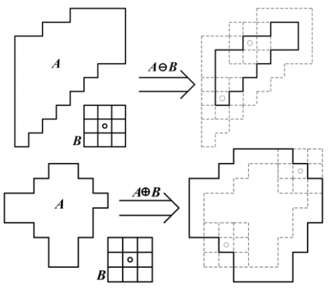
The two basic operations of morphology are corrosion and expansion, which are the basis of many morphological treatments. The mathematical expressions of corrosion and expansion operations are shown in Formulas (7) and (8).
$A\Theta B=\left\{ \forall b\in B,\exists a\in A:x=a-b \right\}=\left\{ x|{{\left( B \right)}_{x}}\subseteq A \right\}$ (7)
$A\oplus B=\left\{ \exists a\in A,b\in B:x=a+b \right\}=\left\{ x|\left[ {{\left( \overset{\wedge }{\mathop{B}}\, \right)}_{x}}\bigcap A \right]\ne \varnothing \right\}$ (8)
where, A is the pixel set, B is the structuring element, $\widehat{B}$ is the complementary set of B, and $\varnothing$ is an empty set. Corrosion can be understood as the set of x that remains in A after B has successively translated x on A. Expansion can be understood as the set of all translations x of B on A, which satisfies the condition that the intersection between $\widehat{B}$ and A is not empty. Figure 2 is a schematic diagram of corrosion and expansion operations, with the 3×3 rectangle as the structuring element B.
Figure 2. Principle of corrosion and expansion operations
Expansion expands the region contour in the image, while corrosion reduces the region contour, leading to the following conclusion.
$A\Theta B\le A\le A\oplus B$ (9)
The difference between the two was the edge contour of the image, which was defined as the gradient operator in morphology and was described below.
$Gra{{d}_{M}}=A\oplus B-A\Theta B$ (10)
Brightness component map of the image in the CIE L*a*b* space was first separated, and the image edge contour was obtained according to Formula (10), which segmented the object region. The morphological edge detection obtained clear edge, because differentiation and others were not needed to be calculated. The noise interference on the results was eliminated by changing the size of the structuring element. At the same time, the edge obtained by subtraction operation retained edge details very well. Therefore, the edge detection effects of PCB images were significantly better than that of the gradient operation-based edge detection algorithm. However, the edge detected by this method was greatly influenced by the shape and size of the structuring element, which may lead to "over-processed" defect edge details during corrosion and expansion operations due to the structuring element selection, resulting in a certain degree of information distortion and affecting the defect feature extraction.
2.3 K-means clustering segmentation algorithm
The color space threshold segmentation algorithm needs to be supported by prior knowledge, while the shape and size of the structuring element needs to be set according to the actual situation in the morphological edge segmentation algorithm. Due to human intervention, the segmentation results of these methods were influenced by subjective factors. However, the clustering means data self-organizing into several meaningful clusters using certain similarity measure, and is an unsupervised learning method. The entire process is completely driven by the data itself, without the information involvement of known clusters.
The K-means clustering algorithm is a partition-based clustering method, which aims to find K cluster centers c1, c2, …, ck, and enable the quadratic sum of the distance between each data point xi and its nearest cluster center cv to be minimized [15].
PCB image pixels have good separability in the CIE L*a*b* space, and the region types of the PCB image are definite, including wiring layer, solder mask, silk screen layer, pad, plated through hole and so on. The selection of K cluster centers is clear, when the PCB image is segmented using the K-means clustering algorithm.
Based on the above considerations, the K-means clustering algorithm was used to segment the PCB image. The specific steps were as follows:
1. After all pixels of the PCB image were mapped to the CIE L*a*b* space to form the data point set $P=\left\{x_1, x_2, \cdots x_n\right\}$, the index relationships of coordinate positions between the data points and corresponding pixels in the image were established;
2. According to the situation in Figure 1, three initial cluster centers were selected, and labeled as c1, c2 and c3;
3. After calculating the distance between each data point xi and each cluster center, the data point was categorized into the cluster Cv of the nearest cluster center. The distance was calculated according to Formula (11), and the classification of clusters met the following conditions:
$\left\| \left. f\left( x,y \right)-f\left( m,n \right) \right\| \right.=\sqrt{{{\left( {{L}^{*}}_{x,y}-{{L}^{*}}_{m,n} \right)}^{2}}+{{\left( {{a}^{*}}_{x,y}-{{a}^{*}}_{m,n} \right)}^{2}}+{{\left( {{b}^{*}}_{x,y}-{{b}^{*}}_{m,n} \right)}^{2}}}$ (11)
$\bigcup _{v=1,2,3}^{3}{{C}_{v}}=P$ (12)
${{C}_{i}}\bigcap {{C}_{j}}=\varnothing \left( \begin{matrix} i,j=1,2,3, & i\ne j \\\end{matrix} \right)$ (13)
4. Positions of cluster centers were updated based on the classification results. That is, the centers of all clusters were recalculated and used as new cluster centers $C_1{ }^{(k)}, C_2{ }^{(k)}$ and $C_3{ }^{(k)}$, with the upper right corner mark as the number of updates. The center position was calculated using the means of all data point coordinates in each cluster;
5. The quadratic sum D of the distance between each data point and its nearest cluster center was calculated using the following formula:
$D={{\sum\limits_{i=1}^{n}{\left( {{\min }_{v=1,2,3}}\left\| \left. {{x}_{i}}-{{c}_{v}} \right\| \right. \right)}}^{2}}$ (14)
where, $\left\|x_i-c_v\right\|$ is calculated according to Formula (11);
6. It was determined whether the D value converged. If it did not converge, the execution should be returned to Step 3 and continue. If the D value converged, the calculation was terminated, and all data points were classified according to the latest cluster centers to obtain the final clustering results. According to the index relationships between data points and corresponding pixel coordinates, the pixels were classified and labeled, thus dividing the PCB image into three different regions, namely, solder mask region, wiring layer region, and pad region.
Selection of initial cluster centers in the above Step 2 was crucial, because different choices led to completely different results and affected the convergence speed of D. To avoid the clustering results falling into the local optimal solution, the initial cluster centers were selected using the K-means++ algorithm, which aimed to make the distance among the initial cluster centers as far as possible. The specific selection rules were as follows:
1. A data point was randomly selected as the center;
2. The distance d(xi) between all points and their nearest center points was calculated, and saved in an array to calculate the sum of all distances sum;
3. The next center point was calculated using the reference weight. After selecting a random number γ within the range [0,sum], each distance d(xi) in the array was subtracted successively by γ until γ was less than or equal to 0. At this time, the corresponding data point was the next center point, which effectively ensured that larger data points in d(xi) had a high probability of being selected as the new center point;
4. Steps 2 and 3 were repeated until K center points were selected;
5. These K center points were used as the initial cluster centers, and then the standard K-means clustering algorithm was operated.
The K-means clustering segmentation was used for the PCB image using the above method, which obtained three cluster centers, i.e., the distribution centers of pixels in different regions in the CIE L*a*b* space. Due to different materials, the brightness components of different regions in the CIE L*a*b* space in the PCB images always maintained certain size relationships. Specifically, the pad region was the brightest, which was followed by the wiring layer region, and then the solder mask. After sorting the three cluster centers according to their brightness components, the wiring layer and pad regions, in which the algorithm was interested, were extracted, with the rest as the background region.
As an unsupervised learning mechanism, the segmentation results of the K-means clustering algorithm were more objective and best reflected the true boundary information among regions. Meanwhile, the algorithm had significantly better robustness than the color space threshold segmentation algorithm, because its calculation results were completely controlled by the data itself.
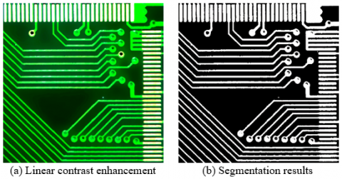
The same object was used for the experiments, as shown in Figure 3, which had been processed using the bilateral filtering. The figure included solder mask, wiring region, pad region, etc., as well as a significant bright spot caused by dust particles.
Figure 3. PCB image to be segmented
3.1 Experimental results of the color space threshold segmentation algorithm
Linear contrast of the image was enhanced according to Formula (6), as shown in Figure 4(a), with α=1.5 and β=-100 as the parameter setting. Based on prior knowledge, the segmentation thresholds $U_{L^*}=[170,255], U_{a^*}=[35,130]$ and $U_{b^*}=[130,215]$ were selected. The segmentation results are shown in Figure 4(b), where the white corresponds to the segmented object region and the black corresponds to the background region. It can be seen that this method has basically segmented the object region, but many serrated small protrusions or depressions have been generated on the boundary, which interfered with the defect feature extraction. At the same time, the segmentation results were greatly affected by noise.
Figure 4. Results of the threshold segmentation algorithm in the CIE L*a*b* space
3.2 Experimental results of the morphological edge detection segmentation algorithm
The image brightness component in the CIE L*a*b* space was extracted, as shown in Figure 5(a). Different structuring elements with the size of 3×3 were used for morphological edge extraction of the image, as shown in Figure 5(b) to Figure 5(d). The corresponding three structuring elements were cross-shaped, rectangular, and circular. It can be seen that the algorithm has better edge processing effects than the threshold segmentation algorithm. However, the color difference within the same region significantly affected the detection, easily leading to edge misdetection. At the same time, structuring elements in different shapes caused different segmentation results, indicating that the algorithm was greatly influenced by human factors.
Figure 5. Results of the morphological edge detection segmentation algorithm
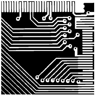
3.3 Experimental results of the K-means clustering segmentation algorithm
Image pixels were classified into clusters according to the algorithm steps, which obtained three cluster centers, as shown in Table 1. The brightness center $\overline{\boldsymbol{L}^*}$ of different clusters satisfied certain size relationships. Therefore, based on previous analysis, it was determined that Cluster 1 corresponded to the pad region pixels, Cluster 2 corresponded to the wiring layer region pixels, and Cluster 3 corresponded to the solder mask pixels. In addition, clusters 1 and 2 were merged. The final segmentation results are shown in Figure 6, where the white corresponds to the object region composed of the wiring layer and the pad, and the black represents the background region. It can be seen from the figure that the segmentation algorithm has the best effects. The clustering algorithm made adaptive adjustments, and the boundaries among different regions were clear and reliable. In addition, the algorithm had better partition consistency than the color space threshold segmentation algorithm, without significant serrated particle phenomenon. Meanwhile, compared with the morphological edge detection segmentation algorithm, the color instability in the same region did not affect the results of the clustering segmentation algorithm.
Table 1. Cluster centers obtained by the K-means clustering algorithm
|
No. |
$\overline{\boldsymbol{L}^*}$ coordinate |
$\overline{\boldsymbol{a}^*}$ coordinate |
$\overline{\boldsymbol{b}^*}$ coordinate |
|
Cluster 1 |
252 |
123 |
143 |
|
Cluster 2 |
209 |
52 |
198 |
|
Cluster 3 |
69 |
94 |
157 |
Figure 6. Results of the K-means clustering segmentation algorithm
Combined with the characteristics of PCB color images, this study analyzed the limitations of RGB color model on image processing, and chose to preprocess the images in the CIE L*a*b* color space. Bilateral filtering algorithm was used to reduce the image noise, which effectively protected the image edge details. The K-means clustering algorithm was chosen to accurately segment the wiring layer and pad regions in the image to reduce the subsequent amount of calculation, after comparing the three segmentation algorithms, namely, color space threshold segmentation, morphological edge detection segmentation, and K-means clustering segmentation. The experiments showed that the K-means clustering segmentation algorithm obtained the optimal segmentation results of PCB images, which classified and labeled all pixels according to the clustering results, extracted regions of interest as the research objects of subsequent defect feature extraction and detection, thus reducing the amount of calculation. However, the image itself was still a color image, i.e., all pixels still retained complete color information. Therefore, the image was used by the defect feature extraction algorithm, which effectively segmented regions of interest, such as the wiring layer and pad regions, thus ensuring that high quality images were used as the input of the defect detection algorithm.
This paper was supported by 2023 Youth Research Fund Project of Zhengzhou University of Economics and Trade (Grant No.: QK2111); 2022 Youth Research Fund Project of Zhengzhou University of Economics and Trade (Grant No.: QK2228); 2022 First Batch of Ministry of Education Industry-University Cooperation and Collaborative Education Projects (Grant No.: 220602693285155); 2022 Second Batch of Ministry of Education Industry-University Cooperation and Collaborative Education Projects (Grant No.: 220902693235012); 2022 Educational Reform Project of Zhongyuan University of Technology (Grant No.: 2022ZGJGLX017), 2022 Second Batch of Ministry of Education Industry-University Cooperation and Collaborative Education Projects (Grant No.: 220902693232323) and 2023 Key Scientific Research Project of Universities in Henan Province (Grant No.: 23B413003); Key Teacher Program of Zhengzhou University of Economics and Business (Grant No.: 2019ggjs02).
[1] Wu, Y.Q., Zhao, L.Y., Yuan, Y.B., Yang, J. (2022). Research status and the prospect of PCB defect detection algorithm based on machine vision. Chinese Journal of Scientific Instrument, 43(8): 1-17. http://dx.chinadoi.cn/10.19650/j.cnki.cjsi.J2209701
[2] Tu, Z.M., Wang, S.J., Shen, Z.W. (2022). PCB detection and sorting system based on machine vision. Modern Electronics Technique, 45(14): 5-9. http://dx.chinadoi.cn/10.16652/j.issn.1004-373x.2022.14.002
[3] Ma, J., Wang, C. (2022). Research on printed circuit board defect detection based on improved YOLOv4-tiny algorithm. Electronic Measurement Technology, 45(23): 99-106. http://dx.chinadoi.cn/10.19651/j.cnki.emt.2209991
[4] Huang, L., Shen, S., Xie, F., Zhao, J., Han, J., Feng, K. (2019). A novel multi-pattern solder joint simultaneous segmentation algorithm for PCB selective packaging systems. International Journal of Pattern Recognition and Artificial Intelligence, 33(13): 2058005. https://doi.org/10.1142/S0218001420580057
[5] Peng, C., Zou, J., Liang, M., Zhang, Z., Xu, H., Zhang, Z. (2020). A novel linear CCD variable velocity two-dimensional imaging approach based on adaptive image segmentation. IEEE/ASME Transactions on Mechatronics, 25(2): 762-769. https://doi.org/10.1109/TMECH.2020.2975096
[6] Gao, T., Feng, P. (2019). Research on image segmentation algorithm based on area array camera PCB automatic optic inspection. IOP Conference Series: Earth and Environmental Science, 252(3): 032104. https://doi.org/10.1088/1755-1315/252/3/032104
[7] Wang, S.Y., Zhao, Y., Wen, L.Y (2016). PCB welding spot detection with image processing method based on automatic threshold image segmentation algorithm and mathematical morphology. Circuit World, 42(3): 97-103. https://doi.org/10.1108/CW-08-2015-0039
[8] Pham, T.T.A., Thoi, D.K.T., Choi, H., Park, S. (2023). Defect detection in printed circuit boards using semi-supervised learning. Sensors, 23(6): 3246. https://doi.org/10.3390/s23063246
[9] Niu, J., Li, H., Chen, X., Qian, K. (2023). An improved YOLOv5 network for detection of printed circuit board defects. Journal of Sensors, 2023: 7270093. https://doi.org/10.1155/2023/7270093
[10] Qiao, N., Xiao, K., Wei, C. (2018). PCB photoelectric image circle detection based on improved Hough transform. Recent Advances in Electrical & Electronic Engineering (Formerly Recent Patents on Electrical & Electronic Engineering), 11(4): 457-459. https://doi.org/10.2174/2352096511666180213115737
[11] Liang, Q., Long, J., Nan, Y., Coppola, G., Zou, K., Zhang, D., Sun, W. (2019). Angle aided circle detection based on randomized Hough transform and its application in welding spots detection. Mathematical Biosciences and Engineering, 16(3): 1244-1257. https://doi.org/10.3934/mbe.2019060
[12] Hassanin, A.A.I., Abd El-Samie, F.E., El Banby, G.M. (2019). A real-time approach for automatic defect detection from PCBs based on SURF features and morphological operations. Multimedia Tools and Applications, 78: 34437-34457. https://doi.org/10.1007/s11042-019-08097-9
[13] Volkau, I., Mujeeb, A., Dai, W., Erdt, M., Sourin, A. (2021). The impact of a number of samples on unsupervised feature extraction, based on deep learning for detection defects in printed circuit boards. Future Internet, 14(1), 8. https://doi.org/10.3390/fi14010008
[14] Zhang, Q., Zhang, M., Gamanayake, C., Yuen, C., Geng, Z., Jayasekara, H., Woo, C.W., Low, J., Liu, X., Guan, Y. L. (2022). Deep learning based solder joint defect detection on industrial printed circuit board X-ray images. Complex & Intelligent Systems, 8(2): 1525-1537. https://doi.org/10.1007/s40747-021-00600-w
[15] Bártová, B., Bína, V. (2022). A novel data mining approach for defect detection in the printed circuit board manufacturing process. Engineering Management in Production and Services, 14(2): 13-25. https://doi.org/10.2478/emj-2022-0013
[16] Jiang, L., Wang, Z., Ye, Y., Jiang, J. (2018). Fast circle detection algorithm based on sampling from difference area. Optik, 158: 424-433. https://doi.org/10.1016/j.ijleo.2017.12.064
[17] Aversano, G., Esposito, A. (2002). Automatic parameter estimation for a context-independent speech segmentation algorithm. In Text, Speech and Dialogue: 5th International Conference, TSD 2002 Brno, Czech Republic, pp. 293-300. https://doi.org/10.1007/3-540-46154-X_40
[18] Xu, W., Thomasson, J.A., Su, Q., Ji, C., Shi, Y., Zhou, J., Chen, H. (2022). A segmentation algorithm incorporating superpixel block and holistically nested edge for sugarcane aphids images under natural light conditions. Biosystems Engineering, 216: 241-255. https://doi.org/10.1016/j.biosystemseng.2022.02.011
[19] Mehrabi, P., Taghirad, H.D. (2021). A novel gaussian process based ground segmentation algorithm with local-smoothness estimation. arXiv preprint arXiv:2112.05847