Impact of CuCl2 Addition to PMMA Polymer on Structural and Optical Properties

Saba Abdulzahra Obaid Alshiaa*![]() | Alyaa Hefdhi Abbas Aziz | Inass Abdulah Zgair
| Alyaa Hefdhi Abbas Aziz | Inass Abdulah Zgair![]() | Nahida B.Hasan
| Nahida B.Hasan![]()
© 2024 The authors. This article is published by IIETA and is licensed under the CC BY 4.0 license (http://creativecommons.org/licenses/by/4.0/).
OPEN ACCESS
Pure and CuCl2 Poly(methyl methacrylate) (PMMA) films have been prepared by the solution cast method. The morphology of the films was investigated by atomic force microscopy (AFM). The roughness, grain size, and average diameter of the pure and doped samples vary between an increase and a decrease with an increase the doping concentration. The root mean square (RMS) roughness of the dope of copper nanoparticle CuCl2 on the PMMA polymer was studied from 3D AFM images,increases from (5.27) nm to (10.42) nm. The homogeneity of the surface grains rises with the inuction in the value of the roughness rate with an increase in the dope. The optical characteristics of the polymer films were analyzed in the (200-1200) nm wavelength range. The transmittance, absorption coefficient, band gap, and Urbach have been estimated. The value of the energy band gap was 3.72 eV for an an undoped sample and it has been decreased to be (3.3, 3.23, and 3.19) eV for (1, 2 and 3) % of the doping ratio of CuCl2 while Urbach energy was increased after dopping.
PMMA polymer, copper choride II, casting method, spectroscopy, thin film, AFM
Polymers are important materials in a variety of applications, including rubber, plastics, resins, and adhesive. The phrase "polymer" is derived from the Greek terms "poly," which means "many," and "mers," which refers to components or units of large molecular mass [1]. These components are often linked together to form huge molecules known as macromolecules. Polymers are classed according to their physical qualities, such as solubility [2]. They are characterised as hydrophobic polymers, which have a low water solubility, or polymers with hydrophilic properties, which have a high water solubility and the thermal behaviour of polymers, such as thermoplastics [3]. Thermoplastics can was soften when heated and may be moulded again, but thermosetting polymers suffer irreversible cross-linking when heated and cannot be reshaped [4]. The nanocomposites PMMA-based are a class of materials that are formed by the incorporation of nanoscale particles into a PMMA matrix [5]. The nanoparticles can be metallic, ceramic, or organic, and they are typically in the range of 1-100 nm in size. PMMA is a commonly used polymer due to its high transparency, good chemical resistance, and ease of processing [6]. However, the properties of PMMA can be improved by incorporating nanoparticles into the matrix. PMMA-based nanocomposites have several applications in electronics, optics, and biomedical engineering [7].
A polymer's physical characteristics, such as glass transition temperature (Tg), solubility, crystallinity and hydrolysis are determined not only by the kind of monomer used, but also by secondary and tertiary structures. Based on this fundamental chemistry, PMMA could be isotactic, syndiotactic, or a tactic [8, 9]. Copper nanoparticles are exploited in a range of applications due to their unique properties such as increased surface area to volume ratio, higher catalytic activity and enhanced electrical conductivity [10]. Copper nanoparticles are able to be manufactured by numerous ways such as chemical reduction, electrochemical depositing, and laser ablation [11]. They've found use in fields including electronics, energy, and biology. Copper nanoparticles are utilised as conductive inks in electronics to print flexible circuits. Copper nanoparticles are employed as catalysts in the energy industry to convert carbon dioxide into fuel [12]. Polymer composites are made by strengthening and incorporating dopant elements into the polymer matrix, resulting in improved electrical, optical, and mechanical characteristic [13]. These characteristics are substantially impacted by a variety of parameters, including the composition of the polymer matrix, doping concentration, and the interaction between the polymer and doping elements [14, 15].
This study's findings can also add to current information by offering a better understanding of the behaviour of copper nanoparticle doped PMMA polymer at various temperatures. The research can help to construct theoretical models that can anticipate the behaviour of the material under various processing circumstances.
Polymethyl methacrylate (PMMA) polymer with high purity (99.999%) were used as matrix polymeric materials in this work, As follows:
The PMMA polymer (13.69 gram) was dissolved in 70 ml of methyl solvent using mixing for a period of 35 minutes.
1) (17.4 gram) of copper Chloride IIIIis dissolved in 100 ml of distilled water for a period of 30 minutes
2) (1 ml) of (CuCl2) was added to 10 ml of polymer and mixed for 15 minutes
3) (2 ml) of (CuCl2) was added to 10 ml of polymer and mixed for 15 minutes
4) (3 ml) of (CuCl2) was added to 10 ml of polymer and mixed for 15 minutes
Films were fabricated from solutions by BYK Gardner GmbH applicator; the liquid layer had a thickness of 30, 60, and 90 μm, while the dry film had a thickness of 4, 7. Utilising titanium dioxide's (TiO2) catalytic characteristics, photocatalytic coatings are marketed as "self-cleaning" glass. Rainwater sticks to the glass, allowing it to "selfclean" when exposed to UV radiation, which makes the coating very hydrophilic. One product that has a photocatalytic coating that makes glass simpler to clean is Pilkington ActivTM Self-cleaning Glass. After that composite films (PMMA-CuCl2) were made on a petri dish by casting method of thickness (300 nm) at room temperature. casting method is a method of covering flat objects with a thin layer of homogenous coatings. A small amount of (PMMA-CuCl2) composite material is usually placed in the center of the substrate. Figure 1 demonstrates the method of preparing of (PMMA-CuCl2) composite films.
Figure 1. Method of preparation of (PMMA-CuCl2) composite films
Surface morphological measurements for PMMA polymer doped by (CuCl2) rate (1%, 2% and 3%) thin films with different temperature for (15 min), 2D and 3D images for all studied samples were get. The optical properties of (PMMA polymer doped by (CuCl2) rate (1%, 2% and 3%) thin films with different temperatures for (15 min) were studied in the wavelength range (300-800) nm by using UV/Vis (1800I) spectrophotometer. These spectrometers contains two light sources Deuterium and Tungsten lamp within the wavelengths range (190-1100) nm of the spectrum.
4.1 Atomic force microscope of (PMMA-CuCl2) composite film
AFM images analysis is aim to obtain accurate information about the surface and give the statistical values with high accurateness about the poreaverage diameter, roughness average, and root means square (RMS). Through microscopic analysis (AFM), we can learn about the differences in inhomogeneity features or attributes linked to each atom individually, as well as an illustration of the crystalline size distribution rate onto surfaces [16]. The surface morphology of CuCl2 thin films doping by rate (1, 2, and 3%) were determined by Atomic Force Microscope (AFM), average roughness were tabulated in Table 1 which shows the roughness increase with doping rates increase. Figure 2 displays AFM images of the films coated on glass substrate indicated densely packed and uniform size crystallites somewhat. The images assure that PMMA films have a smooth surface morphology decreasing with CuCl2 doping increasing. The decrease of surface roughness was assigned to larger grain formation. Figure 2 offers Rrms, particle size, and 3D surface morphology. As you can be seen the Rrms and D depend on doping. The Rrms value of )5.72) nm for as deposited CuCl2 thin films decreased to )2.42) nm by increasing of doping, except when the concentration of the CuCl2 activator increases [17].
Figure 2. 2D AFM images with different doping rates for (PMMA-CuCl2) composite film
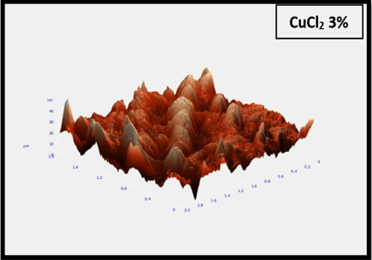
Figure 3. 3D AFM images with different doping rates for(PMMA-CuCl2) composite film
The root mean square (RMS) roughness of the dope of copper nanoparticle CuCl2 on the PMMA polymer was studied from 2D and 3D AFM images shows in Figures 2, 3, the RMS values were calculated from height values in the atomic force microscopy.
Table 1. AFM measurements for deferent doping rate of (PMMA-CuCl2) composite film
|
Doping Rates (percent) |
Grain Size (nm) |
Roughness(nm) |
D (nm) |
|
0 |
55.31 |
5.72 |
8.02 |
|
1% |
50.11 |
5.61 |
7.25 |
|
2% |
21.16 |
2.42 |
3.61 |
|
3% |
82.43 |
10.42 |
15.37 |
4.2 The optical properties of (PMMA-CuCl2) composite films
To investigate the optical properties, a UV-Vis spectrophotometer was used in the range of wavelength (200-1200) nm. The transmittance spectra of pure and doped PMMA film show that the transparency of PMMA film decreased with an increase in the doping concentration and the absorption edge was shifted toward a longer wavelengths (redshift) as shown in Figure 4 and this behavour closed to that obtained by Gupta et al. [18].
Figure 4. Transmittance spectra for (PMMA-CuCl2) composite film with different doping rate
Figure 5 illustrates the spectra of absorbance of un-doped and (1, 2, and 3) % doped CuCl2 thin films. From the Figure, it can be seen that an increase in the absorption reveals that the films become translucent to visible light [19].
Figure 5. Absorbance spectra for (PMMA-CuCl2) composite film with different doping rate
Figure 6 displays the plot of $(\alpha h v)^2$ vs $h v$ for various dopant concentrations in polymer samples. The behavior seen indicates that amorphous material may have been permitted to transition. The energy band gap (Eg) of undoped and PMMA: CuCl2 samples were evaluated utilizing Tauc's formula [20].
$\alpha h v=G\left(h v-E_g\right)^\gamma$ (1)
where, $\alpha$ denoted to absorption coefficient $G$ is the independent constant of energy , the exponent $\gamma$ define to the optical transition nature where if; =1/2, 3/2, for direct allowed and direct forbidden transition while and $\gamma$=2 and 3 indirect allowed as well as indirect forbidden transition respectively.
The optical energy gap values obtained through extrapolation of the linear area have been determined to be reducing for all samples (3.72, 3.3, 3.23, and 3.19) eV with increase dopant concentration of CuCl2 (0, 1, 2 and 3) %. The energy gap values decrease with increments dopant percentage of CuCl2 this might be due to the generation of new localized levels in the band gap. When the Eg value is low, electrons require less energy to transfer from the valence band to the conduction band and comprehended by analyzing the variation in the mobility gap in the doped polymer [21-23].
Figure 6. Direct energy band gap for (PMMA-CuCl2) composite film with different doping rate
The Urbach energy (EU) is an indication of the localized density of states that stretch into the band gap and mostly caused by impurities, noncrystalline energy, and defects. The value of EU, is obtained as the reciprocal of the slopes of the linear section below the optical band gap when plotting ln $\alpha$ vs $\mathrm{h} \nu$ and can be calculated from the formula [24]:
$\alpha=\alpha_0 \exp \frac{h v}{E_U} \rightarrow E_U=\left[\frac{d \ln \alpha}{d h v}\right]^{-1}$ (2)
where, $\alpha_0$ is a constant and hʋ photon energy.
Figure 7 shows the increase in the $E_U$ values after the doping process might owing to the presence impurities , defects and increasing the amorphous nature [25, 26].
Figure 7. Urbach energy of (PMMA-CuCl2) film with different doping rate
Also, Figure 8 illustrates the reflectance spectra with thickness (300) nm .simply it is shown that the reflectance spectra are higher in B bands. The minimum reflectance appears at undoping rate (pure) and increases with increasing the doping rate (1, 2, and 3%).
Figure 8. Reflectance spectra for (PMMA-CuCl2) composite film with different doping rate
The percentage of light lost as a result of scattering and absorption per unit distance of the penetrating medium is measured by the extinction coefficient. It can be calculated using the relation from the values of $\alpha$ and $\lambda$ [27].
$\mathrm{K}=\frac{\alpha \lambda}{4 \pi}$ (3)
The increase in k value shown in Figure 9 might attributed to the influence of CuCl2 on the structure of PMMA which lead to the generate of localized energy state in forbidden band gap behaves as tails to the conduction band then decreased the energy gap (Eg) [28] and this raising in k value corresponded with that obtained by AFM measurement and energy gap analysis.
Figure 9. Extinction coefficient for (PMMA- CuCl2) composite film with different doping rate
The imaginary and real part of dielectric constant as Figure 10 shows display an increase on increasing the ratio of doping percentage similar to that results data obtained by Gupta et al. [18].
The dielectric constant with both its imaginary $\left(\varepsilon_i\right)$ and real $\left(\varepsilon_{\mathrm{r}}\right)$ parts as Figure 11 shows can be evaluated by the formula [29]:
$\varepsilon_i=2 n k$ (4)
$\varepsilon_r=n^2-k^2$ (5)
Figure 10. Real part of dielectric constant for (PMMA-CuCl2) composite film with different doping rate
Figure 11. Image part of dielectric constant for (PMMA-CuCl2) composite film with different doping rate
In general, the study focus on pure and PMMA doped CuCl2 films, which were primed using the casting method. The consequences showed that roughness, grain size, and average diameter films experienced an decrease in intensity after adding various concentration of CuCl2 leading to in the appearance of many peaks clumered vertically onto substrate [17]. The effects of the change in the doping ratio of CuCl2 on the optical characteristics of the films were carefully analyzed. The energy band gap had illustrated a reduction after adding CuCl2 while Urbach energy and transperancy have been increase [25]. In addition that optical constants such as reflectance, extinctin coefficient and real and imaginary dielectric constants have been increased after doping process.
[1] Tuttle, M.E. (1999). A brief introduction to polymeric materials. University of Washington: Seattle, WA, USA.
[2] Alves, T.F., Morsink, M., Batain, F., Chaud, M.V., Almeida, T., Fernandes, D.A., da Silva, C.F., Souto, E.B., Severino, P. (2020). Applications of natural, semi-synthetic, and synthetic polymers in cosmetic formulations. Cosmetics, 7(4), 75. https://doi.org/10.3390/cosmetics7040075
[3] Srivastava, S., Haridas, M., Basu, J.K. (2008). Optical properties of polymer nanocomposites. Bulletin of Materials Science, 31: 213-217. https://doi.org/10.1007/s12034-008-0038-9
[4] Dmour, I., Taha, M.O. (2018). Natural and semisynthetic polymers in pharmaceutical nanotechnology. Organic Materials as Smart Nanocarriers for Drug Delivery, 35-100. https://doi.org/10.1016/B978-0-12-813663-8.00002-6
[5] Pal, K. (2016). Effect of different nanofillers on mechanical and dynamic behavior of PMMA based nanocomposites. Composites Communications, 1: 25-28. https://doi.org/10.1016/j.coco.2016.08.001
[6] Placido, A.J. (2010). Characterization of poly (methyl methacrylate based nanocomposites enhanced with carbon nanotubes. Doctoral dissertation, University of Kentucky Libraries.
[7] Ji, W.F., Chang, K.C., Lai, M.C., Li, C.W., Hsu, S.C., Chuang, T.L., Yeh, J.M., Liu, W.R. (2014). Preparation and comparison of the physical properties of PMMA/thermally reduced graphene oxides composites with different carboxylic group content of thermally reduced graphene oxides. Composites Part A: Applied Science and Manufacturing, 65: 108-114. https://doi.org/10.1016/j.compositesa.2014.05.017
[8] Ali, U., Karim, K.J.B.A., Buang, N.A. (2015). A review of the properties and applications of poly (methyl methacrylate)(PMMA). Polymer Reviews, 55(4): 678-705. https://doi.org/10.1080/15583724.2015.1031377
[9] Kh. K. Reham, “Effect of Beta particles irradiation on structural and optical properties of metal – phthalocyanine thin films supervised by,” Babylon, 2022.
[10] Song, X., Sun, S., Zhang, W., Yin, Z. (2004). A method for the synthesis of spherical copper nanoparticles in the organic phase. Journal of Colloid and Interface Science, 273(2): 463-469. https://doi.org/10.1016/j.jcis.2004.01.019
[11] Din, M.I., Rehan, R. (2017). Synthesis, characterization, and applications of copper nanoparticles. Analytical Letters, 50(1): 50-62. https://doi.org/10.1080/00032719.2016.1172081
[12] Hasan, N.B., Mohammed, M.A. (2017). XRD investigation of (PbO)1-x(CdO)x thin films deposited by spray pyrolysis technique. Journal of Babylon University/Pure and Applied Sciences, 2(25): 544-552.
[13] Saini, I., Rozra, J., Chandak, N., Aggarwal, S., Sharma, P.K., Sharma, A. (2013). Tailoring of electrical, optical and structural properties of PVA by addition of Ag nanoparticles. Materials Chemistry and Physics, 139(2-3): 802-810. https://doi.org/10.1016/j.matchemphys.2013.02.035
[14] Haroun, A.A., Kamel, S., Elnahrawy, A.M., Hammad, A.A., Hamadneh, I., Al-Dujaili, A.H. (2020). Polyacetal/graphene/polypyrrole and cobalt nanoparticles electroconducting composites. International Journal of Industrial Chemistry, 11: 223-234. https://doi.org/10.1007/s40090-020-00218-w
[15] Abdel-Fattah, E., Alharthi, A.I., Fahmy, T. (2019). Spectroscopic, optical and thermal characterization of polyvinyl chloride-based plasma-functionalized MWCNTs composite thin films. Applied Physics A, 125(7): 475. https://doi.org/10.1007/s00339- 019-2770-y
[16] Read, D.T., Volinsky, A.A. (2007). Thin films for microelectronics and photonics: Physics, mechanics, characterization, and reliability. In Micro-and opto-electronic materials and structures: Physics, mechanics, design, reliability, packaging, pp. A135-A180. http://doi.org/10.1007/0-387-32989-7_4
[17] Patil, V.T., Toda, Y.R., Joshi, V.P., Tayade, D.A., Dhanvij, J.V., Gujarathi, D.N. (2013). Surface morphological and optical properties of CdSe thin films by closed space sublimation technique. Chalcogenide Letters, 10(7): 239-247.
[18] Gupta, A.K., Bafna, M., Vijay, Y.K. (2018). Study of optical properties of potassium permanganate (KMnO4) doped poly (methylmethacrylate)(PMMA) composite films. Bulletin of Materials Science, 41(6): 160. http://doi.org/10.1007/s12034-018-1654-7
[19] Soni, G., Soni, P., Jangra, P., Vijay, Y.K. (2019). Optical, mechanical and thermal properties of PMMA/graphite nanocomposite thin films. Materials Research Express, 6(7): 075315. http://doi.org/10.1088/2053-1591/ab1327
[20] Tauc, J. (1974). Amorphous and liquid semiconductors. Plenum Press, USA.
[21] Najeeb, H.N., Balakit, A.A., Wahab, G.A., Kodeary, A.K. (2014). Study of the optical properties of poly (methyl methaacrylate)(pmma) doped with a new diarylethen compound. Academic Research International, 5(1): 48.
[22] Tan, K., Samylingam, L., Aslfattahi, N., Johan, M.R., Saidur, R. (2022). Investigation of improved optical and conductivity properties of poly (methyl methacrylate)–MXenes (PMMA–MXenes) nanocomposite thin films for optoelectronic applications. Open Chemistry, 20(1): 1416-1431. https://doi.org/10.1515/chem-2022-0221
[23] Oboudi, S.F., Yousif, E., Abdul Nabi, M., Yusop, R.M., Derawi, D. (2015). Fabrication and characterization of nickel chloride doped PMMA films. Advances in Materials Science and Engineering, 2015: 913260. https://doi.org/10.1155/2015/913260
[24] Lakhdar, M.H., Ouni, B., Amlouk, M. (2014). Thickness effect on the structural and optical constants of stibnite thin films prepared by sulfidation annealing of antimony films. Optik, 125(10): 2295-2301. https://doi.org/10.1016/j.ijleo.2013.10.114
[25] Alsaad, A., Al Dairy, AR., Ahmad, A., Qattan, I.A., Al Fawares, S., Al-Bataineh, Q. (2021). Synthesis and characterization of polymeric (PMMA-PVA) hybrid thin films doped with TiO2 nanoparticles using dip-coating technique. Crystals, 11(2): 99. https://doi.org/10.3390/cryst11020099
[26] Aziz, S.B., Abdullah, O.G., Hussein, A.M., Ahmed, H.M. (2017). From insulating PMMA polymer to conjugated double bond behavior: Green chemistry as a novel approach to fabricate small band gap polymers. Polymers, 9(11): 626. https://doi.org/10.3390/polym9110626
[27] Sze, S.M., Li, Y., Ng, K.K. (2021). Physics of Semiconductor Devices. John Wiley & Sons.
[28] Mohi, A.T. (2019). Optical energy gap and optical constants of poly (Methyl methacrylate) films doped with ZnCl2. Internaptional Journal of Advanced Scientific Research, 4(3): 35-37.
[29] DrDomenico Jr, M., Wemple, S.H. (1969). Oxygen‐octahedra ferroelectrics. I. Theory of electro‐optical and nonlinear optical effects. Journal of Applied Physics, 40(2): 720-734. https://doi.org/10.1063/1.1657458