Influence of Annealing Process on Cu2O Nanofilm and the Efficiency of Annealed p-Cu2O/n Si Nanostructure Solar Cell Prepared by Thermal Evaporation Technique

Inass Abdulah Zgair*![]() | Abdulazeez O. Mousa Al-Ogaili
| Abdulazeez O. Mousa Al-Ogaili![]() | Khalid Haneen Abass
| Khalid Haneen Abass![]()
© 2024 The authors. This article is published by IIETA and is licensed under the CC BY 4.0 license (http://creativecommons.org/licenses/by/4.0/).
OPEN ACCESS
Thin film solar cells are one of the significant electronic applications due to their beneficial characteristics, especially adjustable optical features low cost, and high efficiency. In this research, p-type cupric oxide (Cu2O) nanofilms have been successfully deposited onto glass and n-type Si substrates by thermal evaporation technique under 10-7 mbar, rate of deposition of 0.3 nm/s after that annealed at 200℃. The annealing process leads to an increase in the uniformity and homogeneity distribution of particles on the thin film surface as well as an improvement of the roughness. FE-SEM images of Cu2O nanofilms show that the average size has been increased from 25.15 to 35.36 with the enhancement of the distribution of particles after the annealing process. Average roughness and root mean square have increased from (0.166 to 1.18) nm and (0.213 to 1.490) nm respectively. Electrical characteristics of annealed Al/ Cu2ONPs/Si/Al solar cell were examined by current-voltage measurement. The short circuit current (ISC.) of 15 mA, open circuit voltage (VOC) of 500 mV, fill factor (F.F) of 0.45, and the efficiency (η) was found to be 3.37%. The annealing temperature gives more roughness to the surface and raises the absorption of incident photons and solar cell efficiency.
annealing, cuprous oxide, nanofilm, solar cell, thermal evaporation
The investigation of unique oxide semiconductors was intensified in the previous two decades, mostly by solar cell applications or transparent electronics. In the category of p-type semiconducting substances, cuprous oxide (Cu2O) exhibits intriguing electrical and industrial characteristics that make it an appropriate candidate for energy and electronic devices [1, 2]. Cu2O is an appropriate choice because of the high absorption coefficient it has, the high hole mobility it possesses, the quantity of its constituent elements in the crust of the earth, and the fact that it is non-toxic [3-5]. Cu2O is a stable binary copper oxide crystallizing in a cubic structure with a space group (Pn-3m) with the value of a lattice constant about 4.269Å where the unit cell consists of about four copper atoms and two oxygen atoms [6, 7]. It exhibits a direct optical bandgap from 2.10 to 2.60 eV [8, 9]. The Cu2O thin film could be manufactured utilizing a variety of different chemical and physical processes, such as the chemical deposition technique [10], thermal oxidation [11], spin coating [12], plasma evaporation [13], molecular beam epitaxy [14], radio frequency (RF) [15] spray pyrolysis technique [16]. Tuama et al. [17] prepared Cu2O: Ag NPs/Si solar cell by the technique of thermal evaporation and the conversion efficiency that they obtained of 3.5 by Cu2O: 0.04 Ag NPs/Si. Jayathilaka et al. [18] deposited Cu2O homojunction thin film onto a Ti substrate by an electrochemical deposition technique and the gained conversion efficiency of 2.64%, under AM1.5 illumination, were achieved by an annealed sulfur-treated solar cell of Ti/n-Cu2O/p-Cu2O/Au. Abdurrahman et al. [19] fabricated a photoactive substance comprising of Bi/Cu2O/Bi solar cell by using a thermal oxidation process and method of powder vaporization, and the fabricated cell produced a power conversion efficiency of 1.14%.
The aim of this work is to enhance the value of efficiency of p-Cu2ONPs/n-Si solar cell after the annealing process at 200℃. Cu2O nanofilms were fabricated on a glass substrate by using an effective thermal evaporation method in order to study the structural and surface morphology with respect to the annealing process as well as Cu2O nanofilms deposited onto n-type silicon substrate to fabricate Al/Cu2ONPs/Si/Al solar cells where pure aluminum that coated onto Cu2O/Si nanofilms allows for the production of the front and back contacts of the solar cell. There are many challenges in manufacturing solar cells such as the choice of appropriate material and the cost of production as well as the method of manufacturing solar cell.
In this research, employed the method of thermal evaporation because of large-area coating, simple, effective and low coast technique.
Cu2O nanofilms were formed onto substrates of glass and n-type silicon via the technique of thermal evaporation. The glass substrates were ultrasonically cleaned with acetone, distilled water, then ethanol, and finally water in order to remove dirt and oil. The Cu2O powder was used because of it low cost, nontoxic as well as the high absorption coefficient almost nearly identical to the solar radiation optimal value. Cu2O powder was put into the boat of tungsten in the vacuum chamber. During the coating process, a pressure of 10-7 mbar was obtained and maintained at that level in the vacuum chamber, which facilitates the metal's evaporation and further transports it to the substrate. The rate of the coating was 0.3 nm/s in order to create a very thin layer for Cu2O nanofilm. Evaporation of the material was accomplished with the assistance of the power source, and the material that had been vaporized was eventually condensed on the glass and Si substrates. The deposited films after that annealed for two hours at a temperature of 200℃. The annealing process of thin films was accomplished by the electrical furnace (CARBOLITE (CWF 1200) in order to enhancement the structural, morphology and electrical characteristics of Cu2O nanofilms. The morphology of the surface of Cu2O nanofilms was inspected via an atomic force microscope (Aα3000 SPM)) and field emission scanning electron microscopy (INSPECT- 550) to study topography. The electrical characteristics were examined by (Ecola, Hall Effect Measurement System, HMS-3000) and the heterojunction characteristics of Cu2ONPs/n-Si were examined via calculated the illuminated and dark I–V characteristics by (Keithley 177 Micrometer Dmm System).
These equipment’s was used to help in offering an understanding topographical, structural and electrical characteristics of nanofilm surface and electronic transitions and how they are employed effectively in solar cell applications. Solar Cell I-V Characteristics Curves are basically a graphical representation of the operation of a solar cell summarizing the relationship between the current and voltage at the existing conditions of irradiance and temperature. The power delivered by a single solar cell is the product of its output current and voltage (Im x Vm). The span of the solar cell I-V characteristics curve ranges from the short circuit current (Isc) at zero output volts, to zero current at the full open circuit voltage (Voc). In other words, the maximum voltage available from a cell is at open circuit and the maximum current at closed circuit.
Depositing pure aluminum on the Cu2O/Si films allows for the production of the front and back contacts of the solar cell, which is necessary for the manufacture and characterization of p-n junction devices.
The morphology and electrical characteristics of the Cu2O nanofilms as-fabricated and annealed onto glass and substrate via technique of thermal evaporation and annealed at 200℃ were examined. Hall parameters and some important parameters of Cu2ONPs/Si solar cell were evaluated such as open circuit voltage (Voc), short circuit current (Isc), fill factor (F.F), and efficiency (η).
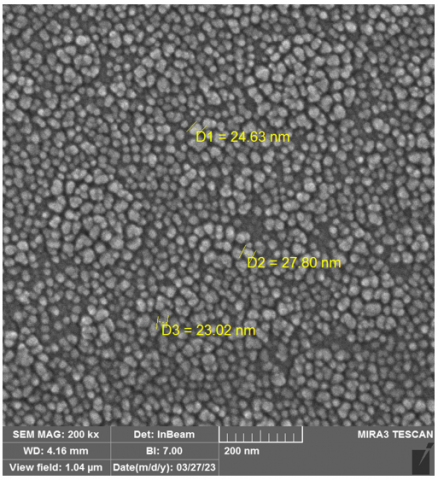
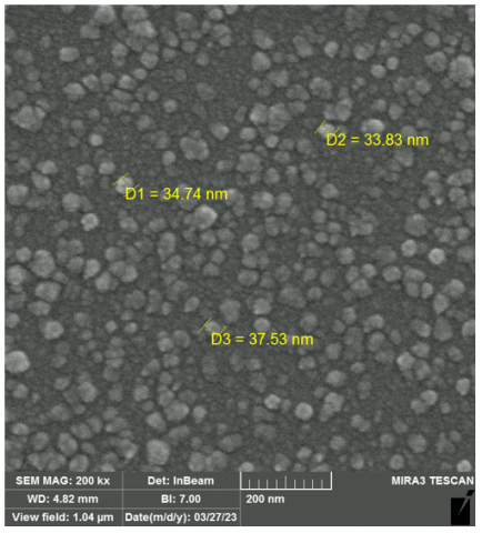
Figure 1(a) shows FE-SEM image of Cu2O/glass nanofilm as deposited showing circular assemblies of grains including large and small particles, with irregular distribution onto the surface of the thin film, whereas the particles seem elongated on the surface with an average size of approximately 25.15 nm. Figure 1(b) illustrates FESEM images of Cu2O/glass nanofilm thin film when annealed at 200℃ for 2h. FESEM images reveal a homogenous and uniform surface with no discernible micro-cracks, and the morphology of the produced films demonstrates that the particle size increases with rising temperature by the annealing process with an average grain size of around 35.36 nm and this could be due to the improvement of the crystallinity of Cu2O nanofilms by the annealing process and the reduction in its crystal imperfections [20].
(a)
(b)
Figure 1. FESEM images of: (a) Cu2O/glass nanofilms as prepared and (b) Cu2O nanofilms as annealed at 200℃
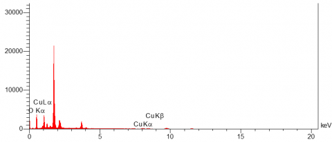
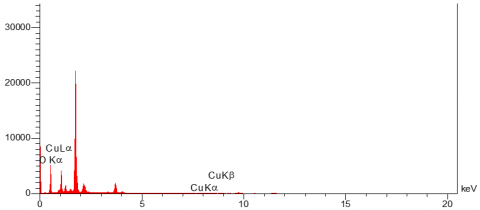
The basic aim of EDX measurement of a Cu2O/glass nanofilm is to prove the presence of the elements (copper, and oxygen) that comprise the structure of the thin film and show the variation of atomic ratio for copper and oxygen for prepared and annealed samples as listed in Table 1 and the main peaks of CuLa, CuKa, CuKb, and OKa lines clearly appear in Figure 2.
Table 1. EDX data of Cu2O/glass nanofilms before and after the annealing process
|
Samples |
Element |
Intensity |
Error |
K |
W% |
A% |
|
Deposited Cu2O nanofilm |
O |
414.6 |
68.39 |
0.956 |
94.87 |
98.66 |
|
Cu |
12.7 |
1.40 |
0.043 |
5.13 |
1.34 |
|
|
|
1.00 |
100 |
100 |
|||
|
Annealed Cu2O nanofilm |
O |
553.6 |
69.42 |
0.978 |
97.36 |
99.32 |
|
Cu |
8.1 |
0.65 |
0.021 |
2.64 |
0.68 |
|
|
|
1.00 |
100 |
100 |
|||
(a)
(b)
Figure 2. EDX spectra of Cu2O nanofilms: (a) as deposited and (b) annealed at 200℃ for 2h
Table 2. The AFM data of Cu2O/glass nanofilms
|
Sample |
Average Roughness (nm) |
Root Mean Square (nm) |
Average Diameter (nm) |
|
Deposited Cu2O nanofilm |
0.166 |
0.213 |
150.5 |
|
Annealed Cu2O nanofilm |
1.180 |
1.490 |
236.3 |
AFM analysis was employed to investigate the crystalline structure surface topography the thin film.
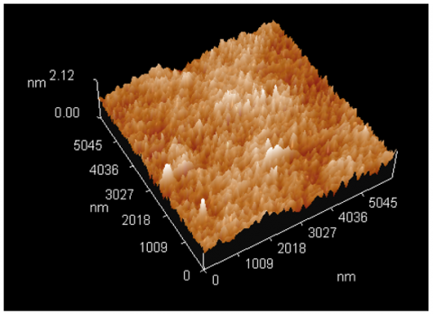
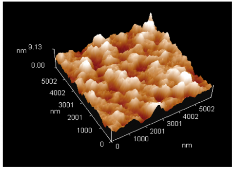
Figure 3 displays the AFM images of Cu2O nanofilms that were deposited onto glass substrate via the thermal evaporation method which have been post-annealed at 200℃. The deposited sample has a small number of sharp peaks that coalesce as islands vertically to the surface of the film. The values of roughness have increased from (0.166 to 1.180) nm may have been due to the formation of large grains as a consequence of the diffusion effect as a result of the annealing process [21]. This increase in roughness reveals the uniformity of the surface of the film and the opportunity of use in solar cells owing to its good reflection [22]. The root mean square attained from AFM measurements and its value raised from (0.213 to 1.490) nm as well as increased the average diameter from 150.5 nm to 236.3 nm after the annealing process, this might have been attributed to the increase in softness [22] as listed in Table 2.
(a)
(b)
Figure 3. AFM images of Cu2O/glass nanofilms: a) as-deposited and b) annealed films at 200℃
Table 3. Electrical data of Cu2O/glass nanofilm
|
Electrical Properties |
Deposited Cu2O Nanofilm |
Annealed Cu2O Nanofilm |
|
Carrier Type |
n-type |
p-type |
|
Resistivity (Ω cm) |
1.426E+5 |
2.598E+5 |
|
Hall Mobility (cm2 /Vs) |
1.056 E+2 |
7.229 E+1 |
|
Carrier Concentration (cm−3) |
-4.144 E+11 |
3.323 E+11 |
|
Average Hall Coefficient |
-1.506E+7 |
1.878E+7 |
|
Conductivity (Ω cm)-1 |
7.012E-6 |
3.849E-6 |
The electrical properties of deposited and annealed Cu2O/glass nanofilm are shown in Table 3. Increased temperature by the annealing process resulted in a rise in average Hall coefficient and electrical resistivity and this behaves close to that observed by Han et al. [23] and Yang et al. [24]. The carrier concentration of the film was decreased from (4.144×1011 cm−3 to 3.323×10¹¹) cm-3 which can be owing to the improvement of crystal quality and the reduced crystal defects [25]. The resistivity increased after the annealing process while conductivity decreased.
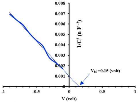
Figure 4. Built-in potential plots of annealed Cu2ONP/ n-Si
Capacitance-voltage measurement is one of the most important methods for obtaining information about the rectifying junctions, built-in potential, and junction capacitance and junction type [26]. Figure 4 gives the variation of (1/C2) vs (V) measurements for different samples. From these Figures, it can be seen that a straight line, of which the intercept with the voltage axis gives the value of the built-in potential and its value for annealed Cu2ONPs/n-Si heterojunction about 0.15 volt.
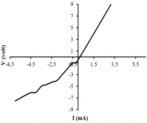
Current-voltage (I-V) curves can be used to determine the solar cell's efficiency of Cu2ONPs/n-Si in the dark and under illumination using a light source emitting 100 mW/cm2 with active area of the cell of 0.5×0.7 cm2. In the dark, there is a rectification behavior for the Cu2O/Si heterostructure as displayed in Figure 5 [27].
Figure 5. I-V Characteristics of Cu2ONPs/n-Si solar cell (under dark)
Figure 6 I-V curve of the created solar cell of Cu2ONPs/n-Si. As is apparent, the open circuit voltage (VOC) follows the theoretical path in which VOC increases with decreasing temperature. Eq. (1) describes the relationship between open circuit voltage and temperature [28].
$\mathrm{Voc}=\frac{K_{\mathrm{B}} T}{q} ln \frac{I_{\text {gen }}}{I_{\text {sat }}}+1$ (1)
The fill factor is a quantity that characterizes the solar cell's nonlinear electrical behavior. Most frequently, the fill factor is computed from measurements of the I-V curve as demonstrated by the equation [29].
$P_{\text {out }}=I_{\text {max }} V_{\text {max }}$ (2)
where, Imax, Vmax, and Pout are denoted as the maximum of current, voltage, and power, respectively.
$F F=\frac{{ Imax\,\, Vmax }}{ { Isc\,\, Voc }}$ (3)
The ratio of the photovoltaically produced output to the incident power falling on a solar cell is known as efficiency [30, 31].
$\eta=\frac{P_{\text {out }}}{P_{\text {in }}}=\frac{F F V_{o c} I_{s c}}{P_{\text {in }}} \times 100 \%$ (4)
where, Pin is incident power on the cell.
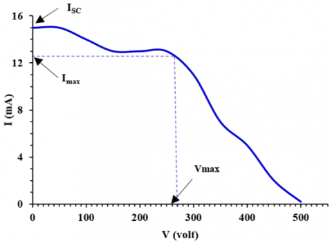
From (I-V) characteristics in Figure 6, VOC gets its value from the intersection of the measured current and the axis of applied voltage used, i.e. when the solar cell has a current equal to zero or when the external circuit is open. This value of voltage can be considered the maximum voltage that a solar cell can produce [32]. The static parameters of Cu2ONP/n-Si solar cells were as follows: All solar cells parameters were calculated from ISC of 12.5 mA, VOC of 500 mV, F.F of 0.45, and efficiency of around 3.37% This result is close to that obtained by Attia et al. [33]. This value of efficiency was obtained due to an increase in roughness and then increase in absorbance of the incident photons.
Figure 6. I-V Characteristics of Cu2ONP/ n-Si solar cell (under illumination)
Solar cells are one of the renewable energy sources, where solar energy is considered the most environment-friendly and cost-effective of all renewable energy sources, and it has the potential to provide an unlimited supply of energy with minimal environmental impact. This makes solar cell technology economically feasible and sustainable and enables possible reductions in greenhouse gas emissions, making it a perfect source of energy that avoids energy and environmental risks.
In this work, the morphology and electrical characteristics of the Cu2O nanofilm prepared by thermal evaporation technique and annealed at 200℃ onto glass and silicon substrates were studied. The FESEM images of Cu2O/glass nanofilm reveal that there is an increase in the size of the particle crystals after the annealing process. The morphology of the surface seems to be homogenous and uniform, with no discernible micro-cracks. AFM analysis shows an increase in roughness, root mean square, and average diameter when annealed at 200℃. Under illumination with a light source emitting 100 mW/cm2, this work was achieved in order to get solar cell parameters. The Al/Cu2ONPs/n-Si/Al solar cell parameters such as open circuit voltage, short circuit current, fill factor, and conversion efficiency were found to be (500) mV, (15) mA, F.F. (0.45%), and (3.37%), respectively.
The future directions for this research. Preparing and characterizing Cu2O NPs /Si thin films by thermal evaporation technique and annealed the samples at different temperatures such as (400,450)℃ and comparing results with this work or using the doping in order to enhance the efficiency of Cu2O NPs /Si solar cell. In general, the doping process or increase annealing temperature might contribute to increased solar cell efficiency.
The authors would like to acknowledge the assistance offered by the Department of Physics in the College of Science and College of Education for Pure Sciences, University of Babylon /Iraq.
[1] Nandy, S., Banerjee, A., Fortunato, E., Martins, R. (2013). A review on Cu2O and CuI-based p-type semiconducting transparent oxide materials: Promising candidates for new generation oxide based electronics. Reviews in Advanced Sciences and Engineering, 2(4): 273-304. https://doi.org/10.1166/rase.2013.1045
[2] Sekkat, A., Nguyen, V.H., Masse de La Huerta, C.A., Rapenne, L., Bellet, D., Kaminski-Cachopo, A., Chichignoud, G., Muñoz-Rojas, D. (2021). Open-air printing of Cu2O thin films with high hole mobility for semitransparent solar harvesters. Communications Materials, 2(1): 78. https://doi.org/10.1038/s43246-021-00181-8
[3] Minami, T., Nishi, Y., Miyata, T. (2015). Heterojunction solar cell with 6% efficiency based on an n-type aluminum–gallium–oxide thin film and p-type sodium-doped Cu2O sheet. Applied Physics Express, 8(2): 022301. https://doi.org/10.7567/APEX.8.022301
[4] Jeong, S., Aydil, E.S. (2010). Structural and electrical properties of Cu2O thin films deposited on ZnO by metal organic chemical vapor deposition. Journal of Vacuum Science & Technology A: Vacuum, Surfaces, and Films, 28(6): 1338-1343. http://dx.doi.org/10.1116/1.3491036
[5] Pavan, M., Rühle, S., Ginsburg, A., Keller, D.A., Barad, H.N., Sberna, P.M., Nunes, D., Martins, R., Anderson, A.Y., Zaban, A., Fortunato, E. (2015). TiO2/Cu2O all-oxide heterojunction solar cells produced by spray pyrolysis. Solar Energy Materials and Solar Cells, 132: 549-556. https://doi.org/10.1016/j.solmat.2014.10.005
[6] Meyer, B.K., Polity, A., Reppin, D., et al. (2012). Binary copper oxide semiconductors: From materials towards devices. Physica Status Solidi (b), 249(8): 1487-1509. https://doi.org/10.1002/pssb.201248128
[7] Mohammed, I.K., Uthman, I.K., Ahmadu, U., Uno, E.U. (2013). Effect of oxidation temperature on the properties of copper oxide thin films prepared from thermally oxidized evaporated copper thin films. (IOSR) Journal of Applied Physics, 3(2): 61-66. https://www.researchgate.net/publication/235981446
[8] Bunea, R., Saikumar, A.K., Sundaram, K. (2021). The effect of annealing temperature and reactive gases on optical properties of Cu2O thin films. Materials Sciences and Applications, 12(5): 182-196. https://doi.org/10.4236/msa.2021.125012
[9] Samuel, O.S., Olanrewaju, A., David, A.K. (2022). Optical properties of Cu2O thin films impregnated with carbon nanotube (CNT). Pertanika Journal of Science & Technology, 30(1): 343-350. https://doi.org/10.47836/pjst.30.1.19
[10] Umar, M., Swinkels, M.Y., De Luca, M., Fasolato, C., Moser, L., Gadea, G., Marot, L., Glatzel, T., Zardo, I. (2021). Morphological and stoichiometric optimization of Cu2O thin films by deposition conditions and post-growth annealing. Thin Solid Films, 732: 138763. https://doi.org/10.1016/j.tsf.2021.138763
[11] Chen, S.J., Lin, L.M., Liu, J.Y., Lv, P.W., Wu, X.P., Zheng, W.F., Qu, Y., Lai, F.C. (2015). An electrochemical constructed p-Cu2O/n-ZnO heterojunction for solar cell. Journal of Alloys and Compounds, 644: 378-382. https://doi.org/10.1016/j.jallcom.2015.02.230
[12] Jrajri, K., Beraich, M., Warad, I., Guenbour, A., Bellaouchou, A., Zarrouk, A. (2022). Electrodeposition of Cu2O thin film onto copper substrate by linear sweep voltammetry at low duration: effect of bath pH. Biointerface Research in Applied Chemistry, 12(6): 7715-7724. https://doi.org/10.33263/BRIAC126.77157724
[13] Ravichandiran, C., Sakthivelu, A., Davidprabu, R., Valanarasu, S., Kathalingam, A., Ganesh, V., Shkir, M., Algarni, H., AlFaify, S. (2019). In-depth study on structural, optical, photoluminescence and electrical properties of electrodeposited Cu2O thin films for optoelectronics: An effect of solution pH. Microelectronic Engineering, 210: 27-34. https://doi.org/10.1016/j.mee.2019.03.013
[14] Nordseth, Ø., Chilibon, I., Svensson, B.G., et al. (2019). Characterization of cuprous oxide thin films for application in solar cells. Diffusion Foundations, 22: 65-73. https://doi.org/10.4028/www.scientific.net/DF.22.65
[15] Nyborg, M., Azarov, A., Bergum, K., Monakhov, E. (2021). Deposition and characterization of lithium doped direct current magnetron sputtered Cu2O films. Thin Solid Films, 722: 138573. https://doi.org/10.1016/j.tsf.2021.138573
[16] Camacho-Espinosa, E., Rimmaudo, I., Riech, I., Mis-Fernández, R., Pena, J.L. (2018). Stability of sputter deposited cuprous oxide (Cu2O) subjected to ageing conditions for photovoltaic applications. Journal of Applied Physics, 123(8): 085301. https://doi.org/10.1063/1.5017538
[17] Tuama, A.N., Abassb, K.H., Agama, M.A. (2020). Fabrication and characterization of Cu2O: Ag/Si solar cell via thermal evaporation technique. International Journal of Nanoelectronics & Materials, 13(3): 601-614.
[18] Jayathilaka, C., Kumara, L.S.R., Ohara, K., Song, C., Kohara, S., Sakata, O., Siripala, W., Jayanetti, S. (2020). Enhancement of solar cell performance of electrodeposited Ti/n-Cu2O/p-Cu2O/Au homojunction solar cells by interface and surface modification. Crystals, 10(7): 609. https://doi.org/10.3390/Cryst10070609
[19] Abdurrahman, M., Burari, F.W., Haruna, M.A., Aminu, I., Abdullahi, T., Olasoji, O.W., Shehu, M., Shuaibu, H.Y., Garba, M.T., Mohammed, J. (2023). An affordable fabrication and synthesis of novel Bi/Cu2O/Bi hetero-structure pec solar cell. Science World Journal, 18(1): 14-19.
[20] Akgul, F.A., Akgul, G., Yildirim, N., Unalan, H.E., Turan, R. (2014). Influence of thermal annealing on microstructural, morphological, optical properties and surface electronic structure of copper oxide thin films. Materials Chemistry and Physics, 147(3): 987-995. https://doi.org/10.1016/j.matchemphys.2014.06.047
[21] Hojabri, A., Hajakbari, F., Soltanpoor, N., Hedayati, M.S. (2014). Annealing temperature effect on the properties of untreated and treated copper films with oxygen plasma. Journal of Theoretical and Applied Physics, 8(3): 132. https://doi.org/10.1007/s40094-014-0132-x
[22] Al-Asady, Z.M., AL-Hamdani, A.H., Hussein, M.A. (2020). Study the optical and morphology properties of zinc oxide nanoparticles. In AIP Conference Proceedings, 2213(1): 020007. https://doi.org/10.1063/5.0000324
[23] Han, S., Niang, K.M., Rughoobur, G., Flewitt, A.J. (2016). Effects of post-deposition vacuum annealing on film characteristics of p-type Cu2O and its impact on thin film transistor characteristics. Applied Physics Letters, 109(17): 173502. https://doi.org/10.1063/1.4965848
[24] Yang, F., Fan, Y., Li, J., et al. (2020). Effects of oxygen flow rates on the physical characteristics of magnetron sputtered single-phase polycrystalline Cu2O Films. Materials Research, 23(6): e20200275. https://doi.org/10.1590/1980-5373-mr-2020-0275
[25] Tuama, A.N., Abass, K.H., Agam, M.A.B. (2021). Efficiency enhancement of nano structured Cu2O: Ag/laser etched silicon-thin films fabricated via vacuum thermal evaporation technique for solar cell application. Optik, 247: 167980. https://doi.org/10.1016/j.ijleo.2021.167980
[26] Riazimehr, S., Belete, M., Kataria, S., Engström, O., Lemme, M.C. (2020). Capacitance–voltage (C–V) characterization of graphene–silicon heterojunction photodiodes. Advanced Optical Materials, 8(13): 2000169. https://doi.org/10.1002/adom.202000169
[27] Yoon, J.S., Lee, J.W., Sung, Y.M. (2019). Enhanced photoelectrochemical properties of Z-scheme ZnO/pn Cu2O PV-PEC cells. Journal of Alloys and Compounds, 771: 869-876. https://doi.org/10.1016/j.jallcom.2018.09.021
[28] Poortmans, J., Arkhipov, V. (2006). Thin Film Solar Cells Fabrication, Characterization and Applications. John Wiley and Sons Ltd, England.
[29] Hu, C., White, R.M. (1983). Solar Cells from Basics to Advanced Systems. McGraw-Hill, Inc., United State,
[30] Sze, S.M., Li, Y., Ng, K.K. (2021). Physics of Semiconductor Devices. John Wiley & Sons.
[31] Abass, K.H., Adil, A., Alrubaie, A.J., Rabee, B.H., Kadim, A.M., Talib, S.H., Mohammed, K.A., Jassim, A.S. (2023). Fabrication and characterization of p-SnS/n-Si solar cell by thermal evaporation technique and the effect of Ag-doped on its efficiency. International Journal of Nanoscience, 22(01): 2350003. https://doi.org/10.1016/j.ijleo.2021.167980
[32] Wang, B., Chen, Z., Zhao, F. (2023). Cu2O Heterojunction solar cell with photovoltaic properties enhanced by a Ti buffer layer. Sustainability, 15(14): 10876. https://doi.org/10.3390/su151410876
[33] Attia, A.A., Hashim, F.S., Abass, K.H. (2023). Fabrication and characterization of p-Sb2O3: CuO/n-Si solar cell via thermal evaporation technique. International Journal of Nanoscience, 22(3): 2350023. https://doi.org/10.1142/S0219581X23500230