K. Janshi Lakshmi*![]() | G. Sreenivasulu
| G. Sreenivasulu![]()
© 2024 The authors. This article is published by IIETA and is licensed under the CC BY 4.0 license (http://creativecommons.org/licenses/by/4.0/).
OPEN ACCESS
In the wireless communication technologies of today are used to transfer enormous amounts of digital data frequently between various embedded devices. For avoiding information loss and stopping cybercrimes, data security is regarded as a crucial factor. Modern cryptography encryption techniques are essential for creating secure communication. The Advanced Encryption Standard (AES) is widely regarded as the cryptography field's strongest encryption technique. In AES has three types of keys using that is AES128, AES192, AES256 and blocksize only 128bits. In this paper using AES-256 because it’s very secure for valuable information. This research paper describes how the AES algorithm uses a low area, little latency, high-speed FPGA design to secure data. The implementation of the SubBytes and InvSubBytes phases of AES encryption and decryption in this research did not rely on Look-Up Tables (LUTs). Instead, this novel approach employed combinational logical circuits to construct the SubBytes and InvSubBytes transformation. Here analysed AES Logic gates approach reduced area in terms of number of slices LUTs are 6120, slice registers are 226, flip flops are 6120, and bonded IOB are 513 when compared to the LUT. Unwanted delays in this design are reduced because of the removal of LUTs, and a Three Stage pipelining structure is added to enhance the performance of the AES algorithm. AES Logic gates three stage pipeline approach reduced delay up to 60.55ns when compared to Logic gates without pipeline approach. The proposed approach simulated, synthesized Implemented with Virtex-5 FPGA device along with design in Verilog code in XILINX 14.7 Software.
security, cryptography, Advanced Encryption Standard, S-Box, Galois field, Look-Up Table, logic gates, three stage pipelines, area, speed XILINX, Verilog, FPGA-Vertex-5
Numerous Platforms — One Family. Four new platforms are available from the Virtex--5 family of FPGA, each of which offers an optimized mix of embedded processing, signal processing, high-performance logic, and serial connection. The Virtex line of FPGAs are built using Configurable Logic Blocks (CLBs), where each CLB is comparable to a number of ASIC gates. Numerous slices, which vary in design between Virtex families and make up each CLB, are used. Military-grade specialized processor is used by Virtex. The product's primary market is high-latency broadband applications, which necessitate processing a lot of data with little latency. For Proposed approach we require a greater or equal number of IOB up to 513, number of filp-flops up to 40791, number of slices 15,034 we need. So Virtex5 perfectly suitable for my proposed work.
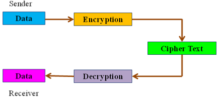
Digital data is protected using cryptography. Changing plaintext into illegible text and conversely is mention to as cryptosystem. It is an approach of transferring and saving data in a particular way so that just those who are meant to access and analyze it may do so. It is focuses on converting data into formats that can't be understood by unauthorized users. It's a message. The fact that it was encrypted simultaneously with the letters changing into other characters shows how basic the encryption algorithm was. see the Figure 1. The main cryptography principles are Data Confidentiality, Data Integrity, Authentication and Non-repudiation in modern day.
Figure 1. Cryptography process
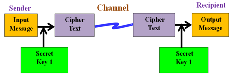
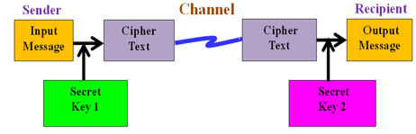
The fundamental elements of a cryptosystem include plaintext, which is the information that must be kept secure. The encryption algorithm is a mathematical process that takes plaintext as input and produces ciphertext, the encrypted or unintelligible counterpart to plaintext. Cryptography is divided into three main categories: secret key (symmetric key) encryption, public key (asymmetric key) encryption, and hash functions. In Symmetric Key Encryption, the same secret key, referred to as 'secret key 1' in Figure 2, is used for both encryption and decryption. In contrast, Asymmetric Key Encryption uses different keys for encryption and decryption; 'secret key 1' for encryption and 'secret key 2' for decryption, as shown in Figure 3.
Figure 2. Symmetric key encryption
Figure 3. Asymmetric key encryption
Messages can be securely encrypted and decrypted utilizing asymmetric cryptography, referred to as public key cryptography, effectively prevents them towards unauthorized access and utilization. A public key and a private key that are linked jointly are utilized. A single key is used for both encryption and decryption in symmetric encryption, which speeds up the encryption process. Asymmetric encryption uses two separate keys, one of which is related to the other by a challenging mathematical process; hence the encryption process is slower when using this method. Network security authentication and digital signature applications: Date and time stamping, electronic currency, the encryption and decryption of email, encrypting WhatsApp, The encryption of Instagram, Identification with a SIM card.
AES is the most well-known and often used symmetric encryption method available today. It can be found at least six times faster than triple DES. A replacement was required while the key size of DES was inadequate. As processing power spiked it became considered vulnerable to an exhaustive key search assault. Triple Data Encryption Standard was supposed to solve this disadvantage, but it was proven to be sluggish. In both hardware and software, AES is a popular and approved encryption method. AES has not yet been the target of any actual attacks using cryptanalysis. Additionally, the AES contains built-in flexibility for key length, providing some "future-proofing" against advancements in the capability of exhaustive key searches. However, AES security is only guaranteed if it is deployed correctly and sufficient key management is used, just like DES. AES encryption is frequently used by departments of the federal government, non-governmental organizations, commercial businesses, and NGOs to protect sensitive data. The AES algorithm is extensively used in many different fields, such as file encryption, SSL/TLS, processor security, and wireless security. Symmetric key encryption is used in the proposed approach. the key created at the sender's side using the input and the cipher key. The receiving side also generates the same key between the cipher and output.
Teng et al. [1] enhanced the hardware used to implement the AES Advanced Encryption Standard's SubBytes and Inverse SubBytes operations. To achieve this, the SubBytes (and inverse SubBytes) transformation's S-Box (and inverse S-Box) building blocks are all optimized using the composite field arithmetic (CFA) method. To increase area effectiveness, an S-Box and inverse S-Box combo design is also suggested. An S-Box throughput of 5.79 Gbps, 10% greater than in the prior study, may be achieved on a Virtex CPU. The results of the ASIC implementation indicate that the proposed design can still attain the highest area efficiency. Efficiency is boosted over conventional methods by roughly 30% when using the TSMC 90nm technology.
Nandan and Gowrı Shankar Rao [2] implemented the inverse of the improved affine transform is the main objective in this case. The basic ZigBee S-Box approach and the Rijndael method are compared in terms of a variety of factors. This is due to the use of extra registers for the various stages. A little adjustment to the affine (and inverse affine) transforms can be made to get around SBox's time and power limitations. The proposed transformation technique reduces the processing time for AES SBox. The projected system is 39% more powerful than the existing one. It is a system that works well.
Equihua et al. [3] showed the Galois Field Multiplier, which has been determined that the operated, that is involved in the Mix-Columns (and Inverse Mix-Columns) transformations, is the most demanded in terms of processing performance and area consumption. The Mix-Columns and Inverse Mix-Columns transformations use an optimized Galois Field Multiplier, which is discussed because it is the operation that uses the most storage and computing resources. The suggested GF (28) multiplier was optimized by two because to the huge number of multiplications needed by this circuit, allowing us to create a Mix-Columns circuit that is exceptionally compact.
Ueno et al. [4] represented Critical components combined with fewer additional selectors utilizing Datapath's innovative operation reordering and register-re timing algorithms. By using logic synthesis and the Nand Gate 45nm open cell library, it was possible to compared the performance of the proposed and several standard data paths. The efficiency of our suggested architectures is improved by about 51-64%.
Jindal et al. [5] researched on Simulation of the Advanced Encryption Standard utilizing double 7th series capital to examine cost and performance contrasts. The secret key is one and the same. Programmes in the public, private, commercial, etc. spheres may use it without restriction. Up to this point, thorough investigation is being conducted to identify methods to strengthen the AES algorithm's security.
Chauhan and Sasamal [6] specified about Generated multiple Sbox for different rounds that is Sbox changes with respect to key and hence increased the security of cipher. They compare the avalanche impact of basic AES with our suggested algorithm and alter AES so that it employs dynamic Sbox, which is key dependent.
Davis et al. [7] presented by adding a new realization of the ShiftRows operation utilizing muxes, new power-efficient AES implementation is introduced. The average overall power consumption of AES was reduced by 13.5% and 10.6%, respectively, in simulations of these implementations employing 45nm and 90nm technology nodes.
Gaded and Deshpande [8] represented S-Box, which uses Composite Field arithmetic, significantly reduces the area relative to FPGA slices and the gate latency as well as the combinational path delay
Shashidhar et al. [9] researched on Pipeline design for AES algorithm to increase the Performance of Hardware. They suggested sequential AES architecture has a maximum throughput of 37.21Gbps and a maximum operating frequency of 291.68MHz. In the AES Hardware implementation, three modules are used: encryption, decryption, and FPGA.
Srilaya and Velampalli [10] customized with when compared to AES, DES has a higher throughput for both encryption and decryption. Based on the input size, a comparison analysis has been conducted utilizing performance evaluation metrics for each approach. Throughput, power, memory, and encryption/decryption time are all measured together with simulation time.
Researchers [11-13] customized about the area-throughput trade-off for an ASIC's implementation of the Advanced Encryption Standard (AES) was stated. Throughputs of 30 Gbits/s to 70 Gbits/s are achievable in a 0.18-/spl mu/m CMOS technology using loop unrolling and outer-round pipelining techniques. Additionally, by pipelining the composite field implementation of the AES algorithm's byte replacement phase, the area consumption is reduced by up to 35%.
Sklavo and Koufopavlou [14] implemented two architectures. The first, employed feedback logic to achieve a throughput of 259 Mbit/sec. Applications with limited covered area resources benefit from its effective performance. Using a pipelined method, the second design is enhanced for high-speed performance. 3.65 Gbit/sec is its maximum throughput rate.
Abdel-Hafeez et al. [15] implemented in terms of throughput rate and hardware area is ALTERA series FPGA. They ran simulations to show that the proposed AES has a throughput rate that is about 16% greater than the conventional AES pipeline layout while reduced the hardware footprint by 36%.
Lakshmi and Sreenivasulu [16] represented about AES is a symmetric encryption method that employs a private key. Key Expansion, PreRound Operation, AddRoundKey, SubBytes, ShiftRows, and MixColumn are some of the building blocks used in this encryption procedure. The AES Algorithm employs cryptographic secret keys with lengths of 128bits, 192bits, and 256bits for encryption and 128bits for decoding input data. they displayed a study of the AES encryption algorithm.
3.1 AES-256 encryption
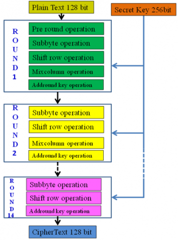
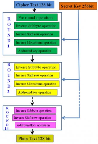
Advanced Encryption Standard (AES) has input data is 128bits, secret key is 128bits, 192bits and 256bits. Here using 256bit key algorithm. In 256bit key algorithm has total 14 rounds perform. There are 14 cycles for encryption and 14 rounds for AES decryption. It shows in Figures 4-5.
Substituting bytes (SubBytes): The design includes a fixed table (S-Box) that is hunted up in order to replace the 16 input bytes. The outcome is represented as a matrix with 4 rows and 4 columns. The 4 rows of the matrix are all shifted to the left. Any entries that 'fall off' are reinserted on the row's right side. During shift, the subsequent methods apply: The top row remains in place, The 2nd row has been moved 1(byte) position left, the 3rd row has been moved 2 spaces left, whereas the 4th row has been moved 3 spaces left. The end result is a new matrix with the same 16 bytes but with various locations.
Affine transformation [11]:
$\begin{array}{r}b^{\prime} i=b i \text { xor } b(i+4) \bmod 8 \text { xor } b(i+5) \bmod 8 \text { xor } b(i+6) \operatorname{mode} 8 \text { xor } b(i+7) \bmod 8 \text { xor ci }\end{array}$
for 0<=i<8 where ci is the ith bit of a byte c with the value 85 or 10000101 and bi is the ith bit of the byte. If a variable's prime value is b, it should be changed both here and elsewhere with the value shown on the right.
Figure 4. AES-256 encryption [16]
MixColumns: Each column of 4 bytes is now treated to a unique mathematical operation. In order to make use of this function, four bytes from one column need to be supplied, and four completely novel bytes should be output in its place. The most recent matrix has 16 more bytes and is a fresh one. This step does not appear in the final round, it should be highlighted.
AddRoundKey: The 16 bytes of the matrix, which are now regarded as 128 bits, are EX-ORed with the 128 bits of the round key. If this is the final attempt, the ciphertext will be generated. Otherwise, the outcome's 128 bits are transformed into 16 bytes, and the process is restarted. In the encryption's 1st round, 5 operations are performed, i.e., Pre-round, ShiftRow, AddRoundKey, SubBytes, and MixColumns. From the 2nd round to the 13th round, 4 operations are performed, i.e., SubBytes, ShiftRow, MixColumns, and AddRoundKey. For the 14th round, it performs only 3 operations, i.e., SubBytes, ShiftRow, and AddRoundKey operation (see Figure 4). Finally, the output is a 128-bit cipher key generated [1].
Depending on the key length, the State array is subjected to a round function 10, 12, or 14 times, with the final round differing somewhat from the early Nr-1 rounds. The cipher's definition is given in the pseudocode shown below. Each function handles the State separately: SubBytes(), ShiftRows(), MixColumns(), and AddRoundKey().
Encryption PseudoCode for the Cipher [11]:
Cipher(byte in[4*Nb], byte out[4*Nb], word w[Nb*(Nr+1)])
begin
byte state[4,Nb]
state = in
AddRoundKey(state, w[0, Nb-1])
for round = 1 step 1 to Nr–1
SubBytes(state)
ShiftRows(state)
MixColumns(state)
AddRoundKey(state, w[round*Nb, (round+1)*Nb-1])
end for
SubBytes(state)
ShiftRows(state)
AddRoundKey(state, w[Nr*Nb, (Nr+1)*Nb-1])
out = state
end
Where Nb: Number of Blocks
Nr: Number of Rounds
3.2 AES-256 decryption
AES-256 decryption has input is cipherkey 128bits, cipher key means combined of input data and secret key. Secret key is 128bits, 192bits and 256bits. Here using 256bit key algorithm. In 256bit key algorithm has total 14 rounds perform. For decryption has 14 rounds İt shows in Figure 5. The reversal of the encryption process is used in the decryption of an AES ciphertext. The four procedures are carried out each round in reverse sequence. Inverse SubByte replacement, Inverse Mixcolumn, Inverse Shiftrow, and Inverse Addroundkey are all examples of inverse operations. Despite having extremely close relationships, the encryption and decryption algorithms must be implemented independently since each round's sub-processes function backwards. In decryption 1st round perform 5 operations i.e., Preround, Inv shift row, addround key, Invsubbyte and Invmixcolumn. From 2nd round to 13th round perform 4 operations i.e., Invsubbyte, Invshiftrow, Invmixcolumn and addround key. For 14th round it perform 3 operations only i.e., Invsubbyte, Invshiftrow, Addroundkey operation see the Figure 5. Finally, the output is 128bits original data or input data generates.
An easy-to-use Inverse Cipher for the AES algorithm can be created by inverting the cipher transformations and then implementing them in reverse order. the various Inverse Cipher transformations InvShiftRows(), InvSubBytes(), InvMixColumns(), and AddRoundKey(). The array w[] includes the key schedule, and the pseudocode describing the Inverse Cipher is provided below.
Decryption PseudoCode for the InverseCipher [11]:
InvCipher(bytein[4*Nb],byteout[4*Nb],word w[Nb*(Nr+1)]) begin
byte state[4,Nb] state = in
AddRoundKey(state, w[Nr*Nb, (Nr+1)*Nb-1])
for round = Nr-1 step -1 downto 1
InvShiftRows(state)
InvSubBytes(state)
AddRoundKey(state, w[round*Nb, (round+1)*Nb-1])
InvMixColumns(state)
end for
InvShiftRows(state)
InvSubBytes(state)
AddRoundKey(state, w[0, Nb-1])
out = state
end
Figure 5. AES-256 decryption [16]
4.1 S-Box using logic gates
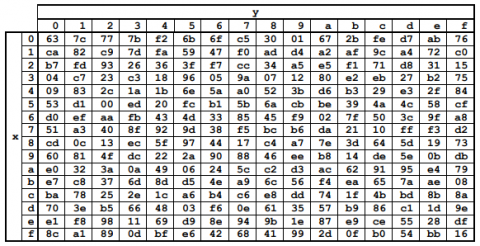
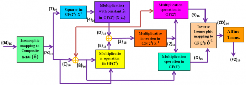
The Example for Computing the Sub Byte Operation with XOR Gates in S-Box is show in Figure 6(a), the dissemination of the data input of (04)16 into a composite field based Substitute Box. The precomputed values were formerly kept in a ROM-based lookup table, which was one of the most popular and simple implementations of the StandardBox for the SubByte operation (LUT). In this approach, the input byte would be connected to the ROM's address bus and all 256 values would be kept in a ROM. The multiplicative inversion of the supplied data is the first step. The four bit numbers outside of the logical blocks show the new values that are applied to the high and low nibbles. Since the results containing for GF(24) multiplication and multiplicative inverses are provided, the example can be completed by hand. Following the multiplicative inversion module's inverse isomorphic mapping operation, to create the S-Box Shown in Figure 6 (a). replacement value for the input, an affine transformation is applied to the multiplicative inverse of (CB)16. Finally, the output is (F2)16, which is consistent with the S-Box table given. Combinational logic(XOR Gate) is a more sophisticated method of implementing the S-Box, and this kind of S-Box has the benefit of having low space occupancy or less area occupied in the Virtex FPGA system [11, 12].
4.2 Isomorphic and inverse isomorphic mapping
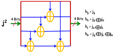
The logical XOR operation can be used to translate the matrix multiplication as shown in Figure 7. Below is a diagram of the matrices' logical form.
$\boldsymbol{\delta x j}=\left(\begin{array}{llllllll}1 & 0 & 1 & 0 & 0 & 0 & 0 & 0 \\ 1 & 1 & 0 & 1 & 1 & 1 & 1 & 0 \\ 1 & 0 & 1 & 0 & 1 & 1 & 0 & 0 \\ 1 & 0 & 1 & 0 & 1 & 1 & 1 & 0 \\ 1 & 1 & 0 & 0 & 0 & 1 & 1 & 0 \\ 1 & 0 & 0 & 1 & 1 & 1 & 1 & 0 \\ 0 & 1 & 0 & 1 & 0 & 0 & 1 & 0 \\ 0 & 1 & 0 & 0 & 0 & 0 & 1 & 1\end{array}\right) \mathbf{x}\left(\begin{array}{c}\mathrm{j}_7 \\ \mathrm{j}_6 \\ \mathrm{j}_5 \\ \mathrm{j}_4 \\ \mathrm{j}_3 \\ \mathrm{j}_2 \\ \mathrm{j}_1 \\ \mathrm{j}_0\end{array}\right)$
$\boldsymbol{\delta}^{-1} \mathbf{x}=\left(\begin{array}{cccccccc}1 & 0 & 1 & 0 & 0 & 0 & 0 & 0 \\ 1 & 1 & 0 & 1 & 1 & 1 & 1 & 0 \\ 1 & 0 & 1 & 0 & 1 & 1 & 0 & 0 \\ 1 & 0 & 1 & 0 & 1 & 1 & 1 & 0 \\ 1 & 1 & 0 & 0 & 0 & 1 & 1 & 0 \\ 1 & 0 & 0 & 1 & 1 & 1 & 1 & 0 \\ 0 & 1 & 0 & 1 & 0 & 0 & 1 & 0 \\ 0 & 1 & 0 & 0 & 0 & 0 & 1 & 1\end{array}\right) \mathbf{x}\left(\begin{array}{c}j_7 \\ j_6 \\ j_5 \\ j_4 \\ j_3 \\ j_2 \\ j_1 \\ j_0\end{array}\right)$
The above matrices simplified then becomes:
$\delta \mathbf{x j}=\left(\begin{array}{c}\mathrm{j}_7 \oplus \mathrm{j}_5 \\ \mathrm{j}_7 \oplus \mathrm{j}_6 \oplus \mathrm{j}_4 \oplus \mathrm{j}_3 \oplus \mathrm{j}_2 \oplus \mathrm{j}_1 \\ \mathrm{j}_7 \oplus \mathrm{j}_5 \oplus \mathrm{j}_3 \oplus \mathrm{j}_2 \\ \mathrm{j}_7 \oplus \mathrm{j}_5 \oplus \mathrm{j}_3 \oplus \mathrm{j}_2 \oplus \mathrm{j}_1 \\ \mathrm{j}_7 \oplus \mathrm{j}_6 \oplus \mathrm{j}_2 \oplus \mathrm{j}_1 \\ \mathrm{j}_7 \oplus \mathrm{j}_4 \oplus \mathrm{j}_3 \oplus \mathrm{j}_2 \oplus \mathrm{j}_1 \\ \mathrm{j}_6 \oplus \mathrm{j}_4 \oplus \mathrm{j}_1 \\ \mathrm{j}_6 \oplus \mathrm{j}_1 \oplus \mathrm{j}_0\end{array}\right)$
$\delta^{-1} x \mathrm{j}=\left(\begin{array}{c}\mathrm{j}_7 \oplus \mathrm{j}_6 \oplus \mathrm{j}_5 \oplus \mathrm{j}_1 \\ \mathrm{j}_6 \oplus \mathrm{j}_2 \\ \mathrm{j}_6 \oplus \mathrm{j}_5 \oplus \mathrm{j}_1 \\ \mathrm{j}_6 \oplus \mathrm{j}_5 \oplus \mathrm{j}_4 \oplus \mathrm{j}_2 \oplus \mathrm{j}_1 \\ \mathrm{j}_5 \oplus \mathrm{j}_4 \oplus \mathrm{j}_3 \oplus \mathrm{j}_2 \oplus \mathrm{j}_1 \\ \mathrm{j}_7 \oplus \mathrm{j}_4 \oplus \mathrm{j}_3 \oplus \mathrm{j}_2 \oplus \mathrm{j}_1 \\ \mathrm{j}_5 \oplus \mathrm{j}_4 \\ \mathrm{j}_6 \oplus \mathrm{j}_5 \oplus \mathrm{j}_4 \oplus \mathrm{j}_2 \oplus \mathrm{j}_0\end{array}\right)$
4.3 Addition of GF(24)
The basic bitwise XOR operation between two elements in a Galois Field corresponds to the addition of two elements.
Polynomial Form:
(p6+p4+p2+p+1)+(p7+p+1)=p7+p6+p4+p2
Binary Form:
(10101111) xor (01111001) = (11010110)
Hexadecimal Form:
(AF) xor (79) = (D6)
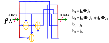
4.4 Squaring of GF(24)
Let b=j2 where b and j are elements of GF(24), represented by the binary number of {b3 b2 b1b0}2 and {j3 j2 j1 j0}2 respectively. It shows in Figure 6 (b) and Figure 7.
(a)
(b)
Figure 6. (a) S-Box values; (b) Diagram of squaring GF(24)
Figure 7. The example for computing the sub byte operation with logic gates in S-Box
Figure 8. Diagram of multiplying GF(24)
4.5 Multiplying with λ
λ is constant, let b=j λ, where b={b3 b2 b1 b0}2, j={j3 j2 j1 j0}2 and λ={1100}2 are elements of GF(24 ). It shows in Figures 7-8.
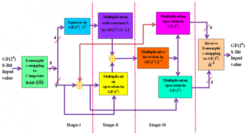
The concept of pipelining is based on sending water through a pipe continuously rather than waiting for it to empty. It therefore causes an increase in speed. Pipelining is a method of implementation where several instructions are executed simultaneously. There are many phases in the computer process. Each step simultaneously completes a portion of an instruction. Instructions enter at one end, go through the stages, and emerge at the other end of the pipe that connects them. Efficient systems include three pipeline stages for the byte substitution phase, as shown in Figure 9, the pipel registers for the three-stage S-Box are shown here in dotted lines. The input for Stage-I is an 8-bit value, GF(28), which is provided to the isomorphic mapping. One of the two resulting 4-bit values is given to the square in GF x2, and the remaining four bits are supplied to the ex-or block. Stage I's output serves as Stage II's input. It consists of multiplying by constants and x2, followed by multiplying by GF(24), and then xoring. Stage-II's output serves as Stage-III's input in Stage-III. It consists of multiplexing the inverse, multiplying two four-bit numbers, and isomorphic inversion obtained an 8 bit input value eventually. The main advantage of pipeline architecture reduces delay of system rather than increases speed of system.
Figure 9. The diagram of three pipeline stages S-Box
Figure 10. AES RTL schematic diagram
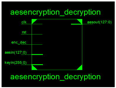
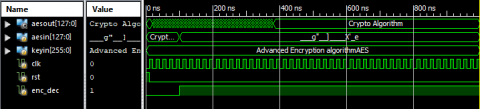
AES - 256 algorithms Encryption and Decryption schematic diagram is depicted in see Figure 10. Here taking clk, rst, enc_dec are input active low it acts as Encryption.
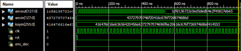
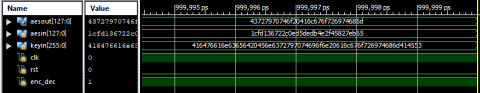
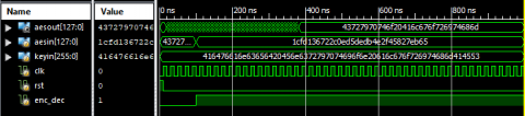
Example: If clk=0, rst=0, enc_dec=0 it operates as AES encryption. Encryption input is aesin=(43727970746f20416c676f726974686d)16, keyin =(416476616e63656420456e6372797074696f6e20616c676f726974686d414553)16. Finally got encryption output or cipher key bits are (1cfd136722c0ed5dedb4e2f45827eb65)16.
Later clk, rst, enc_dec are input active high it acts as Decryption. And aesin is 128 bit input, keyin is 256bit, aesout is 128bit.
Example: If clk=1, rst=1, enc_dec=1 it operates as AES decryption. Decryption input is cipher key=(1cfd136722c0ed5dedb4e2f45827eb65)16. keyin=(416476616e63656420456e6372797074696f6e20616c676f726974686d414553)16. Finally got decryption output or aesin bits are (43727970746f20416c676f726974686d)16.
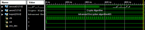
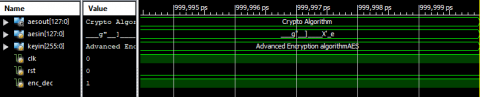
The Xilinx ISE design suite 14.7 tool was used to simulate each of the waveforms mentioned above once they had been incorporated in the Verilog testbench. Results of the AES-256 algorithm simulation for encryption and decryption Figures from Figures 11-16. Demonstrate hexadecimal and ASCII coding formats. When the inputs clk, rst, and enc_dec are active low, encryption is performed. Key size is 256 bits, and input is 128 bits. It produces an aesout, commonly known as a cipherkey 128 bit. Example: If clk=0, rst =0, enc_dec=0 it operate as AES encryption. Encryption input is aesin(ASCII Form)=“Crypto Algorithm”, keyin(ASCII Form) = “Advanced Encryption AlgorithmAES”.Finally got encryption output or cipherkey bits (Hexadecimal Form) are (1cfd136722c0ed5dedb4e2f45827eb65)16.
This cipherkey is used for decryption and outputs a 256-bit key that is identical to the encryption key. When clk, rst, and enc_dec are input and active high, decryption occurs. Later, it creates original data with a 128 bit encryption.
Example: If clk=1, rst=1, enc_dec=1 it operates as AES decryption. Decryption input is cipherkey (Hexadecimal Form)=(1cfd136722c0ed5dedb4e2f45827eb65)16. keyin=(ASCII Form)=“Advanced Encryption AlgorithmAES”. Finally got decryption output or aesin (ASCII Form)=“Crypto Algorithm”.
All inputs and outputs shown in above Table in form of HEX code and ASCII code forms (see Tables 1-2).
Figure 11. AES-256 Algorithm encryption (Hex Code)
Figure 12. AES-256 Algorithm encryption (ASCII Code)
Figure 13. AES-256 Algorithm decryption (Hex Code)
Figure 14. AES-256 Algorithm decryption (ASCII Code)
Table 1. AES-256 input, Cipher Key and output data
|
AES-256 Encryption Input/Output |
||
|
Input/Output |
In form of Hexadecimal Code |
Size |
|
aesin |
43727970746f20416c676f726974686d |
32 bytes |
|
keyin |
416476616e63656420456e6372797074696f6e20616c676f726974686d414553 |
64 Bytes |
|
aesout (Cipher Key) |
1cfd136722c0ed5dedb4e2f45827eb65 |
32 bytes |
|
Input/Output |
In form of ASCII Code |
Size |
|
aesin |
Crypto Algorithm |
16 bytes |
|
keyin |
Advanced Encryption Algorithm AES |
32 bytes |
|
aesout (Cipher Key) |
1cfd136722c0ed5dedb4e2f45827eb65 (Hex Code) |
32 bytes |
|
AES-256 Decryption Input/Output |
||
|
Input/Output |
In form of Hexadecimal Code |
Size |
|
aesin (Cipher Key) |
1cfd136722c0ed5dedb4e2f45827eb65 |
32 bytes |
|
keyin |
416476616e63656420456e6372797074696f6e20616c676f726974686d414553 |
64 Bytes |
|
Aesout |
43727970746f20416c676f726974686d |
32 bytes |
|
Input/Output |
In form of ASCII Code |
Size |
|
aesin (Cipher Key) |
1cfd136722c0ed5dedb4e2f45827eb65 (Hex Code) |
32 bytes |
|
keyin |
Advanced Encryption Algorithm AES |
32 bytes |
|
Aesout |
Crypto Algorithm |
16 bytes |
Table 2. AES input, Cıpher Key and output data size format
|
I/O Data Size format |
AES Input |
Key |
Cipher Key |
AES Output |
|
Binary Form |
128 bits |
256 bits |
128 bits |
128 bits |
|
Hexadecimal Form |
32 bytes |
64 bytes |
32 bytes |
32 bytes |
|
ASCII Form |
16 bytes |
32 bytes |
16 bytes |
16 bytes |
Figure 15. AES-256 Algorithm encryption and decryption (Hex Code)
Figure 16. AES-256 Algorithm encryption and decryption (ASCII Code)
8.1 Comparison of synthesis results of LUT based AES-256 with AES-256 using logic gates in terms of size or area
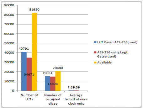
The FPGA device was used and synthesized on the evaluation platform Virtex-5 ML510. Following the synthesis of location and route, three parameter modifications occur, as represented by red colour stars in Table 3 and green colour stars in Table 3. The parameters are as follows: i) the number of LUTs, ii) the number of occupied slices, and iii) the average fanout of non-clock nets. These parameters reduced in Table 3, because this is using logic gate using for AES- 256 algorithm. So reduces above parameters that means area reduced AES-256 using Logic Gates than LUT based AES-256 and the chart representation as shown in Figure 17.
Table 3. Comparison between AES-256 logic gates Galois field approach vs utilizing LUTs in terms of size or area
|
Slice Logic Utilization |
Using LUTs |
Using Logic Gates |
|
Number of Slice LUTs |
40,791 |
34,671 |
|
Number of Occupied Slices |
15,034 |
14,808 |
|
Number of LUT Flipflop Pair Used |
40,791 |
34671 |
|
Number of IOBs |
513 |
513 |
|
Average Fanout of Non-Clock Nets |
7.69 |
5.59 |
|
Peak Memory Usage |
5157 MB |
5171 MB |
Figure 17. Chart representation of comparing parameters of LUT and Logic Gates using AES-256
Comparison of AES-256 using LUTs (Existing Methodology) with using Logic gates Galois field approach (Proposed Methodology) shows in Table 3. AES using logic gates Galois field approach is reduced area comparing Using LUT. And also it shows Figure 17 in graphical diagram format i.e. chart representation. In Chart, Blue color represents LUT Based Aes-256 utilization; Red color indicates AES -256 Using Logic Gates for Galois field approach utilization. Yellow color specifies available in FPGA device.
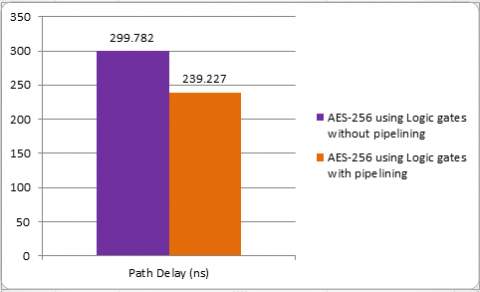
8.2 With and without pipelined logic gates using for AES-256 in terms of delay
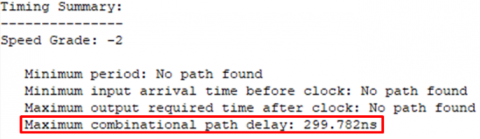
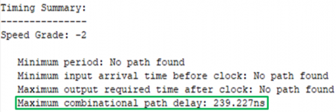
The FPGA Device used and synthesis with Virtex -5 ML510 Evolution platform. After synthesis of place and route then generate timing report. In timing summary path delay generates. The latency for AES-256 utilizing logic gates without pipelining is 299.782ns. It represents red colour in Figure 18. Delay high means speed also high. For reduce delay using AES-256 using Logic gates with three stage pipelining. Used pipelining the path Delay is 239.227ns it represents green colour in Figure 19. This system reduced path delay is 60.555ns. So this system performs fast compared to without pipeline. Delay Reduced and speed increased AES- 256 using Gates with pipeline than AES- 256 using Gates without pipeline. The chart representation shown in Figure 20. Comparison of path delay AES-256 using Logic gates without pipelining and Logic gates with Three stage pipelining shows in Table 4.
Figure 18. AES-256 using Logic gates without pipelining
Figure 19. AES-256 using Logic gates with pipelining
Table 4. Comparison of path delay AES-256 using Logic gates without and with Logic gates with pipelining
|
Timing Summary |
Logic Gates Without Pipelining |
Logic Gates with Three Stage Pipelining |
|
Path Delay (ns) |
299.782 |
239.227 |
Figure 20. Chart representation of comparing path delay of AES-256 using logic gates with and without pipelining
This paper represented Area or size efficient of S-Box AES-256 using Logic Gates Galois Field approach than S-Box LUT. Here analyzed and compared AES Logic gates approach reduced area and it occupies less space in Virtex FPGA chip in terms of number of slices LUTs are 6120, slice registers are 226, flip flops are 6120, and bonded IOB are 513 when compared to the LUT. Unwanted delays in this design are reduced because of the removal of LUTs, and a Three Stage pipelining structure is added to increase the performance of the AES algorithm. AES Logic gates three stage pipeline approach reduced delay up to 60.55ns when compared to Logic gates without pipeline approach. The proposed approach simulated and synthesized with Virtex-5 ML510 Evolution platform FPGA device along with design in Verilog code in XILINX 14.7 Software. In future work can add or combined hash algorithm with AES for better performance.
[1] Teng, Y.T., Chin, W.L., Chang, D.K., Chen, P.Y., Chen, P.W. (2021). VLSI architecture of S-Box with high area efficiency based on composite field arithmetic. IEEE Access, 10: 2721-2728. http://doi.org/10.1109/ACCESS.2021.3139040
[2] Nandan, V., Gowri Shankar Rao, R. (2022). Low-power and area‐efficient design of AES S-Box using enhanced transformation method for security application. International Journal of Communication Systems, 35(2): e4308. http://doi.org/10.1002/dac.4308
[3] Equihua, C., Anides, E., García, J.L., Vázquez, E., Sánchez, G., Avalos, J.G., Sánchez, G. (2021). A low-cost and highly compact FPGA-based encryption/decryption architecture for AES algorithm. IEEE Latin America Transactions, 19(9): 1443-1450. http://doi.org/10.1109/TLA.2021.9468436
[4] Ueno, R., Morioka, S., Miura, N., Matsuda, K., Nagata, M., Bhasin, S., Homma, N. (2019). High throughput/gate AES hardware architectures based on datapath compression. IEEE Transactions on Computers, 69(4): 534-548. http://doi.org/10.1109/TC.2019.2957355
[5] Jindal, P., Kaushik, A., Kumar, K. (2020). Design and implementation of advanced encryption standard algorithm on 7th series field programmable gate array. In 2020 7th International Conference on Smart Structures and Systems (ICSSS), Chennai, India, pp. 1-3. http://doi.org/10.1109/ICSSS49621.2020.9202114
[6] Chauhan, Y.S., Sasamal, T.N. (2019). Enhancing security of AES using key dependent dynamic Sbox. In 2019 International Conference on Communication and Electronics Systems (ICCES), Coimbatore, India, pp. 468-473. http://doi.org/10.1109/ICCES45898.2019.9002543
[7] Davis, C., Muthineni, A., John, E. (2019). Low-power advanced encryption standard for implantable cardiac devices. In 2019 IEEE 62nd International Midwest Symposium on Circuits and Systems (MWSCAS), Dallas, TX, USA, pp. 41-44. http://doi.org/10.1109/MWSCAS.2019.8884946
[8] Gaded, S.V., Deshpande, A. (2019). Composite field arithematic based s-box for aes algorithm. In 2019 3rd International Conference on Electronics, Communication and Aerospace Technology (ICECA), Coimbatore, India, pp. 1209-1213. http://doi.org/10.1109/ICECA.2019.8821862
[9] Shashidhar, R., Mahalingaswamy, A.M., Kumar, P., Roopa, M. (2018). Design of high speed AES system for efficient data encryption and decryption system using FPGA. In 2018 International Conference on Electrical, Electronics, Communication, Computer, and Optimization Techniques (ICEECCOT), Msyuru, India, pp. 1279-1282. http://doi.org/10.1109/ICEECCOT43722.2018.9001535
[10] Srilaya, S., Velampalli, S. (2018). Performance evaluation for des and AES algorithms-An comprehensive overview. In 2018 3rd IEEE International Conference on Recent Trends in Electronics, Information & Communication Technology (RTEICT), Bangalore, India, pp. 1264-1270. http://doi.org/10.1109/RTEICT42901.2018.9012536
[11] FIPS 197. (2001). Advanced Encryption Standard (AES). November 2.
[12] Biasizzo, M.M.F.N.A., Mali, M., Novak, F. (2005). Hardware implementation of AES algorithm. Journal of Electrical Engineering, 56(9-10): 265-269.
[13] Hodjat, A., Verbauwhede, I. (2006). Area-throughput trade-offs for fully pipelined 30 to 70 Gbits/s AES processors. IEEE Transactions on Computers, 55(4): 366-372. http://doi.org/ 10.1109/TC.2006.49
[14] Sklavos, N., Koufopavlou, O. (2002). Architectures and VLSI implementations of the AES-proposal Rijndael. IEEE Transactions on Computers, 51(12): 1454-1459. http://doi.org/ 10.1109/TC.2002.1146712
[15] Abdel-Hafeez, S., Sawalmeh, A., Bataineh, S. (2007). High performance AES design using pipelining structure over GF ((24)2). In 2007 IEEE International Conference on Signal Processing and Communications, Dubai, United Arab Emirates, pp. 716-719. http://doi.org/ 10.1109/ICSPC.2007.4728419
[16] Lakshmi, K.J., Sreenivasulu, G. (2021). A review on FPGA based design of advanced encryption standard (AES) cryptography secure algorithm. i-Manager's Journal on Communication Engineering and Systems, 10(1): 30. https://doi.org/10.26634/jcs.10.1.18378