Kanchan S. Tiwari*![]() | Rekha S. Kadam
| Rekha S. Kadam![]() | Manisha A. Dudhedia
| Manisha A. Dudhedia![]() | Jayshree R. Pansare
| Jayshree R. Pansare![]() | Shilpa P. Khedkar
| Shilpa P. Khedkar![]() | Shravan H. Gawande
| Shravan H. Gawande![]()
© 2024 The authors. This article is published by IIETA and is licensed under the CC BY 4.0 license (http://creativecommons.org/licenses/by/4.0/).
OPEN ACCESS
In recent years, reversible logic gates have garnered significant interest because of their potential to decrease energy consumption and meet the growing need for low-power computing systems. Unlike conventional logic gates, reversible logic gates ensure that no information loss happens during computation, allowing for the reversal of the entire computation process. This unique characteristic opens up new avenues for developing energy-efficient digital circuits. This review paper serves as a vital contribution to the field by addressing a noticeable gap in the existing literature regarding reversible logic gates. The study not only comprehensively analyzes the array of reversible logic gates available but also underscores their practical applications and significance. It encompasses a wide variety of reversible logic gates, including Toffoli gates, Fredkin gates, and newer innovations. It is found that Toffoli gates outperformed in terms of gate count and quantum cost reduction, making them a preferred choice for quantum circuit optimization. Additionally, Fredkin gates showed exceptional performance in specific applications, like data swapping and quantum state control. The digital circuits like adders, multiplexers, ALU etc. are successfully designed using reversible gates like HNG, DKG etc. The significant gap this study fills lies in the need for a consolidated and in-depth analysis of the state-of-the-art reversible logic gates and their real-world utility. While prior research has discussed these gates individually, this paper takes a novel approach by offering a holistic assessment of their performance, quantum cost, gate count, and practical applications, thereby presenting a comprehensive resource for researchers, engineers, and designers in the field. This innovative contribution plays a pivotal role in shaping the progress of energy-efficient and quantum computing systems as well as in optimizing VLSI chip designs for various applications, with a particular emphasis on enhancing cryptographic and data processing capabilities. The findings of this review aim to stimulate further research and development in reversible computing, contributing to the advancement of energy-efficient and information-preserving computing systems.
reversible logic gates, Toffoli gate, Fredkin gate, power dissipation, quantum computing, quantum cost, reversible logic application, low power design, cryptography
Gordon Moore, one of the co-founders of Intel Corporation, made a famous prediction in 1965 that came to be known as Moore's Law [1]. He noted that the doubling of transistors on a silicon chip occurred at approximately two-year intervals, resulting in a notable augmentation of computing capabilities. The reduction in feature size has led to several implementation and operational difficulties. It is difficult for CMOS technology to continue to the required level of growth. Since the power consumption of CMOS circuit increases with clock frequency and the frequency determines the computation speed and performance, an increase in performance also increases the power consumption [2]. The challenge is the unsustainable relationship between power consumption versus performance.
The Landauer principles [3, 4] states that the removal of one bit of information during an irreversible computation necessitates a minimum energy dissipation of approximately kT ln(2), where 'k' represents the Boltzmann constant, and 'T' denotes the temperature in Kelvin. This principle implies that for each bit erased, a minimum of kT ln(2) joules of energy must be dissipated in the form of heat. In 1973, Charles H. Bennett published a groundbreaking study titled "Logical Reversibility of Computation," which laid the foundation for the field of reversible computing [5]. Bennett's study [6] explored the theoretical underpinnings and implications of reversible computation, focusing on its fundamental connection to thermodynamics and information theory. In the study, Bennett demonstrated that logical reversibility is a key concept in achieving energy-efficient computation. The concept of reversible computation, which he introduced, involves a scenario in which every computational step is entirely invertible. This feature permits the retrieval of the initial state from the final state with no information loss. Bennett's work showed that reversible computation has significant implications for reducing energy dissipation in computing systems.
Reversible logic, also known as reversible computing or reversible gates, is a computing paradigm that focuses on designing logic circuits or systems that can perform computations without losing information [7]. Unlike conventional logic gates, which are irreversible that discard or overwrite bits, and can result in information loss through dissipative processes like heat generation, reversible logic gates guarantee the individual recovery of all input information from the output, establishing a direct one-to-one relationship between the input and output. This property enables the computation to be reversible, allowing the system to be able to "undo" operations and revert back to the original state. This preservation of information allows for energy conservation since no energy is dissipated as heat due to information loss. The major advantages which one can gain by using reversible logic circuits are:
Energy efficiency: Reversible logic gates are engineered with the goal of reducing energy dissipation [8] while preserving all information throughout computation. As the feature size decreases, power density and leakage currents become more significant challenges. By adopting reversible logic, which inherently aims to conserve energy, it is possible to reduce power consumption and mitigate some of the energy-related challenges associated with scaling [9].
Reduced gate count: Reversible logic gates typically have fewer gates compared to their irreversible counterparts for achieving the same functionality. This reduction in gate count can be advantageous in VLSI chip design, as it helps to minimize the increasing complexity and fabrication challenges caused by shrinking feature sizes. Fewer gates lead to simpler designs, which can enhance manufacturability, yield, and overall circuit performance.
Signal integrity: Reversible logic gates often exhibit lower fan-out and reduced signal propagation delays compared to irreversible gates [10]. These characteristics can help maintain better signal integrity and alleviate some of the challenges related to interconnect delays, crosstalk, and power supply noise. By reducing the impact of signal integrity issues, reversible logic can contribute to more reliable and efficient circuit operation.
Quantum computing considerations: Reversible logic gates have a vital role within the domain of quantum computing [11], which utilizes quantum bits (Qubits) [12-14] that must maintain coherence throughout computation. While reversible logic in classical VLSI chips does not directly address quantum computing challenges, the experience gained from reversible logic design techniques and circuit optimization approaches can be valuable for developing future quantum computing technologies.
Reversible logic along with process technology advancements, device engineering, circuit design methodologies, and manufacturing techniques offers potential benefits in terms of energy efficiency, gate count reduction, and signal integrity. Reversible logic has the potential to drastically reduce power consumption in computing systems, making it a promising approach for energy-efficient computing, especially in scenarios where power consumption is a critical factor, such as in quantum computing, nanotechnology, and low-power embedded systems [15]. Reversible logic gates, such as the Feynman gate, Fredkin gate, Toffoli gate, and Peres gate, Feynman double gate [16-18], have been developed as building blocks for reversible circuits. These gates have the property of being reversible, allowing computations to be performed with guaranteed information preservation. Research in the area of reversible logic encompasses various aspects, including circuit design, synthesis, optimization, fault tolerance, and applications. Researchers continue to explore and develop reversible logic design techniques, algorithms, and architectures to harness its benefits in various applications. Currently, reversible logic is used to implement various combinational and sequential circuits like ALU, counters, encoders, flip flops, fault checkers, etc. [19]. Some research directions and recent advancements in the field are as follows:
Circuit design and synthesis: Researchers are developing efficient methodologies for designing and synthesizing reversible circuits [20-28]. This involves the exploration of novel gate libraries, reversible gates, and building blocks that can perform computations without any loss of information.
Optimization techniques: Several optimization techniques are being explored to lessen the number of gates, garbage outputs, and quantum cost of reversible circuits [29-40]. This includes approaches like gate-level optimization, logic synthesis, gate swapping, and technology mapping.
Quantum reversible logic: Reversible logic plays a significant role in quantum computing [39]. Researchers are investigating reversible logic synthesis techniques tailored for quantum circuits. The objective is to minimize the quantum cost and improve the overall efficiency of quantum computations [41, 42].
Fault-tolerant reversible logic: Fault tolerance is crucial in any computing system. Researchers are studying fault-tolerant designs and fault diagnosis techniques for reversible logic circuits. Redundancy-based approaches, error detection and correction codes, and fault modeling are areas of active research in the area of reversible logic [43-46].
Reversible logic applications: Reversible logic has applications in various fields, including cryptography, image processing, data compression, quantum computing, and low-power computing [47-50]. Research focuses on developing efficient reversible algorithms and architectures for these applications.
Quantum computing and reversible logic: Reversible logic is deeply connected to quantum computing due to the reversible nature of quantum operations [51-56]. Research explores the relationship between reversible logic and quantum computing, including the development of reversible quantum gates and reversible circuit synthesis for quantum algorithms.
Reversible logic and energy efficiency: One of the key motivations behind reversible logic is energy efficiency [57]. Researchers investigate the impact of reversible logic in reducing power consumption, heat dissipation, and overall energy requirements in different computing paradigms, such as classical and quantum computing.
These are just a few research directions within the area of reversible logic. This field draws attention from all disciplines involving aspects of computer science, electrical engineering, quantum physics, and information theory. Ongoing research aims to improve the theoretical foundations, design methodologies, and practical implementation of reversible logic, with the goal of realizing energy-efficient computing systems. In this study, our primary objective is to comprehensively analyze the performance and applications of various reversible logic gates. Specifically, we aim to address the following aspects:
•The quantum cost and gate count associated with different reversible logic gates.
•Real-world applications and implications of these gates, with a particular focus on their relevance in quantum computing, energy-efficient computing, and VLSI chip design.
This paper is structured as follows: Section 2 provides an in-depth analysis of the basic parameters associated with various reversible logic gates. In Section 3, we explore all gates invented till date. Section 4 offers a comparative analysis of our findings and highlights the practical benefits and implications of our research along with its popular applications. Finally, in Section 5, we conclude by summarizing our work and underscoring its novelty and significance.
As defined in literature [58], there are several terminologies and parameters related to reversible logics. In this section, the terminologies are explained in detail:
Figure 1. Reversible logic gate
The reversible logic gate is a logic device having n inputs and n outputs as shown in Figure 1. The 'n' inputs are a combination of 'a' primary inputs and 'b' constant inputs (a+b=n), and similarly ‘n’ outputs on the output side, which are made up of 'x' primary outputs and 'y' garbage outputs such that x+y=n. The reversible circuit should be designed in such a way that it requires reversible logic gates, input constant, and garbage outputs minimum.
Constant inputs: These are fixed inputs provided to the reversible gate that do not change. They can be used to control the gate's behavior or enforce specific logic operations. They are essential for achieving specific computations, optimizing circuit performance, and enhancing the flexibility and programmability of reversible logic circuits.
Garbage outputs: In reversible computing, garbage outputs refer to the bits that do not contribute to the final output and are essentially discarded. Minimizing the number of garbage outputs is crucial in designing efficient reversible circuits. One has to preserve the following relation while designing a reversible circuit:
inputs+constant inputs=outputs+garbage outputs.
Fan-out: In reversible logic, the fan-out parameter refers to the maximum number of gates that can directly receive the output of a particular gate without any additional measures, such as auxiliary gates or circuit modifications; while maintaining reversibility and the direct correspondence between input and output states remains a one-to-one relationship. Unlike classical logic gates, achieving direct fan-out in reversible logic is challenging due to the requirement of preserving information and reversibility. The reversible gates used in the circuit design should ensure that each input state maps to a unique output state, making it difficult to directly connect multiple gates to a single output without violating this property. Fan-out, the number of times an output is used as an input in reversible logic circuits, impacts performance and design. High fan-out can increase gate complexity because gates with multiple inputs (controlled by the fan-out) may require additional resources to maintain reversibility; increase propagation delay as when an output is connected to multiple inputs of other gates (high fan-out), it can slow down the circuit's overall operation because the signal must fan out to multiple destinations, potentially causing delays; increase quantum cost as more gates may be needed to achieve the same functionality and the need to manage garbage outputs. Designers must balance fan-out to optimize circuit efficiency while preserving reversibility.
Flexibility: Flexibility shows the universality of reversible logic gates. Flexibility in reversible logic gates refers to their ability to perform a wide range of computational tasks while still adhering to the principles of reversibility. This includes not just performing basic logical operations but also more complex transformations and computations. A flexible reversible logic gate should be capable of emulating any other reversible or irreversible gate or circuit. The Toffoli gate, for example, is a commonly used universal reversible gate that can emulate various other gates and functions. To achieve reversibility, we need minimal garbage output, minimal delay, and no feedback/loops.
Delay: The delay parameter refers to the time required for a reversible gate or circuit to propagate its input changes to the output. It represents the time delay experienced by the signals passing through the gate or circuit. The definition relies on two underlying premises: (i) Each gate carries out the computation within a single unit of time, and (ii) All inputs to the circuit are accessible prior to the commencement of computation.
Gate count: It is measure of the total number of reversible gates used in a circuit. It indicates the complexity of the circuit and affects factors such as circuit size, power consumption, and delay.
Hardware complexity: Each reversible gate performs a specific logic operation, such as AND, OR, EX-OR, or NOT. The gate's functionality is defined by the way it transforms the input signals into output signals. For example, the Toffoli gate performs a controlled NOT operation, while the Fredkin gate swaps the values of two input bits based on a control bit. The hardware complexity determines the number of logical operations performed in the circuit, such as AND, OR, EX-OR. In the realm of reversible logic gates, hardware complexity can significantly impact:
•Performance: Complex gates can slow down the circuit operation.
•Quantum cost: High complexity can raise the quantum cost in quantum computing.
•Gate count: More complex gates demand more resources, affecting cost and scalability.
•Reliability: Complexity can increase error probabilities affecting reliability.
•Resource efficiency: Simplifying gates is crucial for efficient resource utilization.
•Ease of programming: Simpler gates are easier to program and maintain, thereby reducing development costs.
Reversibility degree: The reversibility degree measures the extent to which a circuit or gate is reversible. It refers to the ratio of the number of input combinations that yield unique output combinations to the total number of possible input combinations.
Reversibility Degree=(Number of Unique Output Combinations)/(Total Number of Possible Input Combinations)
For example, as for a 2×2 reversible Peres gate, there will be 4 unique input and output combinations, hence its reversibility degree is 100%.
Quantum cost: Quantum cost measures the computational resources required to implement a reversible logic gate. It is often quantified in terms of the number of two qubit gates or elementary gates (such as NOT, CNOT, and Toffoli gates) needed to construct a given reversible gate. Quantum cost optimization is an important consideration in reversible logic design, as minimizing the quantum cost leads to more efficient and less resource-intensive implementations. Various techniques and algorithms, such as synthesis and optimization tools, can be employed to reduce the quantum cost of reversible logic circuits. Strategies for optimization include gate count reduction, gate synthesis, compiler optimization, heuristic methods, and the use of error correction techniques. Ongoing research and libraries of pre-optimized gates contribute to improving efficiency in quantum computation.
In summary, each parameter impacts the efficiency and effectiveness of reversible logic gates by influencing factors like speed, resource consumption, reliability, ease of design and maintenance, and suitability for various applications. Reducing gate count, fan-out, hardware complexity, garbage output, quantum cost, and resource demands all lead to more efficient and effective circuits.
In the next section, the discussion on reversible gates available in the literature till now is presented.
The methodology for this research paper involves a comprehensive and systematic analysis of various reversible logic gates and their applications mentioned in research papers. The selection of reversible logic gates for analysis was based on several key criteria, including their historical significance, prevalence in modern applications, and representation of different gate types. The chosen gates represent a spectrum of gate functionalities, including Toffoli gates, Fredkin gates, and newer innovations, allowing for a comprehensive analysis of the field. The applications of reversible logic gates were analyzed through a multi-faceted approach. This involved studying their use in quantum computing, energy-efficient computing systems, and VLSI chip design. A comparative analysis was conducted to assess their performance in these domains. Real-world implementations and case studies were also examined to understand the practical implications. The upcoming subsection introduces reversible gates categorized by the dimensions of their inputs and outputs. According to the latest developments in the field, the largest input and output size achievable stands at 6.
3.1 2×2 reversible logic gates
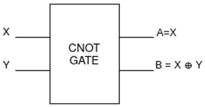
3.1.1 CNOT / FEYNMAN gate
The CNOT gate, short for Controlled-NOT gate [59], is a fundamental reversible logic gate (Figure 2) commonly used in reversible computing and quantum computing. This gate is a 2×2 gate having two inputs clubbed together in the vector form as In={X, Y} and similarly outputs as Out={X, X$\oplus$Y}. It operates on two input bits, a control bit (X) and a target bit (Y), and produces two output bits, maintaining the same control bit and possibly flipping the target bit.
The behavior of the CNOT gate can be summarized as follows:
If the control bit (X) is 0, the output remains the same as the input: (X, Y) → (X, Y).
If the control bit (X) is 1, the target bit (Y) is flipped: (X, Y) → (X, NOT(Y)).
In other words, the CNOT gate copies the value of the control bit to the target bit when the control bit is 1, and leaves the target bit unchanged when the control bit is 0. The CNOT gate is a fundamental component in quantum error correction codes, such as the surface code. The quantum cost is 1. It is used to propagate errors and perform syndrome measurements, allowing the detection and correction of errors that occur during quantum computations. Feynman gate is used for duplication of outputs.
Figure 2. CNOT gate
3.2 3×3 reversible logic gates
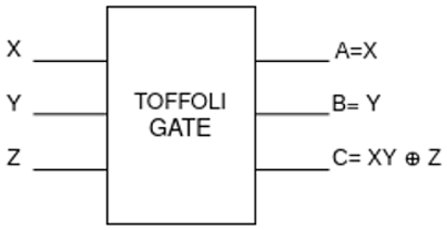
3.2.1 TOFFOLI gate
The Toffoli gate (Figure 3), also known as the Controlled-Controlled-Not (CCNOT) gate, is a fundamental gate in quantum computing. It is named after the physicist Tommaso Toffoli, who first introduced it in 1980. This gate is characterized by 3 inputs and 3 outputs as its 3×3 gate. The inputs are clubbed together to represent in the form of a vector as In={X, Y, Z} and the output as Out={X, Y, XY$\oplus$Z}. The last bit is the target bit, the rest are control bits, when the control bit is 1, the target bit is inverted. The quantum cost is 5. Toffoli gate can be used to realize any function, hence it is known as a universal reversible gate [60]. It is used for quantum error correction applications [61].
Figure 3. TOFFOLI gate
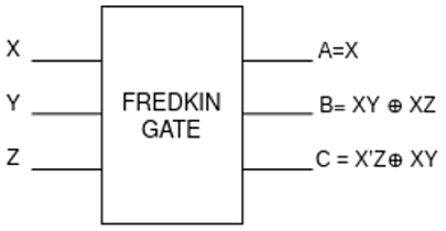
3.2.2 FREDKIN gate
The Fredkin gate as shown in Figure 4, also known as the Controlled-Swap (CSWAP) gate or the Controlled-Permutation gate, is a reversible three-Qubits gate named after the computer scientist Edward Fredkin who invented it in 1982 [17]. The set of input are In={X, Y, Z} and the outputs are Out={X, XY$\oplus$XZ, X’Z$\oplus$XY}. The input X is mapped directly to the output A. If X=0, Y is mapped to B, Z is mapped to C. If X=1, a swap operation is performed and Y is mapped to C and Z is mapped to B. Therefore, it is also known as a Controlled SWAP gate. The quantum cost is 5. Fredkin gate is used to preserve parity [62].
Figure 4. FREDKIN gate
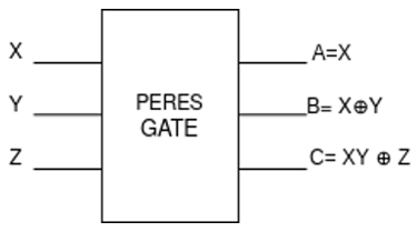
3.2.3 PERES gate
The PERES gate (Figure 5), also known as the Peres-Horodecki gate, is a two-qubit gate named after Asher Peres and Michał Horodecki, who contributed to its study in 1996 [16]. It is an entanglement detection gate that determines whether two Qubits are entangled or separable. The input is represented as In={X, Y, Z} and the output is represented as Out={X, X$\oplus$Y, XY$\oplus$Z}. The quantum cost is 4. TRG gate is used for the implementation of a full subtractor. Peres gate can be used to realize functions like NOT, AND, NAND, XOR [61].
Figure 5. PERES gate
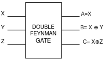
3.2.4 Double Feynman gate
The input is represented as In={X, Y, Z} and the output is represented as Out={X, X$\oplus$Y, X$\oplus$Z}. The quantum cost is 2. Double Feynman gate shown in Figure 6 is a parity preserving gate [63, 64].
Figure 6. DOUBLE FEYNMAN gate
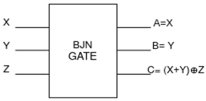
3.2.5 BJN gate
In Figure 7, BJN gate is shown. The input is represented as In={X, Y, Z} and the output is expressed as Out={X, Y,(X+Y)$\oplus$Z}. The quantum cost is 5 [62].
Figure 7. BJN gate
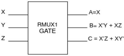
3.2.6 RMUX 1 gate
The input is represented as In={X, Y, Z} and the output is represented as Out={X, X’Y+XZ, X’Z+XY'}. The quantum cost is 4. RMUX1 gate as shown in Figure 8 works as a 2:1 MUX, where X is the select line and Y&Z are the two inputs [65].
Figure 8. RMUX1 gate
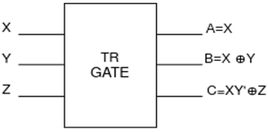
3.2.7 TRG gate
The block diagram of TRG gate is shown in Figure 9. The input is represented as In={X, Y, Z} and the output is represented as Out={X, X$\oplus$Y, XY’$\oplus$Z'}. The quantum cost is 4. TRG gate is used for the implementation of a full subtractor circuit [65].
Figure 9. TRG gate
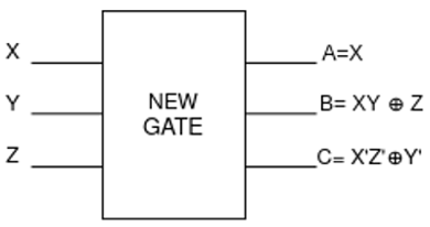
3.2.8 NEW gate
The block diagram of NEW gate is shown in Figure 10. The input is represented as In={X, Y, Z} and the output is represented as Out={X, XY$\oplus$Z, X’Z’$\oplus$Y’} [65].
Figure 10. NEW gate
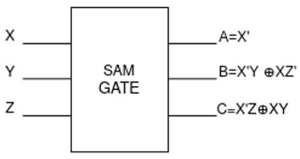
3.2.9 SAM gate
The input vector In={X, Y, Z} and the output vector Out={X’, X’Y$\oplus$XZ’, X’Z$\oplus$XY} for the SAM Gate is shown in Figure 11 [64].
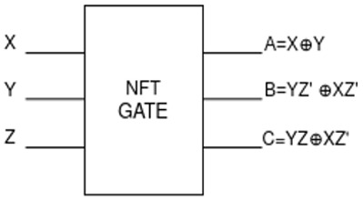
3.2.10 NFT gate
New fault tolerant gate is a gate for parity preserving. Its block diagram is shown in Figure 12. The input is represented as In={X, Y, Z} and the output is represented as Out={X$\oplus$Y, YZ’$\oplus$XZ’, YZ$\oplus$XZ’} [63].
Figure 11. SAM gate
Figure 12. NFT gate
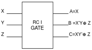
3.2.11 RC-I gate
RC-I gate is a single bit comparator circuit. Figure 13 displays its block diagram. The input is represented as In={X, Y, Z} and the output is represented as Out={X, X’Y$\oplus$Z, XY’$\oplus$Z}. It compares X and Y [66].
Figure 13. RC I gate
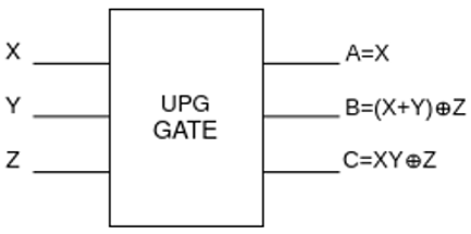
3.2.12 UPG gate
Universal programmable gate (UPG) as the name implies can be used to implement logical functions like NAND, AND OR, and NOR. The input is represented as In={X, Y, Z} and the output is represented as Out={X, (X+Y)$\oplus$Z, XY$\oplus$Z}. It can perform logical operations at low quantum cost. Its block diagram is shown in Figure 14 [65].
Figure 14. UPG Gate
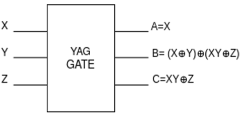
3.2.13. YAG gate
The input is represented as In={X, Y, Z} and the output is represented as Out={X, (X$\oplus$Y)$\oplus$(XY$\oplus$Z), XY$\oplus$Z}.
YAG is used to realize AND and OR functions. Its block diagram is shown in Figure 15 [67].
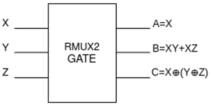
3.2.14 RMUX2 gate
The input is represented as In={X, Y, Z} and the output is represented as Out={X, XYv+XZ, X$\oplus$(Y$\oplus$Z)}. Its quantum cost is 4. In this gate, X is the select line, the gate gives the multiplexed output of Y and Z Its block diagram is shown in Figure 16 [65].
Figure 15. YAG gate
Figure 16. RMUX2 gate
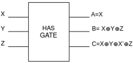
3.2.15 HAS gate
Half Adder Subtraction gate has quantum cost 5. The input is represented as In={X,Y,Z} and the output is represented as Out={X, X$\oplus$Y$\oplus$Z, X$\oplus$Y$\oplus$X’$\oplus$Z}. HAS gate is used to implement BCD adder, carry skip BCD adder circuit, half adder, and full subtractor [68]. Its block diagram is shown in Figure 17.
Figure 17. HAS gate
3.3 4×4 reversible logic gates
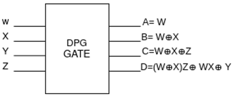
3.3.1 Double Peres gate
Double Peres gate is used to implement the full adder [69]. Figure 18 represents its block diagram. The input is represented as In={W, X, Y, Z} and the output is represented as Out={W, W$\oplus$X, W$\oplus$X$\oplus$Z, (W$\oplus$X)Z$\oplus$WX$\oplus$Y}. The quantum cost is 6.
Figure 18. DPG gate
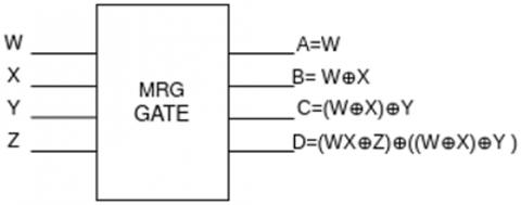
3.3.2 MRG gate
Marrison-Ranganathan gate (MRG) is a programmable gate. The input is represented as In={W, X, Y, Z} and the output is represented as Out ={W, W$\oplus$X, (W$\oplus$X)$\oplus$Y, (WX$\oplus$Z)$\oplus$(W$\oplus$X)$\oplus$Y}. The quantum cost is 6. The 4 operations that MRG gate can perform are OR, NOR, XNOR, and XOR. Its block diagram is shown in Figure 19 [70].
Figure 19. MRG gate
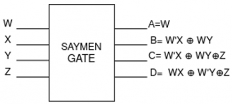
3.3.3 SAYEM gate
The input is represented as In={W, X, Y, Z} and the output is represented as Out={W, W’X$\oplus$WY, W’X$\oplus$WY$\oplus$Z, WX$\oplus$W’Y$\oplus$Z}. The Sayem gate is a versatile component that can be employed in the construction of reversible standard sequential circuits, including popular flip-flop designs such as the T flip-flop and D flip-flop, in conjunction with the Feynman gate. This combination of components allows for the creation of advanced sequential logic circuits with the unique property of reversibility. Its block diagram is shown in Figure 20 [60].
Figure 20. SAYME gate
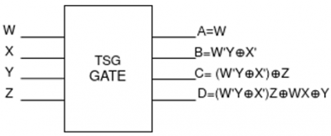
3.3.4 TSG gate
The input is represented as In={W, X, Y, Z} and the output is represented as Out={W, W’Y$\oplus$X’, (W’Y$\oplus$X’)$\oplus$Z, (W’Y$\oplus$X’)Z$\oplus$WX$\oplus$Y}. The TSG gate, in conjunction with the CNOT (Controlled-NOT) gate, serves as the fundamental building block for the implementation of a full adder. This powerful combination of gates enables the creation of a full adder circuit, a fundamental component in digital arithmetic. Its block diagram is shown in Figure 21 [71].
Figure 21. TSG gate
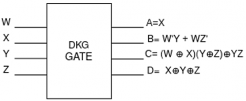
3.3.5 DKG gate
The input is represented as In={W, X, Y, Z} and the output is represented as Out={X, W’Y+WZ’, (W$\oplus$X)(Y$\oplus$Z)$\oplus$YZ, X$\oplus$Y$\oplus$Z}. DKG gates can singly work as either a full adder or a full subtractor. W is the control line, if W is set to 0, it will work as full adder, and if W is set to 1, it will work as full subtractor. Its block diagram is shown in Figure 22 [71, 72].
Figure 22. DKG gate
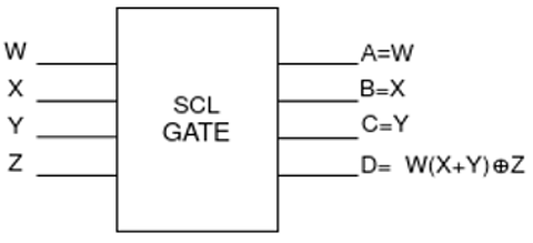
3.3.6 SCL gate
The input is represented as In={W, X, Y, Z} and the output is represented as Out={W, X, Y, W(X+Y)$\oplus$Z}. SCL gate is used to add 6 to the sum for correcting it to get the actual BCD sum. Its block diagram is shown in Figure 23 [69].
Figure 23. SCL gate
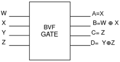
3.3.7 BVF gate
The input is represented as In={W, X, Y, Z} and the output is represented as Out={W, W$\oplus$X, Y, Y$\oplus$Z}. BVF is a double XOR gate. The BVF gate serves the purpose of extracting essential inputs to fulfill the fan-out requirements. Its block diagram is shown in Figure 24 [73].
Figure 24. BVF gate
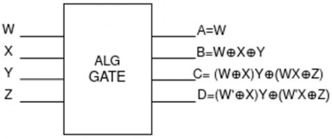
3.3.8 ALG gate
The input is represented as In={W,X,Y,Z} and the output is represented as Out={W, W$\oplus$X$\oplus$Y, (W$\oplus$X)Y$\oplus$(WX$\oplus$Z), (W’$\oplus$X)Y$\oplus$(W’X$\oplus$Z)}. The ALG gate can perform multiple operations like full adder, full subtractor, XOR, NAND, and NOR. Its block diagram is shown in Figure 25 [71].
Figure 25. ALG gate
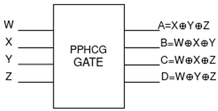
3.3.9 PPHCG gate
Parity Preserving Hamming Code Generator (PPHCG) gate preseves parity. The input is represented as In={W, X, Y, Z} and the output is represented as Out={X$\oplus$Y$\oplus$Z, W$\oplus$X$\oplus$Y, W$\oplus$X$\oplus$Z, W$\oplus$Y$\oplus$Z}. The quantum cost is 6. A PPHCG is used to ensure fault tolerance in Hamming error coding and detection circuits by preserving the input data's parity, enhancing the accuracy and reliability of error detection and correction. Its block diagram is shown in Figure 26 [63].
Figure 26. PPHCG gate
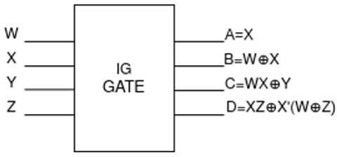
3.3.10 IG gate
The input is represented as In={W, X, Y, Z} and the output is represented as Out={X, W$\oplus$X, WX$\oplus$Y, XZ$\oplus$X’(W$\oplus$Z)} IG gate can be used to perform to perform logical operations like inverter, EX-OR, AND, EX-NOR and OR. It is a one- through gate which means one of the input variables is also the output. Its block diagram is shown in Figure 27 [74].
Figure 27. IG gate
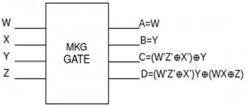
3.3.11 MKG gate
The input is represented as In={W, X, Y, Z} and the output is represented as Out={W, Y, (W’Z’$\oplus$X’)$\oplus$Y, (W’Z’$\oplus$X’)Y$\oplus$(WX$\oplus$Z)}. MKG gate is used to realize logical functions like NAND, NOT, NOR, EX-OR, AND, EX-NOR and OR. The MKG gate is categorized as a two-through gate, indicating that it has the distinct property of utilizing two of its input variables as outputs as well. Its block diagram is shown in Figure 28 [74].
Figure 28. MKG gate
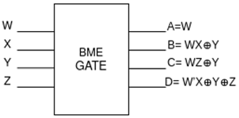
Figure 29. BME gate
3.3.12 BME gate
The input is represented as In={W, X, Y, Z} and the output is represented as Out={W, WX$\oplus$Y, WZ$\oplus$Y, W’X$\oplus$Y$\oplus$Z}. The quantum cost is 5. Its block diagram is shown in Figure 29 [68].
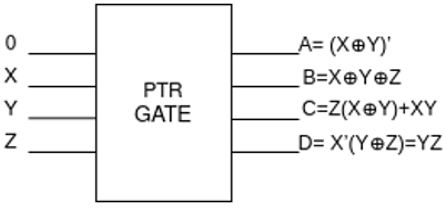
3.3.13 PTR gate
The input is represented as In={W, X, Y, Z} and the output is represented as Out={(X$\oplus$Y)’, X$\oplus$Y$\oplus$Z, Z(X$\oplus$Y)+XY, X’(Y$\oplus$Z)=YZ}. Its block diagram is shown in Figure 30 [75].
Figure 30. PTR gate
3.3.14 PAO gate
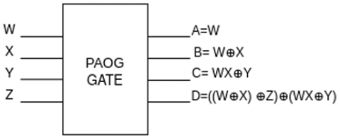
The Peres And-Or Gate (PAOG) represents an extension of the Peres gate, specifically designed for ALU (Arithmetic Logic Unit) implementation. The input is expressed as In={V,W,X,Y,Z} and the output is expressed as Out={W, W$\oplus$X, WX$\oplus$Y, ((W$\oplus$X)$\oplus$Z)$\oplus$(WX$\oplus$Y)}. The PAOG can be configured with two select inputs, allowing it to execute four unique logical operations on its two output signals. These operations encompass OR, NOR, AND, and NAND. This versatile gate has a quantum cost of 6, and its block diagram is visually represented in Figure 31 [65].
Figure 31. PAOG gate
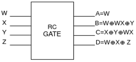
3.3.15 RC gate
The input vector of reversible comparator gate is In={W, X, Y, Z} and the output is represented as Out={W, W$\oplus$WX$\oplus$Y, X$\oplus$Y$\oplus$WX, W$\oplus$X$\oplus$Z}.The quantum cost is 5. Y and Z are the control lines when =0 and Z=1, it will compare W and X. Its block diagram is shown in Figure 32 [65].
Figure 32. RC gate
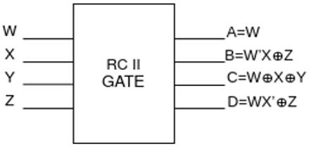
3.3.16 RC-II gate
RC-II gate is a reversible sign bit comparator. The input vector of Reversible comparator gate is In={W, X, Y, Z} and the output is represented as Out={W, W’X$\oplus$Z, W$\oplus$X$\oplus$Y, WX’$\oplus$Z}. RC-II gate is used to compare two unsigned bits. Its block diagram is shown in Figure 33 [66].
Figure 33. RC-II gate
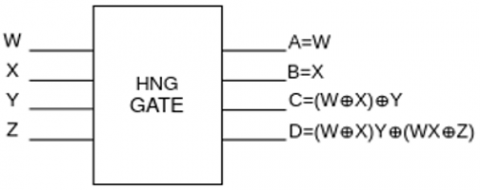
3.3.17 HNG gate
The input is represented as In={W, X, Y, Z} and the output is represented as Out={W, X, W$\oplus$X$\oplus$Y, (W$\oplus$X)Y$\oplus$(WX$\oplus$Z)}. The quantum cost of the HNG is 6. When Z=0, the circuit works as full adder. Its block diagram is shown in Figure 34 [65].
Figure 34. HNG gate
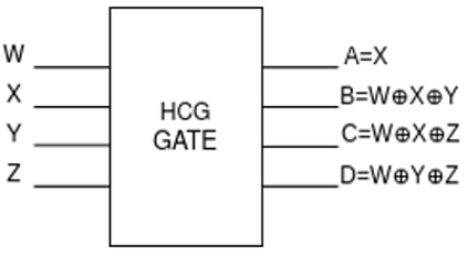
3.3.18 HCG gate
As outlined by James et al. [76], the Hamming Code Generating gate operates as a pass-through gate, wherein one of the input variables is simply mirrored as the output. Its block diagram is shown in Figure 35. The input is represented as In={W, X, Y, Z} and the output is represented as Out={X, W$\oplus$X$\oplus$Y, W$\oplus$X$\oplus$Z, W$\oplus$Y$\oplus$Z}. HCG is used to implement Hamming error coding and detection circuits [75].
Figure 35. HCG gate
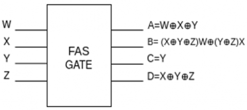
3.3.19 FAS gate
The Full Adder Subtraction (FAS) gate is capable of executing both full addition and full subtraction operations. The input is represented as In={W, X, Y, Z} and the output is represented as Out={W$\oplus$X$\oplus$Y, (X$\oplus$Y$\oplus$Z)W$\oplus$(Y$\oplus$Z)X, Y, X$\oplus$Y$\oplus$Z}. Its quantum cost is 8. Its block diagram is shown in Figure 36 [75].
Figure 36. FAS gate
3.4 5×5 reversible logic gates
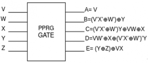
3.4.1 PPRG gate
Parity preserving reversible gate is the one through which means one of its inputs is also an output. It is a universal gate. The input is characterised as In={V, W, X, Y, Z} and the output is characterised as Out={V, (V’X’$\oplus$W’)$\oplus$Y, (V’X’$\oplus$W’)Y$\oplus$VW$\oplus$X, VW’$\oplus$X’$\oplus$(V’X’$\oplus$W’)’Y, (Y$\oplus$Z)$\oplus$VX}. P2RG gates can be singly used to build a full adder and full subtractor. Its block diagram is shown in Figure 37 [77].
Figure 37. PPRG gate
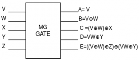
3.4.2 MG gate
Morrison gate is programmable reversible logic gate. The input is represented as In={V, W, X, Y, Z} and the output is represented as Out={V, V$\oplus$W, (V$\oplus$W)$\oplus$X,VW$\oplus$Y, ((V$\oplus$W)$\oplus$Z)$\oplus$(VW$\oplus$Y)}. The quantum cost of the MG is 7. Its block diagram is shown in Figure 38 [65].
Figure 38. MG gate
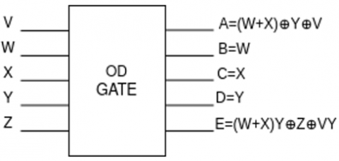
3.4.3 OD gate
The input is enumerated as In={V, W, X, Y, Z}, while the output is enumerated by Out={(W+X)$\oplus$Y$\oplus$V, W, X, Y, (W+X)Y$\oplus$Z$\oplus$VY}. Overflow Detection gate has a quantum cost of 10. OD gate is used for overflow detection. Its block diagram is shown in Figure 39 [75].
Figure 39. OD gate
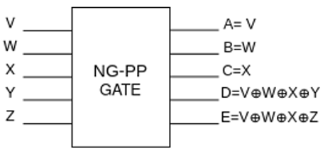
3.4.4 NG-PP
The input is characterised as In={V, W, X, Y, Z} and the output is characterised as Out={V, W, X, V$\oplus$W$\oplus$X$\oplus$Y, V$\oplus$W$\oplus$X$\oplus$Z}. The NG-PP gate incurs a quantum cost of 5, as reported by Misra et al. [78]. It is used as a parity generator and parity checker circuit [79]. Its block diagram is shown in Figure 40.
Figure 40. NG-PP gate
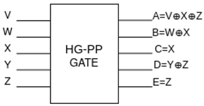
3.4.5 HG-PP gate
The input is described as In={V, W, X, Y, Z} and the output is described as Out={V$\oplus$X$\oplus$Z, W$\oplus$X, X, Y$\oplus$Z, Z}. The quantum cost of the HG-PP gate is 4. The number of 1’s in input and output are the same. HG-PP gate is used to design the hamming code [78, 80]. Its block diagram is shown in Figure 41 [75].
Figure 41. HG-PP gate
3.5 6×6 reversible logic gates
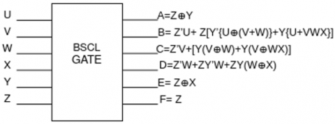
3.5.1 BSCL gate
As per Rashmi et al. [81], the Binary Coded Decimal Subtraction Correction (BSCL) gate has a dual role. It can either compute correction logic for BCD subtraction or, based on the control signal, transmit the data directly to the output.The input is represented as In={U, V, W, X, Y, Z} and the output represented as Out={Z$\oplus$Y, Z’U+Z[Y’{U$\oplus$(V+W)}+Y{U+VWX}], Z’V+[Y(V$\oplus$W)+Y(V$\oplus$WX)], Z’W+ZY’W+ZY(W$\oplus$X), Z$\oplus$X, Z}. In this context, the control signal Z dictates the output behavior: when Z equals 0; U, V, W, X, and Y are directly transmitted to the output. However, if Z equals 1 and Y is 0, the output reflects the nine's complement of the input binary number represented by U, V, W, and X. Alternatively, if Y equals 1, the output results from adding the binary number 0001 to UVWX, providing a valid corrected subtraction outcome. Its block diagram is shown in Figure 42 [75].
Figure 42. BSCL gate
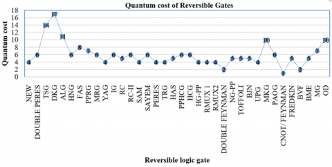
The application of reversible gates along with their quantum cost are tabulated in Table 1. The applications of some of the noteworthy reversible gates are mentioned below as well as Figure 43.
CNOT gate: CNOT gates are fundamental in creating entanglement, implementing quantum algorithms, and performing quantum error correction. CNOT gates are employed in quantum key distribution protocols. They contribute to secure communication by creating entangled states for secure key exchange between parties. In quantum teleportation protocols, CNOT gates are used to transfer the state of one quantum system to another, a process critical in quantum communication and quantum networking. Beyond Shor's and Grover's algorithms, CNOT gates are integral in various quantum algorithms, including quantum simulations, optimization problems, and quantum machine learning. CNOT gates are used in reversible logic synthesis, random number generation circuits, designing reversible circuits, and creating reversible arithmetic and data processing circuits [76, 82].
Toffoli gate (CCNOT gate): Toffoli gates play a key role in the design of quantum circuits for various applications. They are used in creating quantum adders, multicontrolled gates, and quantum carry-lookahead circuits. Toffoli gates, along with other gates, are vital in creating quantum superposition states. Superposition is a fundamental quantum property used in many quantum algorithms and quantum data representations.Toffoli gates are utilized in reversible computing to design complex reversible circuits, reversible logic synthesis, and reversible arithmetic circuits. They are also used in quantum algorithms, quantum error correction, and implementing various logic gates in quantum circuits [83, 84].
Fredkin gate (C-SWAP gate): Fredkin gates find applications in quantum permutation networks. These networks rearrange the order of quantum states, which is essential in quantum sorting algorithms and quantum data permutation tasks. The gates enable conditional swapping or routing of data in reversible data routing circuits and permutation networks. In quantum multiplexing, Fredkin gates are employed to combine and separate quantum states, a valuable process in quantum communication and networking. Fredkin gates find applications in reversible logic design, reversible arithmetic circuits, and reversible multiplexers [85-89].
Peres gate (Peres-Horodecki gate): Peres gates are used in quantum data compression techniques, facilitating the efficient storage and transmission of quantum information. Peres gates are used to detect and analyze entanglement in quantum systems. They play a role in entanglement verification protocols and quantum information processing [90-93]. In quantum key distribution, they are employed to generate secure encryption keys, which are essential for quantum secure communication. The gates contribute to quantum channel estimation, an important process in quantum communication and information transmission.
Feynman gate (Hadamard gate): Feynman gates, or Hadamard gates, create superposition and are employed in a wide range of quantum algorithms, including quantum search algorithms like Grover's algorithm [94-97].
Swap gate: Swap gates are used in quantum algorithms for reordering and swapping quantum states, such as in quantum sorting and quantum data permutation [98-100].
The research group at University of Florida designed four chips based on reversible computing. Frank published in reference [101] that cost-efficiency of irreversible computing may have hit a theromodynamic wall, whereas for reversible computing it can continue to improve [102]. These are just a few examples of the applications of different reversible gates. Each gate has its own unique functionality and can be utilized in various contexts, depending on the specific requirements of the computation or algorithm.
Table 1. Reversible logic gates summary
|
Sr. No. |
Gate Name |
Quantum Cost |
Application |
|
1 |
cnot/ feynman gate |
1 |
Duplication of output, inverter |
|
2 |
Toffoli gate |
5 |
Universal logic gate |
|
3 |
Fredkin gate |
5 |
Swap operation |
|
4 |
Peres gate |
4 |
Subtractor |
|
5 |
Double feynman gate |
2 |
Parity preserving |
|
6 |
BJN gate |
5 |
Universal logic gate |
|
7 |
RMUX1 gate |
4 |
Multiplexer |
|
8 |
TRG gate |
4 |
Subtractor |
|
9 |
NEW gate |
4 |
Adders |
|
10 |
SAM gate |
4 |
Flip-flop implementation |
|
11 |
NFT gate |
4 |
Parity preserving |
|
13 |
RC-1gate |
5 |
Comparator |
|
14 |
UPG gate |
4 |
Universal logic gate |
|
15 |
YAG gate |
4 |
AND, OR, XNOR and EXOR implementation |
|
16 |
RMUX2 gate |
4 |
Multiplexer |
|
17 |
HAS gate |
5 |
Subtractor |
|
18 |
Double peres gate |
6 |
Adders |
|
19 |
MRG gate |
6 |
AND, OR, XNOR and EXOR implementation |
|
20 |
SAYEM gate |
6 |
Flip-flop implementation |
|
21 |
tsg gate |
14 |
Adders |
|
22 |
DKG gate |
17 |
Adders |
|
23 |
SCL gate |
Not defined |
Six correction to get actual BCD sum |
|
24 |
BVF gate |
2 |
Extracting necessary outputs to meet fan-out requirements |
|
25 |
alg gate |
11 |
Adders |
|
26 |
PPHCG gate |
6 |
Hamming error coding and detection |
|
27 |
IG gate |
6 |
AND, OR, XNOR and EXOR Implementation |
|
28 |
MKG gate |
13 |
Universal logic gate |
|
29 |
bme gate |
5 |
Multiplier implementation |
|
30 |
PTR gate |
Not defined |
Adders |
|
31 |
PAOG gate |
6 |
Universal logic gate |
|
32 |
rc gate |
5 |
Comparator |
|
33 |
rc-ii gate |
5 |
Comparator |
|
34 |
hng gate |
6 |
Adders |
|
35 |
HCG gate |
6 |
Hamming error coding and detection |
|
36 |
fas gate |
8 |
Adders |
|
37 |
PPRG gate |
7 |
Adders |
|
38 |
MG gate |
7 |
ALU implementation |
|
39 |
od gate |
10 |
Overflow detection |
|
40 |
ng-pp gate |
5 |
Parity preserving |
|
41 |
HG-PP gate |
4 |
Hamming error coding and detection |
|
42 |
BSCL gate |
Not defined |
Subtraction correction |
Figure 43. Comparison of quantum cost of reversible logic gates
This comprehensive review paper serves as a meticulous exploration of reversible logic gates, taking into consideration over 50 distinct gate types, with prominent examples like the CNOT, Toffoli, and Fredkin gates. The paper's primary focus is to underscore the significant advantages associated with reversible logic, which encompasses a substantial reduction in power consumption, the pivotal aspect of information reversibility, and the notable decrease in heat generation during computation.
The applications of reversible logic gates are profoundly diverse and span a spectrum of domains. In quantum computing, these gates hold a fundamental role in the implementation of quantum algorithms and in preserving quantum coherence during operations. In the arena of low-power circuit design, where energy efficiency is a critical consideration, reversible gates have shown significant promise. They have been effectively harnessed in reversible arithmetic circuits, memory system design, and the development of error correction techniques, leading to reduced power consumption and an overall enhancement in circuit performance.
Furthermore, the exploration of reversible gates extends its reach into the field of nanotechnology. It opens avenues for the potential advancement of molecular computing, which could lead to substantial progress in miniaturized computing systems, marking a significant development in the realm of information technology.
Looking into the future, the field of reversible logic gates presents a host of opportunities for further research and innovation. These opportunities are closely tied to the field's ongoing challenges, including the design and optimization of larger reversible circuits, the development of efficient synthesis methodologies, and the exploration of new architectures and technologies that can effectively tackle the practical hurdles associated with implementation. Research in these directions promises to significantly advance the field's boundaries.
The implications arising from this review are of practical importance. Reversible logic gates are positioned to contribute substantially to energy-efficient low-power circuit design, thereby extending the life of battery-powered electronic devices and promoting sustainable energy practices. Additionally, they have the potential to strengthen the security and performance of quantum computing, which is of paramount significance in the age of data security and quantum technological advancements. Beyond these applications, reversible gates have the capacity to revolutionize the field of nanotechnology, presenting avenues for molecular computing that could lead to the development of more compact and efficient computing systems.
It is imperative to acknowledge the inherent limitations of this study. While it provides a comprehensive overview of the field, it does not delve into specific technical details. Moreover, the nature of quantum computing and its related fields is highly dynamic and continuously evolving, which means that the observations and analyses contained in this review are reflective of a specific point in time.
In summary, this review functions as a meticulously constructed map of the intricate world of reversible logic gates, highlighting their remarkable advantages and multifaceted applications. The paper’s discussion of future research directions underscores the promising outlook for the field and underscores the practical implications, which could redefine the domains of low-power circuit design, quantum computing, and nanotechnology.
[1] Mollick, E. (2006). Establishing moore's law. IEEE Annals of the History of Computing, 28(3): 62-75. https://doi.org/10.1109/MAHC.2006.45
[2] Shauly, E.N. (2012). CMOS leakage and power reduction in transistors and circuits: Process and layout considerations. Journal of Low Power Electronics and Applications, 2(1): 1-29. https://doi.org/10.3390/jlpea2010001
[3] Landauer, R. (1961). Irreversibility and heat generation in the computing process. IBM Journal of Research and Development, 5(3): 183-191. https://doi.org/10.1147/rd.53.0183
[4] Keyes, R.W., Landauer, R. (1970). Minimal energy dissipation in logic. IBM Journal of Research and Development, 14(2): 152-157. https://doi.org/10.1147/rd.142.0152
[5] Bennett, C.H. (1973). Logical reversibility of computation. IBM Journal of Research and Development, 17(6): 525-532. https://doi.org/10.1147/rd.176.0525
[6] Bennett, C.H. (1982). The thermodynamics of computation-a review. International Journal of Theoretical Physics, 21(1): 905-940. https://doi.org/10.1007/BF0208415801
[7] Pan, W.D., Nalasani, M. (2005). Reversible logic. IEEE Potentials, 24(1): 38-41. https://doi.org/10.1109/MP.2005.1405801
[8] Toffoli, T. (1980). Reversible computing. In International Colloquium on Automata, Languages, and Programming, Seventh Colloquium, Noordwijkerhout, The Netherlands, pp. 632-644. https://doi.org/10.1007/3-540-10003-2_104
[9] Gautam, P. (2014). Development of tool for mapping conventional circuit to reversible logic. arXiv preprint arXiv:1407.0632. https://doi.org/10.48550/arXiv.1407.0632
[10] Radha, N., Maheswari, M. (2020). An energy-efficient multiplier using reversible gates. Journal of Physics: Conference Series, 1706(1): 012066 https://doi.org/10.1088/1742-6596/1706/1/012066
[11] Shende, V.V., Prasad, A.K., Markov, I.L., Hayes, J.P. (2003). Synthesis of reversible logic circuits. IEEE Transactions on Computer-Aided Design of Integrated Circuits and Systems, 22(6): 710-722. https://doi.org/10.1109/TCAD.2003.811448
[12] Thapliyal, H., Ranganathan, N. (2011). A new reversible design of BCD adder. In 2011 Design, Automation & Test in Europe, Grenoble, France, pp. 1-4. https://doi.org/10.1109/DATE.2011.5763308
[13] Wille, R., Chattopadhyay, A., Drechsler, R. (2016). From reversible logic to quantum circuits: Logic design for an emerging technology. In 2016 International Conference on Embedded Computer Systems: Architectures, Modeling and Simulation (SAMOS), Agios Konstantinos, Greece, pp. 268-274. https://doi.org/10.1109/SAMOS.2016.7818357
[14] Frank, M.P., Shukla, K. (2021). Quantum foundations of classical reversible computing. Entropy, 23(6): 701. https://doi.org/10.3390/e23060701
[15] Frank, M.P. (2005). Introduction to reversible computing: Motivation, progress, and challenges. In Proceedings of the 2nd Conference on Computing Frontiers, Ischia Italy, pp. 385-390. https://doi.org/10.1145/1062261.1062324
[16] Peres, A. (1985). Reversible logic and quantum computers. Physical Review A, 32(6): 3266-3276. https://doi.org/10.1103/PhysRevA.32.3266
[17] Fredkin, E., Toffoli, T. (1982). Conservative logic. International Journal of Theoretical Physics, 21(3-4): 219-253. https://doi.org/10.1007/BF01857727
[18] Barenco, A., Bennett, C.H., Cleve, R., DiVincenzo, D.P., Margolus, N., Shor, P., Sleator, T., Smolin, J.A., Weinfurter, H. (1995). Elementary gates for quantum computation. Physical Review A, 52(5): 3457-3467. https://doi.org/10.1103/PhysRevA.52.3457
[19] Perkowski, M., Khan, M.H.A. (2011). Synthesis of reversible synchronous counters. In 2011 41st IEEE International Symposium on Multiple-Valued Logic, Tuusula, Finland, pp. 242-247. https://doi.org/10.1109/ISMVL.2011.25
[20] Iwama, K., Kambayashi, Y., Yamashita, S. (2002). Transformation rules for designing CNOT-based quantum circuits. In Proceedings of the 39th annual Design Automation Conference, New Orleans Louisiana USA, pp. 419-424. https://doi.org/10.1145/513918.514026
[21] Miller, D.M., Maslov, D., Dueck, G.W. (2003). A transformation based algorithm for reversible logic synthesis. In Proceedings of the 40th annual Design Automation Conference, Anaheim CA USA, pp. 318-323. https://doi.org/10.1145/775832.775915
[22] Dueck, G.W., Maslov, D., Miller, D.M. (2003). Transformation-based synthesis of networks of Toffoli/Fredkin gates. In CCECE 2003 - Canadian Conference on Electrical and Computer Engineering. Toward a Caring and Humane Technology, Montreal, QC, Canada, pp. 211-214. https://doi.org/10.1109/CCECE.2003.1226380
[23] Maslov, D., Dueck, G.W., Miller, D.M. (2005). Synthesis of Fredkin-Toffoli reversible networks. IEEE Transactions on Very Large Scale Integration (VLSI) Systems, 13(6): 765-769. https://doi.org/10.1109/TVLSI.2005.844284
[24] Arabzadeh, M., Saeedi, M., Saheb Zamani, M. (2010). Rule-based optimization of reversible circuits. In Proceedings of the 2010 Asia and South Pacific Design Automation Conference, Taipei, Taiwan, pp. 849-854. https://doi.org/10.1109/ASPDAC.2010.5419684
[25] Yang, G., Song, X., Hung, W.N., Xie, F., Perkowski, M.A. (2006). Group theory based synthesis of binary reversible circuits. In International Conference on Theory and Applications of Models of Computation, Beijing, China, pp. 365-374. https://doi.org/10.1007/11750321_35
[26] Sasanian, Z., Saeedi, M., Sedighi, M., Zamani, M.S. (2009). A cycle-based synthesis algorithm for reversible logic. In Design Automation Conference, Yokohama, Japan, pp. 745-750. https://doi.org/10.1109/ASPDAC.2009.4796569
[27] Kerntopf, P. (2004). A new heuristic algorithm for reversible logic synthesis. In DAC04: The 41st Annual Design Automation Conference 2004, San Diego, CA USA, pp. 843-837. https://doi.org/10.1145/996566.996789
[28] Wille, R., Drechsler, R. (2009). BDD-based synthesis of reversible logic for large functions. In Proceedings of the 46th Annual Design Automation Conference, San Francisco, California, pp. 270-275. https://doi.org/10.1145/1629911.1629984
[29] Gupta, P., Agarwal, A., Jha, N.K. (2006). An algorithm for synthesis of reversible logic circuits. IEEE Transactions on Computer-Aided Design, 25(11): 2317-2330. https://doi.org/10.1109/TCAD.2006.871622
[30] Maslov, D., Dueck, G.W. (2004). Reversible cascades with minimal garbage. IEEE Transactions on Computer-Aided Design, 23(11): 1497-1509. https://doi.org/10.1109/TCAD.2004.836735
[31] Yang, G., Song, X., Hung, W.N.N., Perkowski, M.A. (2008). Bi-directional synthesis of 4-bit reversible circuits. Computer Journal, 51(2): 207-215. https://doi.org/10.1093/comjnl/bxm042
[32] Prasad, A.K., Shende, V.V., Markov, I.L., Hayes, J.P., Patel, K.N. (2006). Data structures and algorithms for simplifying reversible circuits. ACM Journal on Emerging Technologies in Computing Systems (JETC), 2(4): 277-293. https://doi.org/10.1145/1216396.1216399
[33] Donald, J., Jha, N.K. (2008). Reversible logic synthesis with Fredkin and Peres gates. Journal of Emerging Technologies in Computing Systems, 4(1): 1-19. https://doi.org/10.1145/1330521.1330523
[34] Maslov, D., Saeedi, M. (2011). Reversible circuit optimization via leaving the Boolean domain. IEEE Transactions on Computer-Aided Design of Integrated Circuits and Systems, 30(6): 806-816. https://doi.org/10.1109/TCAD.2011.2105555
[35] Saeedi, M., Zamani, M.S., Sedighi, M., Sasanian, Z. (2010). Reversible circuit synthesis using a cycle-based approach. ACM Journal on Emerging Technologies in Computing Systems (JETC), 6(4): 1-26. https://doi.org/10.1145/1877745.1877747
[36] Bruce, J.W., Thornton, M.A., Shivakumaraiah, L., Kokate, P.S., Li, X. (2002). Efficient adder circuits based on a conservative reversible logic gate. In Proceedings IEEE Computer Society Annual Symposium on VLSI. New Paradigms for VLSI Systems Design. ISVLSI 2002, Pittsburgh, PA, USA, pp. 83-88. https://doi.org/10.1109/ISVLSI.2002.1016879
[37] Tiwari, K., Khopade, A., Jadhav, P. (2011). Optimized carry look-ahead BCD adder using reversible logic. In Technology Systems and Management: First International Conference, ICTSM 2011, Mumbai, India, pp. 260-265. https://doi.org/10.1007/978-3-642-20209-4_37
[38] Khan, M.H., Perkowski, M.A. (2007). Quantum ternary parallel adder/subtractor with partially-look-ahead carry. Journal of Systems Architecture, 53(7): 453-464. https://doi.org/10.1016/j.sysarc.2007.01.007
[39] Vasudevan, D., Goudarzi, M., Popovici, E., Schellekens, M. (2009). A reversible MIPS multi-cycle control FSM design. In 2009 1st Asia Symposium on Quality Electronic Design, Kuala Lumpur, Malaysia, pp. 336-342. https://doi.org/10.1109/ASQED.2009.5206242
[40] Vedral, V., Barenco, A., Ekert, A. (1996). Quantum networks for elementary arithmetic operations. Physical Review A, 54(1): 147-153. https://doi.org/10.1103/PhysRevA.54.147
[41] Abdessaied, N., Drechsler, R., Abdessaied, N., Drechsler, R. (2016). Optimizations and complexity analysis on the quantum level. Reversible and Quantum Circuits: Optimization and Complexity Analysis, 141-174. https://doi.org/10.1007/978-3-319-31937-7_5
[42] Banerjee, A., Pathak, A. (2009). An algorithm for minimization of quantum cost. arXiv preprint arXiv:0910.2129. https://doi.org/10.48550/arXiv.0910.2129
[43] Haghparast, M., Navi, K. (2008). Design of a novel fault tolerant reversible full adder for nanotechnology based systems. World Applied Sciences Journal, 3(1): 114-118. https://doi.org/10.3844/ajassp.2008.282.288
[44] Islam, M.S., Rahman, M.M., Begum, Z., Hafiz, M.Z. (2009). Fault tolerant reversible logic synthesis: Carry look-ahead and carry-skip adders. In 2009 International Conference on Advances in Computational Tools for Engineering Applications, Beirut, Lebanon, pp. 396-401. https://doi.org/10.1109/ACTEA.2009.5227871
[45] Mitra, S.K., Chowdhury, A.R. (2012). Minimum cost fault tolerant adder circuits in reversible logic synthesis. In 2012 25th International Conference on VLSI Design, Hyderabad, India, pp. 334-339. https://doi.org/10.1109/VLSID.2012.93
[46] Parhami, B. (2006). Fault-tolerant reversible circuits. In Proceedings of the Fortieth Asilomar Conference on Signals, Systems and Computers (ACSSC), Pacific Grove, CA, USA, pp. 1726-1729. https://doi.org/10.1109/ACSSC.2006.355056
[47] Möller, M., Vuik, C. (2017). On the impact of quantum computing technology on future developments in high-performance scientific computing. Ethics and Information Technology, 19: 253-269. https://doi.org/10.1007/s10676-017-9438-0
[48] Buhrman, H., Cleve, R., Watrous, J., de Wolf, R. (2001). Quantum fingerprinting. Physical Review Letters, 87(16): 167902. https://doi.org/10.1103/PhysRevLett.87.167902
[49] Horn, R.T., Babichev, S.A., Marzlin, K.P., Lvovsky, A.I., Sanders, B.C. (2005). Single-qubit optical quantum fingerprinting. Physical Review Letters, 95(15): 150502. https://doi.org/10.1103/PhysRevLett.95.150502
[50] Gottesman, D., Chuang, I. (2001). Quantum digital signatures. arXiv preprint quant-ph/0105032. https://doi.org/10.48550/arXiv.quant-ph/0105032
[51] Shende, V.V., Bullock, S.S., Markov, I.L. (2005). Synthesis of quantum logic circuits. In Proceedings of the 2005 Asia and South Pacific Design Automation Conference, Shanghai China, pp. 272-275. https://doi.org/10.1145/1120725.1120847
[52] Abdollahi, A., Pedram, M. (2006). Analysis and synthesis of quantum circuits by using quantum decision diagrams. In Proceedings of the Design Automation & Test in Europe Conference, Munich, Germany, pp. 1-6. https://doi.org/10.1109/DATE.2006.244176
[53] Ruican, C., Udrescu, M., Prodan, L., Vladutiu, M. (2007). Automatic synthesis for quantum circuits using genetic algorithms. In Adaptive and Natural Computing Algorithms: 8th International Conference, ICANNGA 2007, Warsaw, Poland, pp. 174-183. https://doi.org/10.1007/978-3-540-71618-1_20
[54] De Vos, A. (2011). Reversible Computing: Fundamentals, Quantum Computing, and Applications. John Wiley & Sons. https://doi.org/10.1002/9783527633999
[55] Swathi, M., Rudra, B. (2021). Implementation of reversible logic gates with quantum gates. In 2021 IEEE 11th Annual Computing and Communication Workshop and Conference (CCWC), NV, USA, pp. 1557-1563. https://doi.org/10.1109/CCWC51732.2021.9376060
[56] Berman, G.P. (1998). Introduction to Quantum Computers. Singapore: World Scientific. https://doi.org/10.1142/3808
[57] Hänninen, I., Lu, H., Blair, E.P., Lent, C.S., Snider, G.L. (2014). Reversible and adiabatic computing: Energy-efficiency maximized. Field-Coupled Nanocomputing: Paradigms, Progress, and Perspectives, 341-356. https://doi.org/10.1007/978-3-662-43722-3_14
[58] Mohammadi, M., Eshghi, M. (2009). On figures of merit in reversible and quantum logic designs. Quantum Information Processing, 8: 297-318. https://doi.org/10.1007/s11128-009-0106-0
[59] Feynman, R.P., Hey, T. (2023). Quantum mechanical computers. In Feynman Lectures on Computation, pp. 169-192. https://doi.org/10.1364/ON.11.2.000011
[60] Rajput, A.K., Chouhan, S., Pattanaik, M. (2019). Low power boolean logic circuits using reversible logic gates. In 2019 International Conference on Advances in Computing, Communication and Control (ICAC3), Mumbai, India, pp. 1-6. https://doi.org/10.1109/ICAC347590.2019.9036799
[61] Fedorov, A., Steffen, L., Baur, M., da Silva, M.P., Wallraff, A. (2012). Implementation of a Toffoli gate with superconducting circuits. Nature, 481: 170-172. https://doi.org/10.1038/nature10713
[62] Kolay, S.C., Chattopadhyay, S., Bandyopadhyay, M. (2020). Design and development of SS reversible logic gate and it’s application as adder & subtractor. In 2020 International Conference on Inventive Computation Technologies (ICICT), Coimbatore, India, pp. 977-981. https://doi.org/10.1109/ICICT48043.2020.9112514
[63] Gaur, H.M., Singh, A.K., Mohan, A., Pradhan, D.K. (2019). Computational analysis and comparison of reversible gates for design and test of logic circuits. International Journal of Electronics, 106(11): 1679-1693. https://doi.org/10.1080/00207217.2019.1608587
[64] Islam, M.S., Begum, Z. (2010). Reversible logic synthesis of fault tolerant carry skip BCD adder. Journal of Bangladesh Academy of Sciences, 32(2): 234-250. https://doi.org/10.3329/jbas.v32i2.2431
[65] Singh, S., Choudhary, A., Jain, M.K. (2019). A brief overview of reversible logic gate and reversible circuits. International Journal of Electronics Engineering, 11(2): 86-104.
[66] Morrison, M. (2012). Design of a reversible alu based on novel reversible logic structures. University of South Florida. In IEEE Computer Society Annual Symposium on VLSI, pp. 126-131. https://doi.org/10.1109/ISVLSI.2011.30
[67] Sharmin, F., Mitra, R.K., Hasan, R., Rahman, A. (2013). Low cost reversible signed comparator. International Journal of VLSI design & Communication Systems, 4(5): 19. https://doi.org/10.5121/vlsic.2013.4502
[68] Misra, N.K., Wairya, S., Singh, V. K. (2015). Frame of reversible BCD adder and carry skip BCD adder and optimization using new reversible logic gates for quantum-dot cellular automata. Australian Journal of Basic and Applied Sciences, 9(31): 286-298.
[69] Samrin, S.S., Patil, R., Itagi, S., Chetti, S.C., Tasneem, A. (2022). Design of logic gates using reversible gates with reduced quantum cost. Global Transitions Proceedings, 3(1): 136-141. https://doi.org/10.1016/j.gltp.2022.04.011
[70] Bhagyalakshmi, H.R., Venkatesha, M.K. (2011). Optimized design of BCD adder and carry skip BCD adder using reversible logic gates. International Journal on Computer Science and Engineering, 3(4): 1439-1449.
[71] Arun, M., Saravanan, S. (2013). Reversible arithmetic logic gate (ALG) for quantum computation. International Journal of Intelligent Engineering and Systems, 6(3): 1-9. https://doi.org/10.22266/ijies2013.9030.01.
[72] Krishnaveni, D., Priya, G.M. (2011). A novel design of reversible serial and parallel adder/subtractor. International Journal of Engineering Science and Technology, 3(3): 2280-2288.
[73] Krishnaveni, D., Priya, M.G., Baskaran, K. (2012). Design of an efficient reversible 8x8 Wallace tree multiplier. World Applied Sciences Journal, 20(8): 1159-1165. https://doi.org/10.5829/idosi.wasj.2012.20.08.711
[74] Haghparast, M., Navi, K. (2007). A novel reversible full adder circuit for nanotechnology based systems. Journal of Applied Sciences, 7(24): 3995-4000. https://doi.org/10.3923/jas.2007.3995.4000
[75] Prakash, D.N.R., Pannu, N. (2013). Generalised approaches for ALU design using reversible gates. International Journal of Computer Science and Information Technologies, 6(6): 5292-5294
[76] James, R.K., Shahana, T.K., Jacob, K.P., Sasi, S. (2007). Fault tolerant error coding and detection using reversible gates. In TENCON 2007 IEEE Region 10 Conference, Taipei, Taiwan, pp. 1-4, https://doi.org/10.1109/TENCON.2007.4428776
[77] Saini, S., Khandelwal, R. (2015). Parity preserving adder/subtractor using a novel reversible gate. In IEEE Fifth International Conference on Communication Systems and Network Technologies, Gwalior, India, pp. 885-888. https://doi.org/10.1109/CSNT.2015.14
[78] Misra, N.K., Wairya, S., Singh, V.K. (2015). Frame of reversible BCD adder and carry skip BCD adder and optimization using new reversible logic gates for quantum-dot cellular automata. Australian Journal of Basic and Applied Sciences, 9(31): 286-298
[79] Misra, N.K., Sen, B., Wairya, S. (2017). Novel conservative reversible error control circuits based on molecular QCA. International Journal of Computer Applications in Technology. 56(1): 1-17. https://doi.org/10.1504/IJCAT.2017.086558
[80] Galadima, B.Y., Galadanci, G.S.M., Tijjani, A., Ibrahim, M. (2020). A review on reversible logic gates. Bayero Journal of Pure and Applied Sciences, 12(1): 242-250. https://doi.org/10.4314/bajopas.v12i1.38S
[81] Rashmi, S. B., Praveen, B., Tilak B.G. (2011). Design of optimized reversible BCD adder/subtractor. International Journal of Engineering and Technology. 3(3): 230-234. https://doi.org/10.7763/IJET.2011.V3.229
[82] Orts, F., Filatovas, E., Garzón, E.M., Ortega, G. (2023). A quantum circuit to generate random numbers within a specific interval. EPJ Quantum Technology, 10(1): 17. https://doi.org/10.1140/epjqt/s40507-023-00174-1
[83] Cheng, C.S., Singh, A.K., Gopal, L. (2015). Efficient three variables reversible logic synthesis using mixed-polarity Toffoli gate. Procedia Computer Science, 70: 362-368. https://doi.org/10.1016/j.procs.2015.10.035
[84] Golubitsky, O., Maslov, D. (2011). A study of optimal 4-bit reversible Toffoli circuits and their synthesis. IEEE Transactions on Computers, 61(9): 1341-1353. https://doi.org/10.1109/TC.2011.144
[85] Naz, S.F., Ahmed, S., Sharma, S., Ahmad, F., Ajitha, D. (2021). Fredkin gate based energy efficient reversible D flip flop design in quantum dot cellular automata. Materials Today: Proceedings, 46: 5248-5255. https://doi.org/10.1016/j.matpr.2020.08.634
[86] Dovhaniuk, O., Deibuk, V. (2021). Synthesis and implementation of reconfigurable reversible generalized Fredkin gate. In IEEE 12th International Conference on Electronics and Information Technologies, Lviv, Ukraine, pp. 165-169. https://doi.org/10.1109/ELIT53502.2021.9501129
[87] Nikitin, M.S., Nikitina, K.A., Tyurin, S.F. (2022). Design and investigation of a bidirectional Fredkin gate. In 2022 Conference of Russian Young Researchers in Electrical and Electronic Engineering, Saint Petersburg, Russian Federation, pp. 812-816. https://doi.org/10.1109/ElConRus54750.2022.9755514
[88] Joy, K., Mathew, B.K. (2014). Implementation of a FIR filter model using reversible Fredkin gate. In International Conference on Control, Instrumentation, Communication and Computational Technologies, pp. Kanyakumari, India, pp. 690-694. https://doi.org/10.1109/ICCICCT.2014.6993048
[89] Nikhil, G., Sharanya, B., Reddy, P.B., Vidyadhar, R.P. (2021). Reversible 2:4 decoder using universal Fredkin gate. In 6th International Conference on Communication and Electronics Systems, Coimbatre, India, pp. 173-176. https://doi.org/10.1109/ICCES51350.2021.9489226
[90] Thabah, S.D., Saha, P. (2020). New design approaches of reversible BCD encoder using Peres and Feynman gates. ICT Express, 6(1): 38-42. https://doi.org/10.1016/j.icte.2019.07.001
[91] Thomsen, M.K., Glück, R. (2008). Optimized reversible binary-coded decimal adders. Journal of Systems Architecture, 54(7): 697-706. https://doi.org/10.1016/j.sysarc.2007.12.006
[92] PourAliAkbar, E., Mosleh, M. (2019). An efficient design for reversible Wallace unsigned multiplier. Theoretical Computer Science, 773: 43-52. https://doi.org/10.1016/j.tcs.2018.06.007
[93] Barati, R. (2022). High speed low power multipliers based on reversible logic methods. e-Prime-Advances in Electrical Engineering, Electronics and Energy, 2: 100033. https://doi.org/10.1016/j.prime.2022.100033
[94] AnanthaLakshmi, A.V., Sudha, G.F. (2017). A novel power-efficient 0.64-GFlops fused 32-bit reversible floating-point arithmetic unit architecture for digital signal processing applications. Microprocessors and Microsystems, 51: 366-385. https://doi.org/10.1016/j.micpro.2017.01.002
[95] Majumder, A., Singh, P.L., Chowdhury, B., Mondal, A. J., Anand, V. (2015). Efficient design and analysis of N-bit reversible shift registers. Procedia Computer Science, 57: 199-208. https://doi.org/10.1016/j.procs.2015.07.431
[96] Shukla, V., Singh, O.P., Mishra, G.R., Tiwari, R.K. (2018). Reversible realization of N-bit arithmetic circuit for low power loss ALU applications. Procedia Computer Science, 125: 847-854. https://doi.org/10.1016/j.procs.2017.12.108
[97] Mirizadeh, S.M.A., Asghari, P. (2022). Fault-tolerant quantum reversible full adder/subtractor: Design and implementation. Optik, 253: 168543. https://doi.org/10.1016/j.ijleo.2021.168543
[98] Kole, A., Datta, K., Sengupta, I. (2016). A heuristic for linear nearest neighbor realization of quantum circuits by swap gate insertion using N-gate lookahead. IEEE Journal on Emerging and Selected Topics in Circuits and Systems, 6(1): 62-72. https://doi.org/10.1109/JETCAS.2016.2528720
[99] Copsey, D., Oskin, M., Impens, F., Metodiev, T., Cross, A., Chong, F.T., Chuang, I.L., Kubiatowicz, J. (2003). Toward a scalable, silicon-based quantum computing architecture. IEEE Journal of Selected Topics in Quantum Electronics, 9(6): 1552-1569. https://doi.org/10.1109/JSTQE.2003.820922
[100] Lin, S.F., Sussman, S., Duckering, C., Mundada, P.S., Baker, J.M., Kumar, R.S., Houck, A.A., Chong, F.T. (2022). Let each quantum bit choose its basis gates. In 2022 55th IEEE/ACM International Symposium on Microarchitecture (MICRO), Chicago, IL, USA, pp. 1042-1058. https://doi.org/10.1109/MICRO56248.2022.00075
[101] https://www.cise.ufl.edu/research/revcomp/, accessed on 20 March 2023.
[102] Frank, M.P. (2006). Nanocomputer Systems Engineering. Boca Raton: CRC Press.