Leena Ali | Muhammad Ilyas![]() | Taha A. Elwi*
| Taha A. Elwi*![]()
© 2023 IIETA. This article is published by IIETA and is licensed under the CC BY 4.0 license (http://creativecommons.org/licenses/by/4.0/).
OPEN ACCESS
A novel compact antenna array design, tailored for 5G applications, is introduced in this paper. The proposed antenna operates in the sub-6GHz frequency range, ensuring optimal wave propagation characteristics in local areas. To achieve this, a Hilbert fractal patch-based design is employed. The antenna is developed as a two-element array, catering to Multi-Input Multi-Output (MIMO) communication systems. The overall size of the antenna array is reduced by minimizing the spacing between the antenna elements, which is achieved through the integration of Metamaterial (MTM) Minkowski inclusions as defects on the back panel. The antenna exhibits a gain greater than 4.7dBi within the targeted frequency band, with a maximum coupling of -20dB. Two primary frequency bands, centered around 3.5 GHz and 5.5 GHz, are demonstrated by the antenna array. The proposed design is fabricated and subsequently subjected to experimental testing. The measured results exhibit excellent agreement with their corresponding simulation outcomes, confirming the effectiveness of the proposed antenna design.
MIMO, MTM, 5G, Hilbert, Minkowski, fractal
In recent years, the rapid development of mobile communication networks has necessitated the need to satisfy increasing demands for data rates within the range of gigabits-per-second [1, 2]. As a result, the urgency to develop modern antenna designs that cater to contemporary wireless communication systems has become paramount [3]. However, designing antennas with wide bandwidth and enhanced gain is challenged by the constraint of antenna size limitations [4]. To address these challenges, researchers have employed various techniques, such as the composite right-left-hand microstrip antenna with an enhanced gain bandwidth product for RF energy harvesting at 2.45 GHz and 5.8 GHz, as presented in the studies [5, 6]. Additionally, low-profile fractal antenna structures based on Metamaterial (MTM) arrays have been developed for modern Wi-Fi systems [7]. A circularly polarized fractal antenna structure based on the Koch-snowflake 1st iteration was proposed for 5G handset systems, with the antenna ground plane featuring MTM unit cell defects [8, 9].
MTMs have significantly contributed to the advancement of antenna systems due to their unique properties, characterized by exceptional electromagnetic constitutive parameters [10]. In the study [11], certain MTM inclusions were incorporated into an antenna patch to control the beam steering capacity using two semiconductor switches. Another study [12] utilized an MTM layer on top of an antenna patch to enhance antenna gain at Wi-Fi bands. The integration of MTM structures into the antenna ground plane was explored in the study [13] to minimize back lobe effects at 3.4 GHz. A different approach was proposed in the study [14], employing MTM to ensure antenna surface wave propagation toward the end-fire direction for gain-bandwidth enhancements. Lastly, an MTM antenna design was presented in study [15], resulting in a gain enhancement at 4.6 GHz for 5G communication networks.
Nevertheless, certain limitations persist in existing designs. For instance, the microstrip antenna array for 5G networks at 28 GHz bands, based on 4×4 elements, as presented in study [16], suffered from limited propagation, which was not addressed in their work. Another design, proposed in study [17], utilized a triple-band with dual polarization printed circuit antenna array for MIMO systems in the sub-6 GHz for 5G applications. An antenna developed for 5G applications, using a 3D profile of four printed antenna elements separated with MTM defects, provided high gain bandwidth. However, the complex structure was impractical for low-profile devices [18]. A reconfigurable antenna element with optical switches was proposed in study [19], but the array systems analysis was not considered. In study [20], a microstrip antenna based on MTM defects was proposed for the same application, but with limited gain at a single frequency band.
In this work, a novel antenna array design based on an MTM array is proposed, aiming to achieve a miniaturized antenna structure for 5G communication networks. The proposed MTM arrays are mounted parallel to a conductive trace, ensuring in-phase reflection characteristics and high-impedance response while mitigating the effects of surface wave retardation from the antenna edges. This technique demonstrates gain-bandwidth enhancements over conventional printed antenna structures [16], as will be proven later. In Section II, the antenna's geometrical details are presented. The antenna design methodology is discussed in Section III. The obtained results are analyzed in Section IV. The antenna fabrication and testing are provided in Section V. Finally, the paper is concluded in Section VI.
Figure 1. Antenna design based on the proposed MTM array
The proposed antenna in this work, see Figure 1, is consistent with 4 main parts: The feeding structure based on a CPW, the T-Stub structure, the Hilbert fractal patch, and the MTM layer. These structures are printed together on the same substrate based on tectonics FR-4 epoxy polymer of εr=4.3 with tanδ=0.000078. The antenna is configured as an array of two elements for MIMO applications with a maximum size of 50mm×37mm. The authors, conducted in their design the use of the proposed CPW to feed their antenna because, in such a technique, the transmission line and the ground plane are mounted on the same side of the substrate. Therefore, in such a structure, the effects of the generated surface waves may realize minimum effects on the patch operation. Using such a structure operate at a wide frequency bandwidth with minimum effects of capacitive and inductive losses due to the location of the ground plane on the same side of the transmission line [11]. Particularly for this work, the authors picked such a technique to ensure keeping the other side of the substrate is free to lunch the proposed MTM structure. The other part of the proposed antenna element is the use of a T-stub structure to couple the electromagnetic energy capacitively to the patch geometry [13]. In such a process, intenerate losses could be realized due to the effects of conservation losses in the resulting capacitor [11]. Therefore, it is very important to consider that in the patch geometry to be constructed as an inductor behavior to eliminate the effects of the capacitive load. Moreover, the effects of the capacitive load are very important to enhance the antenna bandwidth [4] for the proposed applications. Next, the patch geometry is constructed as a Hilbert shape of the 3rd order to increase the number of frequency resonances within the frequency band of interest [6]. Consequently, the use of the proposed MTM structure when it is shaped as a Minkowski fractal of the 4th order satisfies the number of the generated bands. Such MTM is designed to eliminate the effects of coupling at the frequency band of interest [8]. For more geometrical details, the authors presented the antenna design in Figure 1.
The proposed MTM design, see Figure 1, is discussed in this section. The analysis is conducted based on a full wave simulation and circuit transmutation line. This design is structured from 6unit cells to realize an excellent frequency cut-off sharpness [5]. Each unit cell the structure third Minkowski to provide MTM left-hand properties at the frequency band on interest [6]. Therefore, the design circuit model is described in Figure 2(a). In this circuit model, it is assumed that Cl and Lc are the representation of the left-hand branch; in which, the phase of wave propagation is out of energy flow [9]. This is observed in the band gap of phase variation with frequency in Figure 2(b). Furthermore, from the evaluated S-parameters, S11 and S12, in Figures 2(c) and 2(d), respectively, cut-off bands are found in the spectrum at the desired frequency. Such observation mainly is due to stored energy in the capacitive inductive part [10]. The effects of coupling, inductive and capacitive, are given by LR and CR; between the proposed unit cell parts [2], described as the right-hand branch finally for validation numerical simulation based on CST MWS is invoked to evaluate the proposed unit cell performance. It is found an excellent agreement between the obtained results from both CST MWS and the circuit model. The lumped element of the proposed model values is listed in Table 1.
Table 1. Circuit model lumped elements
|
Lumped element |
Value |
|
LT |
0.1 nH |
|
RT |
50 Ω |
|
CT |
40 pF |
|
L1 |
1.1 nH |
|
C |
35 pF |
|
R |
70Ω |
|
L |
0.2 nH |
Figure 2. MTM unit cell performance: (a) circuit model, (b) dispersion diagram, (c) S11 spectra, and (d) S12 spectra
In this section, the authors applied a parametric study to arrive at the optimal antenna array design by using a numerical technique based on CST MWS software package therefore; the design procedure is divided into two mean parts:
4.1 Single patch study
4.1.1 T- stub
The authors introduce the design of the proposed t-stub after conducting the parametric study by changing the width (w) from 3mm to 6mm with the step of 1mm. The main reason for considering that small size, in their study, is to maintain the antenna size redaction, as will see later, and ensure a high field gradient [12]. It is found from the resented result in Figure 3(a), insignificant variations in the frequency resonant due to changing the parameter w. However, the frequency band of interest at 4.3GHz. Therefore, the authors consider the width of the T-stub (w=3) as the optimum choice in which realis fundamental mode with an excellent matching and best radiation properties to give again of 1.5dBi as shown in Figure 3(b).
Figure 3. Antenna performance variation with the width of the proposed T-stub change only: (a) S11 and (b) gain spectra
4.1.2 Hilbert effects
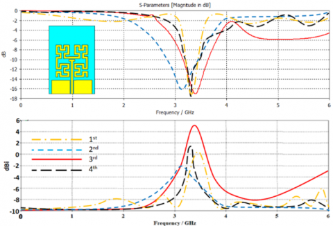
For this, the proposed patch geometry is studied numerically by changing the Hilbert order from the 1st iteration to the 4th iteration with the aim of monitoring the effects of that on the antenna S11 and gain. As seen in Figure 4(a), the number of the generated frequency resonances is increased with increasing the Hilbert iteration order up to 4 bands. However, when the 4th order is considered, the generated modes crossed the frequency band with a significant degradation in the machining impedance. Nevertheless, the effect of varying the iteration number on the antenna gain is significantly changed. It is found that the proposed antenna gain is about 5.6dBi at 3.5GHz for the case of the 3rd iteration. The proposed antenna based on the 4th iteration shows less gain, about 1.8dBi, at 3.5GHz. Therefore, the authors considered the 3rd iteration of the proposed Hilbert as the best choice for this design.
Next, it is good to consider the effects of the coupling distance (d) between the proposed t-stub and Hilbert geometry. Thus, the distance is changed for this study from 1mm to 4mm with a step of 1mm it is found from the results that are presented in Figure 5(a), an excellent enhancement is achieved in the antenna bandwidth with a significant change in the antenna gain, see Figure 5(b) this is at reputed to the effect of coupling lose that realizes a capacitive storing effect indeed, the distance (d =2mm) to maintain energy fringing a fundamental mode with storing effect which maintaining maximum gain achievement.
Figure 4. Antenna performance variation with fractal iteration change only: (a) S11 and (b) gain spectra
Figure 5. Antenna performance variation with fractal iteration change only: (a) S11 and (b) gain spectra
4.1.3 CPW effects
The proposed antenna is the with CPW structure as seen in Figure 1. The authors conducted, therefore, by changing the air gap distance from 0.1mm to 0.7mm with the step of 0.3mm parameter. It is found increasing the distance GA by more than 0.1mm reduces the antenna matching significantly. This is due to the fact of increasing the capacitive coupling loss respectively to t-stub; that emendates the surface current in the air gap [9]. Therefore, keeping the distance to the minim at 0.1mm is the best choice the obtained result from this parametric study is presented in S11 spectra as depicted in Figure 6(a). No significant effects on the antenna gain are found after increasing GA parameters as shown in Figure 6(b).
Moreover, the effects of changing the ground plane length (LG) are studied by changing it parametrically from 5mm to 10 mm with the step of 2.5mm. The effects of this variation are monitored with respect to the S11 spectrum. We found that the proposed antenna matching impedance gets much better at 7.5mm in comparison to other cases in Figure 7(a). Such enhancement is attributed to the effect of the inductive coupling increase by the Hilbert geometry and the surface way diffraction from the antenna ages [3]. This is because surface wave retardation is a common side effect in CPW antenna designs [5]. Also, the proposed antenna gain is found to significantly increase the antenna gain as shown in Figure 7(b).
Figure 6. Antenna performance variation with fractal iteration change only: (a) S11 and (b) gain spectra
Figure 7. Antenna performance variation with fractal iteration change only: (a) S11 and (b) gain spectra
4.2 MIMO array study
4.2.1 Without MTM
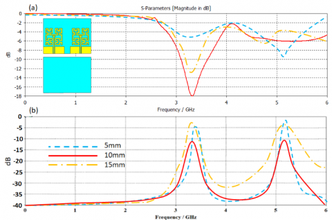
The effects of separation distance (s) between the antenna elements are changed from 5mm to 15mm with the step of 5mm with the aim to evaluate the effects of that on the S-parameters (S11 and S12). As seen in Figure 8(a), the frequency resonant is shifted significantly at the fundamental mode away from 3.5GHz as can be seen from the S11 spectra. This is due to the effects of coupling from adjacent antenna elements. Also, the antenna frequency resonance is found to be significantly affected by high degradation in matching impedance. On the other hand, the effect of coupling is found to be significantly reduced by increasing the separation parameter. This result is agreed well with the published results [6] and the effect of surface wave degradation with distance [4]. Therefore, the proposed antenna array separation distance is fixed to 10mm to ensure low coupling with minimum distance. However, the coupling effect is found to be less -10dB, see Figure 8(b) that is motivated the authors to consider MTM introduction an urgent need for that as will be seen in the next section.
Figure 8. Antenna array S-parameters variation with changing the separation distance: (a) S11 and (b) S12 spectra
4.2.2 With MTM
Now, the proposed MTM structure introduction to the antenna array performance in terms of S11 and S12 spectra. For this, the authors numerically changed the distance between the antenna elements from 5mm to 15mm with the step of 5mm. It is observed a significant enhancement in the antenna bandwidth due to the proposed MTM introduction is seen in Figure 9(a). We found that the proposed antenna array mutual coupling in terms of the S12 spectrum is dropped to -20 at the frequency band of interest when S is fixed to 5mm. Nevertheless, increasing the introduction of the proposed MTM structure reduced the antenna array mutual coupling S12 below -20 with insignificant variation in the bandwidth as shown in Figure 9(b). This is attributed to the effects of MTM introduction which releases vancient mode propagation due to the effect of the energy reflection propagation in the backward direction [8].
Figure 9. Antenna array based on 1 column of the proposed MTM S-parameters variation with changing the separation distance: (a) S11 and (b) S12 spectra
Such propagation creates an in-phase reflection on the patch surface that cancels the surface ways at the array center [12]. Therefore, the author decided to introduce another column, two columns, by changing the distance S from 4mm to 6mm with a step of 1mm. It is good to mention that reducing the distance, S, below 5mm effect directly on the antenna coupling as shown in Figure 10. The antenna bandwidth is enhanced significantly with enhanced matching impedance as shown in Figure 10(a). The antenna frequency resonance is changed due to the near field coupling, S12 spectrum, as shown in Figure 10(b). It is recognized that S12 is about -20dB at 3.5GHz when S=5mm.
Figure 10. Antenna array based on 2 columns of the proposed MTM S-parameters variation with changing the separation distance: (a) S11 and (b) S12 spectra
In this section, the proposed antenna array performance in terms of S11 spectra and gain are evaluated to realize the effects of the LDR switching process. Therefore, we considered different switching statuses as listed in Table 2. In this process, two LDR switches for each antenna element are controlled. The used LDR statues are switched OFF (00) the proposed antenna to show a different S11 than the case of ON statues (11) as shown in Figure 11(a). This is due to the fact of shorting the Hilbert part to the proposed CPW ground plane. Indeed, the antenna gain could be significantly changed when the switching status is affected as seen in Figure 11(b). Nevertheless, the antenna gain is found to be significantly affected by changing the switching scenarios. In, the radiation losses could affect the antenna gain due to the ground plane's resistive part [5]. The authors realized that such change in the antenna bandwidth and gain nominates the proposed antenna array and an excellent candidate for the application to the applications of the smart antenna terminal.
Table 2. Comparison between the switching scenarios operation in terms of antenna performance
|
R1 |
R2 |
Frequency/ GHz @ S11≤-10dB |
Gain/ dBi |
|
0 |
0 |
1.8, 3.3, 4.8, 5.5, 5.8 |
9.8, 10.8, 2, 0, 9.9 |
|
0 |
1 |
2.5, 3.9, 4.8 |
2.7, 4.1, 3.8 |
|
1 |
0 |
1.3, 2.1, 2.8, 3.9, 4.8, 5.8 |
1.7, 2.7, 2.3, 4, 3.5, 3.7 |
|
1 |
1 |
2.5, 3.9, 4.8 |
2.9, 4, 11.6 |
Figure 11. Antenna array performance with different switching scenarios: (a) S11 and (b) gain spectra
In this section, the proposed antenna is fabricated as shown in Figure 12(a). The fabricated antenna array S11 spectra are tested experimentally as seen in Figure 12(b). The proposed antenna array is tested at two cases of 00 and 11 statuses to provide a frequency resonance variation and gain of about 5.8dBi at 3.5GHz. Later, the antenna array gain spectra are measured as seen in Figure 12(c). The measured results are compared with their relative simulation results.
Experimentally, the proposed antenna is connected to a vector network analyzer of two ports type PNA-X Series N524xB of key site technology. The antenna is connected to a flexible 50Ω cable after applying a short, open, and 50Ω calibration kit. Therefore, the antenna S11 spectrum is measured after applying the self-port calibration process.
Table 3. Antenna performance with respect to the published results
|
References |
Antenna array size |
Frequency bandwidth/ GHz |
Maximum Gain/ dBi |
Coupling/ dB |
Separation distance |
Reconfiguration |
|
[1] |
32.6×24 mm2 |
2.8 (S11≤-10) |
2.1 |
-15 |
λ/3.2 |
Not reconfigurable |
|
[2] |
62×62 mm2 |
3.3-3.91 (S11≤-10) |
3.3 |
-16 |
λ/2.7 |
Not reconfigurable |
|
[3] |
160×160 mm2 |
3.38-3.95 (S11≤-10) |
4.9 |
-10 |
λ/4 |
Not reconfigurable |
|
[4] |
66.7×48.6 mm2 |
3.5 (S11≤-10) |
3.6 |
-18 |
λ/2.3 |
Not reconfigurable |
|
[5] |
68.71×68.48 mm2 |
3.5 (S11≤-10) |
4.2 |
-13 |
λ/4.3 |
Not reconfigurable |
|
[6] |
133×133 mm2 |
3.5 (S11≤-10) |
6.1 |
-19 |
λ/2.1 |
Radiation reconfiguration with PIN diodes |
|
[7] |
30×26 mm2 |
2.8 (S11≤-10) |
4 |
-15 |
λ/3.4 |
Polarization reconfiguration with PIN diodes |
|
[8] |
50×110 mm2 |
5.8 (S11≤-10) |
2.6 |
-10 |
λ/2.5 |
Not reconfigurable |
|
[9] |
26×26 mm2 |
5.8 (S11≤-10) |
5.5 |
-14 |
λ/2.3 |
Not reconfigurable |
|
[10] |
50×50 mm2 |
5.8 (S11≤-10) |
5.8 |
-15 |
λ/2.6 |
Not reconfigurable |
|
[11] |
156×79 mm2 |
3.4–3.6 (S11≤-10) |
5.1 |
-15 |
λ/8.6 |
Not reconfigurable |
|
[12] |
150×80 mm2 |
3.4-3.8, 5.15-5.925 (S11≤-6) |
6 |
-20 |
λ/10 |
Not reconfigurable |
|
[13] |
150×80 mm2 |
3.3-3.8 |
5.3 |
-20 |
λ/28 |
Not reconfigurable |
|
This work |
45×25×25 mm3 |
3.1-5.75 (S11≤-10) |
5 |
-20 |
λ/15 |
Radiation reconfiguration with LDRs |
Figure 12. Antenna array performance measurements with different switching scenarios: (a) fabricated prototype, (b) S11, and (c) gain spectra
Next, the proposed antenna is located on a plastic arm with a fixed location from a stander horn antenna. Next, the two parts calibration process is applied to minimize the free space losses. Therefore, the gain measurement can be processed for antenna characterizations.
Finally, the authors listed several relative works in Table 3 to be compared with the proposed antenna array design. In the comparison, the antenna size, frequency band, gain, and array factor are compared to each other. It is found that our proposed design releases maximum size redaction with minimum coupling. On top of that, the antenna gain and bandwidth are found to be much better than many other published results.
The proposed antenna is design for 5G applications when two antenna elements are configured in a single array. The individual antenna element is structured from a Hilbert patch with a CPW feed. The back panel of the antenna array is defective with an MTM to behave as a reject band filter. The proposed antenna array is found to show frequency resonances at 3.5 GHz and 5.5GHz with gains of about 4.7dBi and 5.3dBi, respectively. The maximum mutual coupling is not exceeding 20 dB at the frequency bands of interest. This is realized by introducing the proposed MTM structure that suppresses the surface wave propagation at the middle of the antenna array. The simulated and measured results are compared to each other to provide excellent agreement.
|
MIMO |
Multi input multi output |
|
5G |
Fifth generation |
|
3D |
Three dimensional structure |
|
S11 |
Reflection coefficient |
|
S12 |
Transmittance coefficient |
|
CPW |
Coplanar wave guide |
|
LDR |
Light dependent resistor |
[1] Oestges, C., Clerckx, B. (2010). MIMO Wireless Communications: From Real-World Propagation to Space-Time Code Design. Academic Press.
[2] Liu, L., Cheung, S.W., Yuk, T.I. (2013). Compact MIMO antenna for portable devices in UWB applications. IEEE Transactions on Antennas and Propagation, 61(8): 4257-4264. https://doi.org/10.1109/TAP.2013.2263277
[3] Syrytsin, I., Zhang, S., Pedersen, G.F., Morris, A.S. (2018). Compact quad-mode planar phased array with wideband for 5G mobile terminals. IEEE Transactions on Antennas and Propagation, 66(9): 4648-4657. https://doi.org/10.1109/TAP.2018.2842303
[4] Ciydem, M., Miran, E.A. (2020). Dual-polarization wideband sub-6 GHz suspended patch antenna for 5G base station. IEEE Antennas and Wireless Propagation Letters, 19(7): 1142-1146. https://doi.org/10.1109/LAWP.2020.2991967
[5] Al-tameemi, A.R., Hock, G.C., Bashar, B.S., Elwi, T.A., Al-Shaikhli, T.R., Abbas, J.K., Jawad, M.A. (2022). Triple band fractal based on T stub waveguide for sub-6 of 5G. In 2022 9th International Conference on Electrical Engineering, Computer Science and Informatics (EECSI), Jakarta, Indonesia, pp. 424-428. https://doi.org/10.23919/EECSI56542.2022.9946454
[6] Al-Khaylani, H.H., Elwi, T.A., Ibrahim, A.A. (2022). Optically remote control of miniaturized 3D reconfigurable CRLH printed self-powered MIMO antenna array for 5G applications. Micromachines, 13(12): 2061. https://doi.org/10.3390/mi13122061
[7] Ravi, K.C., Kumar, J., Elwi, T.A., Ali, M.M. (2022). Compact MIMO antenna for 5G applications. In 2022 IEEE ANDESCON, Barranquilla, Colombia, pp. 1-6. https://doi.org/10.1109/ANDESCON56260.2022.9989598
[8] Al-Hadeethi, S.T., Elwi, T.A., Ibrahim, A.A. (2023). A printed reconfigurable monopole antenna based on a novel metamaterial structures for 5G applications. Micromachines, 14(1): 131. https://doi.org/10.3390/mi14010131
[9] Ghadeer, S.H., Rahim, S.K.A., Alibakhshikenari, M., Virdee, B.S., Elwi, T.A., Iqbal, A., Al‑Hasan, M. (2023). An innovative fractal monopole MIMO antenna for modern 5G applications. AEU-International Journal of Electronics and Communications, 159: 154480. https://doi.org/10.1016/j.aeue.2022.154480
[10] Alnaiemy, Y., Elwi, T.A., Lajos, N. (2018). Enhancing the microstrip antenna gain using a novel EBG lens based on a single layer. In 2018 11th International Symposium on Communication Systems, Networks & Digital Signal Processing (CSNDSP), Budapest, Hungary, pp. 1-4. https://doi.org/10.1109/CSNDSP.2018.8471786
[11] Alnaiemy, Y., Elwi, T.A., Nagy, L., Zwick, T. (2018). A systematic analysis and design of a high gain microstrip antenna based on a single EBG layer. Infocommunications Journal, 10(4): 22-30. http://doi.org/10.36244/ICJ.2018.4.4
[12] Elwi, T.A., Al-Rizzo, H.M., Bouaynaya, N., Hammood, M.M., Al-Naiemy, Y. (2011). Theory of gain enhancement of UC-PBG antenna structures without invoking Maxwell's equations: An array signal processing approach. Progress In Electromagnetics Research B, 34: 15-30. http://dx.doi.org/10.2528/PIERB11062709
[13] Elwi, T.A., Abdul Hassain, Z.A., Tawfeeq, O.A. (2019). Hilbert metamaterial printed antenna based on organic substrates for energy harvesting. IET Microwaves, Antennas & Propagation, 13(12): 2185-2192. https://doi.org/10.1049/iet-map.2018.5948
[14] Alnaiemy, Y., Elwi, T.A., Nagy, L. (2019). Mutual coupling reduction in patch antenna array based on EBG structure for MIMO applications. Periodica Polytechnica Electrical Engineering and Computer Science, 63(4): 332-342. https://doi.org/10.3311/PPee.14379
[15] Elwi, T.A., Jassim, D.A., Mohammed, H.H. (2020). Novel miniaturized folded UWB microstrip antenna-based metamaterial for RF energy harvesting. International Journal of Communication Systems, 33(6): e4305. https://doi.org/10.1002/dac.4305
[16] Elwi, T.A. (2019). Printed microwave metamaterial-antenna circuitries on nickel oxide polymerized palm fiber substrates. Scientific Reports, 9(1): 1-14. https://doi.org/10.1038/s41598-019-39736-8
[17] Elwi, T.A. (2019). Novel UWB printed metamaterial microstrip antenna based organic substrates for RF-energy harvesting applications. AEU-International Journal of Electronics and Communications, 101: 44-53. https://doi.org/10.1016/j.aeue.2019.01.026
[18] Ahmed, H.S., Elwi, T.A. (2019). On the design of a reject band filter for antennas mutual coupling reduction. International Journal of RF and Microwave Computer-Aided Engineering, 29(8): e21797. https://doi.org/10.1002/mmce.21797
[19] AlSabbagh, H.M., Elwi, T.A., Al-Naiemy, Y., Al-Rizzo, H.M. (2020). A compact triple-band metamaterial-inspired antenna for wearable applications. Microwave and Optical Technology Letters, 62(2): 763-777. https://doi.org/10.1002/mop.32067
[20] Haleem, M., Elwi, T.A. (2022). Circularly polarized metamaterial patch antenna circuitry for modern applications. International Journal of Emerging Technology and Advanced Engineering, 12(12): 44-50. https://doi.org/10.46338/ijetae1222_05