D. Murali* | S. Annapurani
© 2021 IIETA. This article is published by IIETA and is licensed under the CC BY 4.0 license (http://creativecommons.org/licenses/by/4.0/).
OPEN ACCESS
There are different low switching stress non-isolated DC-DC power converter structures developed for Photo-Voltaic (PV) applications with a view to achieve high voltage conversion ratio. The work proposed in this research article investigates the performance analysis of a coupled inductor and diode-capacitor multiplier cell based non-isolated high gain single-switch DC–DC conversion scheme with a single-ended primary-inductor on the input side. The presented converter suitable for renewable energy applications has the merits such as continuous input current, high voltage conversion ratio, and reduced voltage stress across the power switch. The multiplier cell consisting of two diodes and two capacitors is mainly used to enhance the converter output voltage level. A MATLAB / SIMULINK model of the suggested topology has been developed to validate its performance. During the simulation of the converter, a DC voltage of 50 V was given at the input side. The load end received a DC voltage of approximately 900 V. Thus, through this study, it was found that the addition of diode-capacitor cell can significantly improve the static gain of the suggested converter. The findings of this research may serve as a base for future studies on improvement of voltage gain of DC-DC converters.
coupled inductor, diode-capacitor cell, high voltage conversion ratio, MATLAB/SIMULINK, non-isolated converter, reduced switch voltage stress
The fast depletion of existing fossil fuels and global warming lead to the development of non-conventional method of electrical energy generation. All the non-conventional methods involve renewable process of energy generation without causing environmental pollution. The electrical energy can be generated from the renewable energy source (RES) like photovoltaic (PV) modules. The low level PV output voltage can be boosted up to higher level using a high step-up DC-DC power electronic converter that can feed a grid-connected inverter. The efficiency of power conversion stages decides the overall performance of the renewable energy generation systems. Hence, it is necessary to develop an appropriate high performance DC-DC conversion stage with significant features of continuous input current, high step-up gain capability, and low switch stress.
Various high step-up gain DC-DC power electronic converter structures belonging to isolated and non-isolated categories were suggested and reviewed in the literature [1-18]. All isolated converter configurations involve the use of transformers whose turns ratio can be adjusted to increase the DC output voltage level of the converter. However, the isolated converters suffer from the drawbacks of reduced overall converter efficiency and complicated structure [19-21]. Hence, the transformerless converter structures are preferred due to their high efficiency and simplified converter structure.
Theoretically, the traditional DC-DC boost converter with high value of duty ratio of the active switch can be used to achieve high voltage conversion ratio. But, at extreme duty ratios of the active switch, the active and passive components of the converter influence the power conversion efficiency as well as the voltage gain [22]. The traditional boost converters can also be cascaded to improve the DC output voltage level [23]. However, they have the drawbacks of large number of power switches with different voltage and current ratings, inductors, capacitors, and complex power circuitry. The drawback of complex power circuitry in cascaded configuration was overcome by using quadratic converter structure with reduced switch count. The quadratic topology too has certain drawbacks of high switch voltage stress and large rating of inductors and capacitors [24]. However, the three-level DC-DC boost converter topology can have the reduced switch voltage stress as well as the reduced size of inductors and capacitors [25]. It is however impracticable to use the three-level converter structure for certain applications due to the fact that the output voltage level is not sufficient.
Magnetically coupled isolated DC-DC converter configurations are also developed in order to achieve high gain, high power conversion efficiency, and reduced stress across the power switches [26, 27]. Unfortunately, in these types of converters, the leakage inductance of the magnetic element is responsible for the increased switching losses and switch voltage stress. Without using a transformer, the voltage gain can be improved using the methods that employ coupled inductor, switched capacitor networks, and voltage multiplier modules in the non-isolated converter configurations [12, 13].
Switched capacitor (SC) based converters are used to achieve high voltage gain by the charging and discharging phenomena of capacitors. However, the use of large number of switching devices leads to increased losses and stress on the switches thereby reducing the conversion efficiency and the voltage gain of the converter [28, 29]. Since no reactive elements are used for energy transfer, the energy and power densities of the converter are higher. Moreover, the SC based converter circuits find applications mostly in low-power electronics area.
Switched inductor (SI) based converter structures are also employed to obtain high step-up gain. The main problem in these converter structures is that the switch current stress is higher [30-32]. The problems of SC based and SI based boost converters can be solved by center tap inductor or coupled inductor based boost converters [33-37]. But, the low value of self-inductance of the coupled inductor causes high current stress on the switches. Moreover, the coupled inductor has certain amount of leakage inductance which causes the generation of very high voltage spikes across the switching devices thereby causing large switching losses. However, the high voltage spikes can be suppressed using active clamp circuit. The complexity of the circuit configuration and control method is increased due to the addition of clamp network. Hence, due to the absence of leakage inductance in non-coupled inductors, the non-coupled inductor based non-isolated DC-DC converters can be developed to achieve high gain capability with high power conversion efficiency.
To solve the defects found in SC based, SI based, and coupled inductor concept based converter configurations, this paper proposes a non-isolated high step-up single switch DC-DC boost converter topology consisting of non-coupled and coupled inductors along with a voltage boosting module comprising diode and capacitor elements. The findings throw light on improving the voltage conversion ratio of the converter by almost eighteen times the input voltage. The suggested converter is made to operate in continuous conduction mode with low switch voltage-current stress. The use of low on-state resistance RDS(ON) leads to the reduced switch conduction loss.
The organization of the remaining sections of this paper is as follows: Section 2 describes the various modes of operation of the proposed non-isolated high gain continuous input current DC-DC converter with diode-capacitor cell under steady state condition. Section 3 explains the simulation aspect of the converter in MATLAB / SIMULINK platform along with the discussion of the waveforms of all active and passive components. Section 4 summarizes the findings and the limitations of the proposed research work.
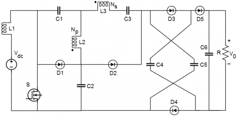
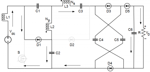
The operating principle of the suggested non-isolated positive output single-switch DC-DC converter topology shown in Figure 1 is analyzed based on the assumptions that: (i). The ideal models of active and passive elements are used in the converter; (ii). All inductors and capacitors are large enough so that no ripples appear in inductor currents and capacitor voltages. The continuous conduction mode operation of the proposed single-switch DC-DC converter is discussed under five different modes as shown below:
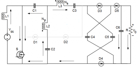
Mode I (t0<t<t1): The Mode I analysis of the converter is explained by means of Figure 2. During the time interval between t0 and t1, the MOSFET switch S is turned on and the diodes D3, D4, and D5 are under forward biased condition. The diodes D1 and D2 are under reverse biased condition. The current through the inductance L1 increases rapidly. The inductance L1 is charged to supply voltage Vdc. The parallel charging of capacitors C4, C5, and C6 occurs. The power is delivered to the load R from the source Vdc. This interval t0-t1 is a very small period. The current flow path for Mode I operation is shown in Figure 2.
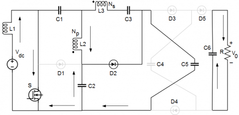
Mode II (t1<t<t2): The switch S continues to conduct and the diode D2 carries forward current during Mode II operation. The diodes D1, D3, D4, and D5 get open circuited. The stored energy in the capacitor C6 is delivered to the load R. The capacitor C2 charges the capacitor C1 and the inductor L2. The inductor L3 charges the capacitor C3. The capacitor C5 gets charged from the source. Whereas, the capacitor C4 gets disconnected from the source. The current flow path for Mode II operation is shown in Figure 3. The Mode II time interval is longer. The following Eqns. (1) and (2) are obtained for Mode II operation.
$\mathrm{V}_{\mathrm{L} 1}=\mathrm{V}_{\mathrm{dc}}$ (1)
$\mathrm{V}_{\mathrm{C} 3}=(\mathrm{n}+1)\left(\mathrm{V}_{\mathrm{C} 2}-\mathrm{V}_{\mathrm{Cl}}\right)$ (2)
where, ‘n’ represents the turns ratio (Ns / Np) of the coupled inductor. Ns = No. of turns in the windings of inductor L3. Np = No. of turns in the windings of inductor L2.
Figure 1. Proposed single-switch DC-DC converter configuration
Figure 2. Converter operation during Mode I
Figure 3. Converter operation during Mode II
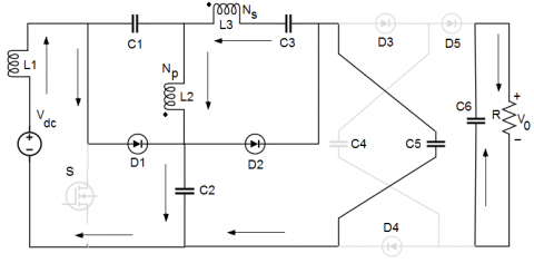
Figure 4. Converter operation during Mode III
Figure 5. Converter operation during Mode IV
Figure 6. Converter operation during Mode V
Mode III (t2<t<t3): During Mode III operation as depicted in Figure 4, the switch S is not conducting. The diodes D1 and D2 carry forward current. The diodes D3, D4, and D5 are under reverse biased condition. The capacitor C2 gets charged by the current through the inductor L1. The recycling of stored energy in the inductor L2 to the capacitor C1 occurs through the diode D1. The capacitor C5 gets charged from the source. Whereas, the capacitor C4 gets disconnected from the supply source. The load R receives energy from the capacitor C6. The Mode III interval is too small.
Mode IV (t3<t<t4): The Mode IV operation of the converter is explained as shown in Figure 5. During this time interval t3-t4, the switch S continues to maintain non-conducting state. The diodes D1, D3, D4 and D5 carry forward currents. The diode D2 is under reverse biased condition. During this interval, the source voltage charges the capacitors C4, C5, and C6 in parallel. The load R receives the power from the source. This interval t3-t4 is greater than that of Mode III. The following Eqns. (3) and (4) are obtained for Mode IV operation.
$\mathrm{V}_{\mathrm{L} 1}=\mathrm{V}_{\mathrm{dc}}-\mathrm{V}_{\mathrm{C} 2}$ (3)
$\mathrm{V}_{0}=\mathrm{V}_{\mathrm{C} 2}+\mathrm{V}_{\mathrm{L} 2}+\mathrm{V}_{\mathrm{L} 3}+\mathrm{V}_{\mathrm{C} 3}$ (4)
Mode V (t4<t<t5): During Mode V operation as shown in Figure 6, the switch S continues to remain turned off. The diodes D3, D4 and D5 carry forward currents. The diode D1 and D2 are under reverse biased condition. The source voltage charges the capacitors C4, C5, and C6 in parallel. The load R receives the power from the source through the diode D5. This interval t4-t5 is greater than that of Mode IV.
The following Eqns. (5) and (6) are obtained by applying the inductor volt-second balance principle and the voltage gain (G) of the proposed converter is obtained as shown in Eq. (7) by assuming the turns ratio (n) of the coupled inductor as 4.
$\mathrm{V}_{\mathrm{C} 1}=\frac{\mathrm{D}}{(1-\mathrm{D})} \mathrm{V}_{\mathrm{dc}}$ (5)
$\mathrm{V}_{\mathrm{C} 2}=\frac{1}{(1-\mathrm{D})} \mathrm{V}_{\mathrm{dc}}$ (6)
$\mathrm{G}=\frac{\mathrm{V}_{0}}{\mathrm{~V}_{\mathrm{dc}}}=\frac{6+5 \mathrm{D}}{(1-\mathrm{D})}$ (7)
where, D represents duty ratio of the switch S.
The above gain equation is obtained by assuming negligible leakage inductance and magnetizing inductance of the inductor.
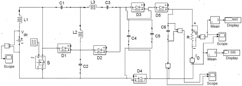
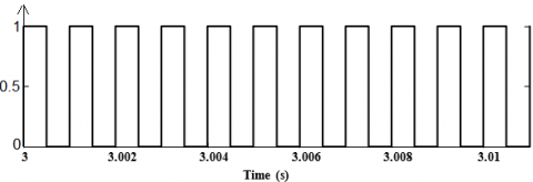
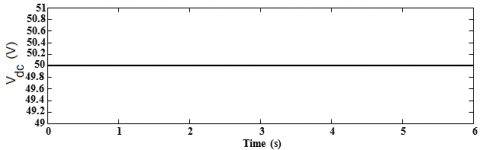
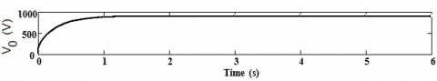
The MATLAB / SIMULINK model of the proposed non-isolated positive output single-switch DC-DC converter operating under continuous conduction mode is developed as shown in Figure 7 and simulated at a switching frequency of 1 kHz. The gate pulse given to the switch S is shown in Figure 8. Table 1 lists the values of parameters used for the simulation. The ‘ode 45’ solver with a graphical user interface (GUI) is used for the converter simulation. The performance of the converter is analyzed by varying the duty ratio D of the switch from 0.5 to 0.9. But, the waveforms for all active and passive elements are taken at low duty ratio (D = 0.5). At this low duty ratio itself, the load voltage (V0) of 900 V is obtained. Figure 9 indicates the input DC voltage of magnitude 50 V. The load voltage (V0) and load current (I0) are indicated as shown in Figure 10 and Figure 11 respectively. The waveforms of load voltage and load current reach the steady state without any overshoot and they have settling time of around 1 s. The voltage across the capacitors C4 and C6, and the resistive load R is same as V0.
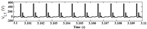
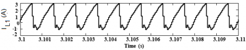
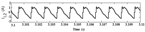
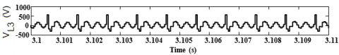
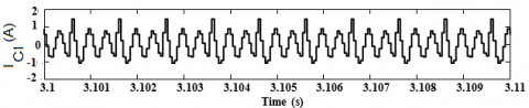
The capacitor C6 current is depicted as shown in Figure 12. This current is shown as a short pulse occurring for a very small interval of time. The capacitor C6 current is almost zero for about 1 ms duration following the peak instant. No ripples are found in the current and voltage waveforms of C6. The voltages waveforms for the inductors L1, L2, and L3 are shown in Figure 13 and Figure 16 respectively. The voltage across the inductors L1 and L2 reach peak value of around 500 V for a very short interval of time. Then the voltage decreases approximately to 190 V followed by very small fluctuations about 0 V axis. There are some fluctuations observed in the voltage waveform of L3 as shown in Figure 16 during the various modes of operation of the converter. At one instant, the voltage reaches the peak value of around 600V for very short interval of time and the voltage keeps on changing between positive and negative values. The three inductor current waveforms are shown in Figure 14, Figure 15, and Figure 17 respectively.
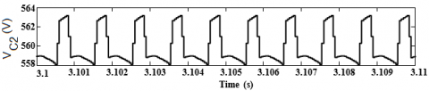
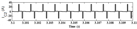
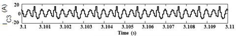
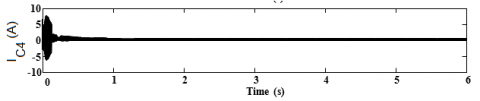
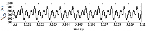
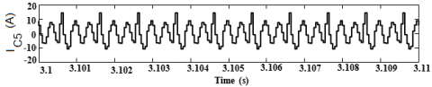
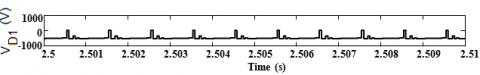
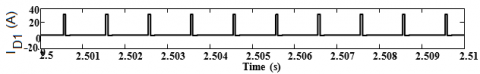
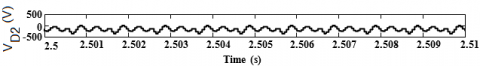
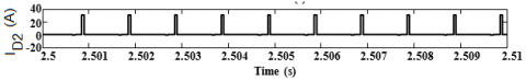
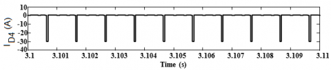
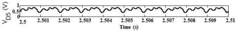
Similarly, all the capacitors’ (C1, C2, C3, C4, and C5) voltage waveforms are illustrated in Figure 18, Figure 20, Figure 22, and Figure 25 respectively, and the current waveforms for the same capacitors are shown in Figure 19, Figure 21, Figure 23, Figure 24, and Figure 26 respectively. Figure 27, Figure 29, Figure 31, and Figure 34 respectively illustrate the waveforms of voltages across the diodes D1, D2, D3, D4, and D5 respectively. From the Figure 27, it is understood that a negative voltage in the form of a short pulse appears across D1 for a very short interval of time followed by a constant negative voltage for the rest of the time. Then this pattern of voltage across D1 repeats. The Figure 29 and Figure 31 illustrate that the voltage pattern appearing across D2 and D3 keeps on varying in the negative direction. Whereas from Figure 34, it is clear that the voltage variation observed across D5 is between 0 V and 1 V only. Figure 28, Figure 30, Figure 32, Figure 33, and Figure 35 show the waveforms of currents through the diodes D1, D2, D3, D4, and D5 respectively. From the above Figures, it is understood that all the diodes D1, D2, D3, D4, and D5 carry currents in the form of a pulse for a very short duration followed by zero current instants. The diodes D1, D2, D3, and D5 carry positive currents and the diode D4 carries negative current.
Table 1. Parameters used for the converter simulation
|
Parameters |
Symbols |
Values |
|
Source voltage |
Vdc |
50 V (DC) |
|
Load voltage |
V0 |
900 V (DC) |
|
Load current |
I0 |
1.5 A (DC) |
|
Switching frequency |
fs |
1 kHz |
|
Inductors |
L1 |
66 µH |
|
L2 |
10 mH |
|
|
L3 |
110 µH |
|
|
Capacitors |
C1 |
360 µF |
|
C2 |
330 µF |
|
|
C3 |
110 µF |
|
|
C4, C5 |
40 µF each |
|
|
C6 |
3 mF |
|
|
Load Resistance |
R |
600 Ω |
|
Duty ratio of the MOSFET switch S |
D |
0.5 |
Figure 8. Gate pulse to the MOSFET switch S
Figure 9. Source voltage (Vdc) to the converter
Figure 10. Voltage (V0) at the load end of the converter
Figure 11. Current (I0) at the load end of the converter
Figure 12. Current through capacitor C6
Figure 13. Voltage across the inductor L1 and L2
Figure 14. Current through the inductor L1
Figure 15. Current through the inductor L2
Figure 16. Voltage across the inductor L3
Figure 17. Current through the inductor L3
Figure 18. Voltage across the capacitor C1
Figure 19. Current through the capacitor C1
Figure 20. Voltage across the capacitor C2
Figure 21. Current through the capacitor C2
Figure 22. Voltage across the capacitor C3
Figure 23. Current through the capacitor C3
Figure 24. Current through the capacitor C4
Figure 25. Voltage across the capacitor C5
Figure 26. Current through the capacitor C5
Figure 27. Voltage across the diode D1
Figure 28. Current through the diode D1
Figure 29. Voltage across the diode D2
Figure 30. Current through the diode D2
Figure 31. Voltage across the diodes D3 and D4
Figure 32. Current through the diode D3
Figure 33. Current through the diode D4
Figure 34. Voltage across the diode D5
Figure 35. Current through the diode D5
The steady state performance analysis of a non-isolated high gain positive output single-switch DC-DC converter structure with a voltage boosting module of diode-capacitor type is presented in this paper. The single-switch operation and the continuous input current are the features of the proposed converter. The low switch voltage-current stress and the reduced switching losses are the additional features of the converter. The voltage and current waveforms of all active and passive components are presented and analyzed. MATLAB / SIMULINK tool was used for simulating the converter and the results validate its performance. The results illustrate that the high gain capability of the suggested converter topology can be realized at low duty ratio (D = 0.5) itself. Further, no overshoot is observed in the load voltage and load current waveforms. However, the limitations of the converter suggested in this work are that (i). the number of passive elements and diodes used is more. (ii). the leakage inductance and magnetizing inductance for the coupled inductor are neglected to simplify the analysis. (iii). the turns ratio (n) of the coupled inductor is assumed as 4. The future research direction is towards the analysis of the proposed converter with definite values of leakage inductance and magnetizing inductance for the coupled inductor with turns ratio greater than four.
|
D |
Duty ratio of the switch S |
|
G |
Voltage gain of the proposed converter |
|
Vdc |
Input DC voltage (V) |
|
V0 |
Output voltage (V) |
|
I0 |
Output current (A) |
[1] Li, W., He, X. (2011). Review of nonisolated high-step-up DC/DC converters photovoltaic grid-connected applications. IEEE Transactions on Industrial Electronics, 58(4): 1239-1250. https://doi.org/10.1109/TIE.2010.2049715
[2] Gautam, D., Sharma, A.K., Shukla, J. (2019). A review of voltage boosting techniques for step-up DC-DC converter. International Journal of Innovative Research in Electrical, Electronics, Instrumentation and Control Engineering, 7(6): 35-41. https://doi.org/10.17148/IJIREEICE.2019.7607
[3] Tofoli, F.L., de Castro Pereira, D., de Paula, de Sousa Oliveira Júnior, D. (2015). Survey on non-isolated high-voltage step-up dc-dc topologies based on the boost converter. IET Power Electronics, 8(10): 2044-2057. https://doi.org/10.1049/iet-pel.2014.0605
[4] Forouzesh, M., Siwakoti, Y.P., Gorji, S.A., Blaabjerg, F., Lehman, B. (2017). Step-up dc-dc converters: A comprehensive review of voltage-boosting techniques, topologies, and applications. IEEE Transactions on Power Electronics, 32(12): 9143-9178. https://doi.org/10.1109/TPEL.2017.2652318
[5] Loera-Palomo, R., Morales-Saldana, J.A. (2015). Family of quadratic step-up dc-dc converters based on non-cascading structures. IET Power Electronics, 8(5): 793-801. https://doi.org/10.1049/iet-pel.2013.0879
[6] Chub, A., Vinnikov, D., Blaabjerg, F., Peng, F.Z. (2016). A review of galvanically isolated impedance-source DC-DC converters. IEEE Transactions on Power Electronics, 31(4): 2808-2828. https://doi.org/10.1109/TPEL.2015.2453128
[7] Shahir, F.M., Babaei, E., Farsadi, M. (2019). Extended topology for a boost dc-dc converter. IEEE Transactions on Power Electronics, 34(3): 2375-2384. https://doi.org/10.1109/TPEL.2018.2840683
[8] Dobi, A.H.M., Sahid, M.R. (2020). Non-isolated LLC resonant DC-DC converter with balanced rectifying current and stress. Indonesian Journal of Electrical Engineering and Computer Science, 18(2): 707-716. https://doi.org/10.11591/ijeecs.v18.i2.pp698-706
[9] Sowmya, A., Murali, D. (2019). A high voltage gain step-up resonant DC-DC converter topology with reduced switch count. International Journal for Modern Trends in Science and Technology, 5(12): 26-31. https://doi.org/10.46501/IJMTST051205
[10] Liang, T.J., Lee, J.H., Chen, S.M., Chen, J.F., Yang, L.S. (2013). Novel isolated high-step-up DC-DC converter with voltage lift. IEEE Transactions on Industrial Electronics, 60(4): 1483-1491. https://doi.org/10.1109/TIE.2011.2177789
[11] Divya Navamani, J., Vijayakumar, K., Jegatheesan, R. (2018). Non-isolated high gain DC-DC converter by quadratic boost converter and voltage multiplier cell. Ain Shams Engineering Journal (Electrical Engineering), 9(4): 1397-1406. https://doi.org/10.1016/j.asej.2016.09.007
[12] Revathi, S., Prabhakar, M. (2016). Transformerless high-gain dc-dc converter for microgrids. IET Power Electronics, 9(6): 1170-1179. https://doi.org/10.1049/iet-pel.2015.0406
[13] Muhammad, M., Armstrong, M., Elgendy, M.A. (2016). A nonisolated interleaved boost converter for high voltage gain applications. IEEE Journal of Emerging and Selected Topics in Power Electronics, 4(2): 352-362. https://doi.org/10.1109/JESTPE.2015.2488839
[14] Murali, D., Annapurani, S. (2019). A high voltage gain rectifier-fed two-stage step-up DC-DC converter with PI controller. International Journal of Engineering Applied Sciences and Technology, 4(8): 160-164. https://doi.org/10.33564/IJEAST.2019.v04i08.024
[15] He, P., Khaligh, A. (2017). Comprehensive analyses and comparison of 1 kW isolated DC-DC converters for bidirectional EV charging systems. IEEE Transactions on Transportation Electrification, 3(1): 147-156. https://doi.org/ 10.1109/TTE.2016.2630927
[16] Girija, V., Murali, D. (2021). Simulation and steady state analysis of a non-isolated diode rectifier-fed DC-DC boost converter with high static voltage gain. International Journal for Modern Trends in Science and Technology, 7(3): 20-25. https://doi.org/10.46501/IJMTST0703004
[17] Annapurani, S., Murali, D. (2020). Parallel-charge series-discharge inductor-based voltage boosting technique applied to a rectifier-fed positive output DC-DC converter. Journal of Applied Research and Technology, 18(5): 229-244. https://doi.org/10.22201/icat.24486736e.2020.18.5.1279
[18] Murali, D. (2021). Steady state behavior of a single-switch non-isolated DC-DC SEPIC converter topology with improved static voltage gain. Journal Européen des Systèmes Automatisés, 54(3): 445-452. https://doi.org/10.18280/jesa.540307
[19] Siwakoti, Y.P., Blaabjerg, F., Loh, P.C., Town, G.E. (2014). High-voltage boost quasi-Z-source isolated DC/DC converter. IET Power Electronics, 7(9): 2387-2395. https://doi.org/10.1049/iet-pel.2013.0845
[20] Babaei, E., Abbasi, F., Tarzamni, H., Kolahian, P. (2019). Isolated high step-up switched-boost DC/DC converter with modified control method. IET Power Electronics, 12(14): 3635-3645. https://doi.org/10.1049/iet-pel.2018.6114
[21] Nguyen, M.K., Duong, T.D., Lim, Y.C., Kim, Y.J. (2018). Isolated boost dc-dc converter with three switches. IEEE Transactions on Power Electronics, 33(2): 1389-1398. https://doi.org/10.1109/TPEL.2017.2679029
[22] Erickson, R.W., Maksimovic, D. (2001). Fundamentals of Power Electronics. Kluwer Academic Publishers, MA, USA, 39-55.
[23] Chincholkar, S.H., Jiang, W., Chan, C.Y. (2017). An improved PWM-based sliding-mode controller for a DC-DC cascade boost converter. IEEE Transactions on Circuits and Systems II: Express Briefs, 65(11): 1639-1643. https://doi.org/10.1109/TCSII.2017.2754292
[24] Lopez-Santos, O., Martinez-Salamero, L., Garcia, G., Valderrama-Blavi, H., Zambrano-Prada, D.A. (2017). Steady-state analysis of inductor conduction modes in the quadratic boost converter. IEEE Transactions on Power Electronics, 32(3): 2253-2264. https://doi.org/10.1109/TPEL.2016.2557582
[25] Yaramasu, V., Wu, B. (2011). Three-level boost converter based medium voltage megawatt PMSG wind energy conversion systems. Energy Conversion Congress and Exposition (ECCE), pp. 561-567. https://doi.org/10.1109/ECCE.2011.6063819
[26] Duarte, J., Lima, L., Oliveira, L., Mezaroba, M., Michels, L., Rech, C. (2013). Modeling and digital control of a single-stage step-up/down isolated PFC rectifier. IEEE Transactions on Industrial Informatics, 9(2): 1017-1028. https://doi.org/10.1109/TII.2012.2222039
[27] Evran, F., Aydemir, M.T. (2014). Isolated high step-up dc-dc converter with low voltage stress. IEEE Transactions on Power Electronics, 29(7): 3591-3603. https://doi.org/10.1109/TPEL.2013.2282813
[28] Qian, W., Cao, D., Cintron-Rivera, J.G., Gebben, M., Wey, D., Peng, F.Z. (2012). A switched-capacitor DC-DC converter with high voltage gain and reduced component rating and count. IEEE Transactions on Industrial Applications, 48(4): 1397-1406. https://doi.org/10.1109/TIA.2012.2199731
[29] Ajami, A., Ardi, H., Farakhor, A. (2015). A novel high step-up DC/DC converter based on integrating coupled inductor and switched-capacitor techniques for renewable energy applications. IEEE Transactions on Power Electronics, 30(8): 4255-4263. https://doi.org/10.1109/TPEL.2014.2360495
[30] Chen, S.M., Liang, T.J., Yang, L.S., Chen, J.F. (2013). A boost converter with capacitor multiplier and coupled inductor for AC module applications. IEEE Transactions on Industrial Electronics, 60(4): 1503-1511. https://doi.org/10.1109.TIE.2011.2169642
[31] Moradpour, R., Ardi, H., Tavakoli, A. (2017). Design and implementation of a new SEPIC-based high step-up DC/DC converter for renewable energy applications. IEEE Transactions on Industrial Electronics, 65(2): 1290-1297. https://doi.org/10.1109/TIE.2017.2733421
[32] Kim, H.Y., Moon, E.A., Nguyen, M.K. (2019). A novel negative-output high step-up ratio DC-DC converter based on switched-inductor cell. Journal of Institution of Korean Electrical and Electronics Engineering, 23(1): 273-279. https://doi.org/10.7471/ikeee.2019.23.1.273
[33] Ardi, H., Ajami, A., Sabahi, M. (2017). A SEPIC based high step-up DC-DC converter integrating coupled inductor for renewable energy applications. Proceedings of Power Electronics, Drive Systems & Technologies Conference (PEDSTC), pp. 206-211. https://doi.org/10.1109/PEDSTC.2017.7910324
[34] Chen, S.M., Lao, M.L., Hsieh, Y.H., Liang, T.J., Chen, K.H. (2015). A novel switched-coupled-inductor DC-DC step-up converter and its derivatives. IEEE Transactions on Industry Applications, 51(1): 309-314. https://doi.org/10.1109/TIA.2014.2332642
[35] Babaei, E., Saadatizadeh, Z. (2018). High voltage gain dc-dc converters based on coupled inductors. IET Power Electronics, 11(3): 434-452. https://doi.org/10.1049/iet-pel.2017.0051
[36] Santra, S.B., Chatterjee, D., Siwakoti, Y.P., Blaabjerg, F. (2021). Generalized switch current stress reduction technique for coupled-inductor-based single-switch high step-up boost converter. IEEE Journal of Emerging and Selected Topics in Power Electronics, 9(2): 1863-1875. https://doi.org/10.1109/JESTPE.2020.2998487
[37] Ardi, H., Ajami, A. (2018). Study on a high voltage gain SEPIC-based DC-DC converter with continuous input current for sustainable energy applications. IEEE Transactions on Industrial Electronics, 33(12): 10403-10409. https://doi.org/10.1109/TPEL.2018.2811123