Rahul Wilson Kotla* | Srinivasa Rao Yarlagadda
© 2021 IIETA. This article is published by IIETA and is licensed under the CC BY 4.0 license (http://creativecommons.org/licenses/by/4.0/).
OPEN ACCESS
Penetration of renewable energy systems (RES) into microgrid (MG) increases rapidly due to the intensified energy demands by the distribution level consumers. To meet this demand, consumers are erecting small scale distribution renewable energy generating systems (DREGS) which mostly constitutes of solar photovoltaic systems. Injecting power from the DREGS to the MG will rise potential problems like real and reactive power distortions, sag/swells which affect the power quality of the system. Voltage sags and swells are normally caused by MG intermittencies which occur at the high power and low energy situations. In order to maintain the power quality of the MG during intermittencies, an ultracapacitor (UC) is integrated along with a unified power quality conditioner (UPQC) with the DREGS is proposed in this paper. Basically, an ultracapacitor is a high power and low energy density device that will compensate the MG intermittencies. This proposed system deals with the control and design aspects of the ultracapacitor, a bidirectional converter for charging and discharging of UC, and a UPQC. The UPQC will act as a dynamic voltage restorer (DVR) for the MG side and an active power filter (APF) for the load side. The proposed system is designed and modelled using Matlab/Simulink platform and the results were analyzed.
Ultracapacitor, Unified power quality conditioner, Microgrid, Active power filter (APF), Dynamic voltage restorer (DVR)
Day to day power intake to the low voltage distribution grid or MG from all power generating sources was increasing and the fact that due to the modernization of all the industrial and home applications which are now majorly operated on electricity. All industrial loads which exist on the SPV linked MG’s will face power quality issues which causes system irregularities and stability problems [1]. DREGS export the excess power to the MG to satisfy the required demand. All DREGS come under non-conventional energy sources, out of which the SPV system is the major source. Due to this reason research mainly essences on SPV systems in recent years, and its design and modelling concepts were focused [2], [3] and some of the downsides of SPV are addressed to extract peak power from the system. For that MPPT algorithms are used for better yielding of output power [4], [5], [6].
However, the MG’s linked with the SPV systems generates power quality issues into MG due to the irregularities in neutral currents, unbalanced load currents, harmonics, and uneven sharing of real and reactive powers [7]. In weak MG’s due to the feed-in fluctuating SPV power into the MG will cause the voltage uncertainty problems like sags and swells [8], [9]. These voltage uncertainties will cause failures in power electronics systems due to false tripping of power electronic switches [10]. Power quality issues at the grid and consumer loads are serious issues at present-day MG’s. To overcome these power quality issues some of the suitable solutions are using a UPQC with the SPV interfaced grid linked inverter [11]. The main objective of designing a UPQC is to enhance the power quality in the MG’s by nullifying the harmonic currents caused by the sags, swells, and unbalanced loads.
A solar-powered versatile three-phase system is designed to recompense the load harmonics currents is discussed in [12]. A real power filtering mechanism in a single-phase solar-powered system is discussed in [13]. Mostly, single-phase and three-phase systems use shunt real power filter to work as a non-sinusoidal current source as discussed in [14], [15]. Series real power filters working as a non-sinusoidal voltage source which is tied between the MG and load can regulate the load unbalance voltages, reactive power of the load, and harmonic currents are discussed in [16]. It is well known that non-sinusoidal references are complicated to be analyzed using PWM converters, they require a further struggle to achieve decent real power filter performance, regarding this a dual compensation technique is employed in UPQC applications as discussed in [17].
Recent advancements in the power systems cause the penetration of DREGS like solar, wind, and plugin electric vehicles will give rise to power quality problems in the MG’s. Energy accumulating devices like the battery, UC, fuel cells, etc., installed with DREGS will be a possible solution for the power quality problems and decreases the uncertainties to maintain the reliable operation of the system [18]. In the upcoming years, integration of energy accumulating devices is crucial and is commercially implementing on a large scale for many applications [19]. In many DREGS, battery storage systems were integrated with the MG with different control techniques to mitigate the instabilities in the system [20],[21]. All the power quality problems due to intermittencies can be restored by using real power support as well as reactive power support from the energy accumulating devices. Out of all the available energy accumulating devices UCs is having the support for real power support for the MGs as well as reactive power support for the typical power distortion instances like voltage sags and swells [22].
This article addresses the power quality problems due to intermittencies in the DREGS tied MGs using UC based UPQC. The novelty of this paper is to introduce the UC with the UPQC device for the real power and reactive power assist to the MG and also presents the mathematical modelling of UC. Rather than the conventional battery-based DREGS tied low voltage MG’s, the proposed system selects a UC due to its higher charge/discharge cycles and more economical. The major advantage of the proposed topology is having an average current mode (ACM) control coordinated with a central level integrated controller (CLIC) for BDC, which will operate the BDC in a stable operating region. The rest of the paper organizes as follows, section 2 deals with the proposed system design of UC and bi-directional DC-DC converter (BDC), section 3 deals with the control strategy for threephase inverters of UPQC, a BDC, and a CLIC, section 4 presents the simulation outcomes of the proposed system and section 5 concludes the paper.
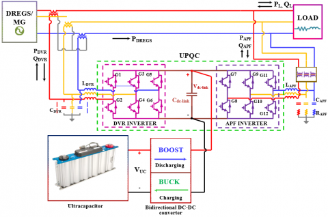
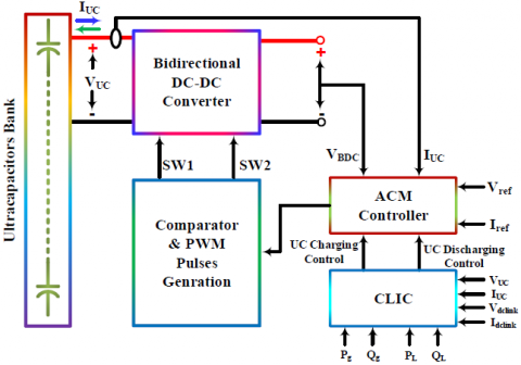
In this section, basic design concepts of UC and a BDC are discussed, and the proposed system block diagram is presented in Figure 1 and it shows that DREGS connected with the load and is controlled by a UPQC device. The UC is connected to the dc-link of the UPQC through a BDC as shown in Figure 1.
Figure 1. Block diagram of the proposed system with UC based UPQC
2.1 Design and modelling of ultracapacitor
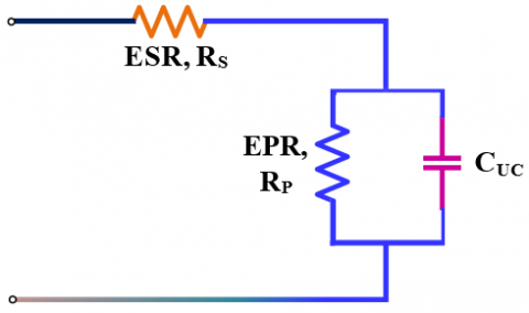
An ultracapacitor, also termed as an electrochemical capacitor or a supercapacitor, is an electrical energy storage device that is rapidly growing in popularity. The architecture and mechanism of operation are somewhere between a typical capacitor and a battery, which opens some exciting and useful applications. The equivalent circuit model of UC is shown in Figure 2, which constitutes of two resistors and a capacitor. The resistor which is parallel to the capacitor is called the equivalent parallel resistor (Rp), and the resistance which is series with the parallel combination of Rp and capacitor is called equivalent series resistor (Rs). Rp signifies the charging and discharging states of the UC and the Rs signifies the internal losses while the UC is in discharging mode.
Figure 2. Equivalent circuit of UC.
The key constraint that controls the value of UC capacitance is the value of the preferred standby time of the converter [23]. The energy stored in a UC depends on the variations in the voltage across its terminals and the capacitance of it, which can be given by eq. (1).
$E_{U C}=\frac{1}{2} C_{U C}\left(V_{i-U C}^{2}-V_{f-U C}^{2}\right)$ (1)
where,
EUC = Total capacity of energy that can be accumulated in the UC (W-sec)
Vi-UC = Voltage before discharging (V)
Vf-UC = Voltage after complete discharging (V)
CUC = UC capacitance (F)
The value of CUC can be calculated using eq. (2) [23] as follows
$C_{U C}=I_{U C-a v g} \times\left(\frac{1}{\Delta V}\right) \times \Delta t$ (2)
Usually, UC is discharged up to half of its rated capacity, at half of its rated capacity 1/3rd capacity of energy accumulated in the UC is discharged as stated in [23]. Beyond half of its rated capacity, it is not cost-effective to discharge the UC and its needs converter should be overrated. To avoid these drawbacks, while discharging it is better to choose the low voltage limit (VUC-low) as half of its rated voltage limit (VUC-rated) as given by eq. (3) [23].
$V_{U C-l o w}=\frac{V_{U C-r a t e d}}{2}$ (3)
The average current (Iavg) can be calculated using the following equations as stated in [23].
$I_{\max }=\frac{P_{\text {out }}}{V_{U C-l o w}}=2 \times \frac{P_{\text {out }}}{V_{U C-r a t e d}}$ (4)
$I_{\min }=\frac{P_{\text {out }}}{V_{U C-r a t e d}}$ (5)
From eq. (4) & (6), we can calculate the value of Iavg as
$I_{a v g}=\frac{I_{\max }+\mathrm{I}_{\min }}{2}=3 \times \frac{P_{\text {out }}}{V_{\text {UC}}- \text { rated }}$ (6)
where,
Pout = Converter power capacity at discharging
Imin =Minimum current of UC
Imax = Maximum current of UC
For a chosen value of converter rating, the minimum value of UC capacitance required is calculated as follows
$C_{U C-\min }=\frac{3 P_{out}}{V_{U C-r a t e d}^{2}} \quad \times \Delta t$ (7)
If the VUC is the voltage of a single UC around 2.5 V. For obtaining a higher voltage rating, the number of UCs should be connected in series and the total voltage rating of the seriesconnected UCs is given by eq. (8) and for obtaining the higher current rating, the number of UCs should be connected in parallel (p). For n and p connected UCs, the minimum value of capacitance (CUC-min) for a single UC is given by eq. (9).
$V_{U C-\text { series }}=n \times V_{U C}$ (8)
$C_{U C-m i n}=\frac{n \times C_{U C}}{p}$ (9)
where,
n = number of series connected UCs
VUC-series = Voltage across series connected UCs
p = number of parallel connected UCs
2.2 Design of Bidirectional DC-DC converter
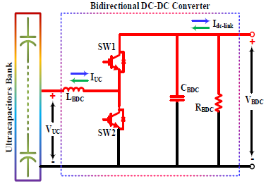
A Bidirectional DC-DC converter (BDC) is a buck-boost converter and it should be operated in three modes of operation. A BDC acts as an interface between the UC and the DC link to maintain the constant voltage at the DC link point even though the voltage of UC gets varied at the discharging mode. An UC based BDC is shown in Figure 3, in mode I the UC will be in discharging mode by providing the real and reactive power support as well as the voltage recovery during voltage sags. In mode II of BDC operation, the UC will be charged by taking the power from the DREGS/Grid by compensating for the intermittencies in the line. In mode III of operation, BDC will be in PWM blocking state where both switches are in the blocked state.
Figure 3. Ultracapacitors bank with bidirectional DC-DC converter
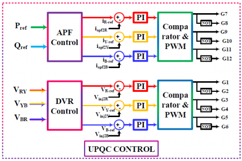
3.1 Control strategy for UPQC
The complete control strategy for UPQC is based on the controlling methods of DVR and APF inverters as shown in Figure 4. Two back-to-back three-phase inverters are connected through a dc-link capacitor in a UPQC topology as shown in Figure 1. One of the inverters acts as a series DVR which is connected between the DREGS and the dc-link capacitor and the other one is a shunt-connected APF inverter which is connected between the load and the dc-link capacitor. A BDC is connected to the dc-link capacitor to charge/discharge the UC storage of the proposed system. For DVR control, a PLL is used to estimate the value of angle θ, and the control method is known as the in-phase compensation method. The value of θ determines the voltages VRY, VYB, VBR, and these line-line voltages are transformed into the d-q components and the line to neutral voltages VRN, VYN, VBN can be approximated by using equation (10) as discussed in [24].
Figure 4. Control strategy for UPQC
$\left[\begin{array}{c}V_{R N} \\ V_{Y N} \\ V_{B N}\end{array}\right]=\left[\begin{array}{cc}1 & 0 \\ -\frac{1}{2} & \frac{\sqrt{3}}{2} \\ -\frac{1}{2} & -\frac{\sqrt{3}}{2}\end{array}\right]\left[\begin{array}{cc}\cos \left(\theta-\frac{\pi}{6}\right) & \sin \left(\theta-\frac{\pi}{6}\right) \\ -\sin \left(\theta-\frac{\pi}{6}\right) & \cos \left(\theta-\frac{\pi}{6}\right)\end{array}\right]\left[\begin{array}{c}\frac{V_{d}}{\sqrt{3}} \\ \frac{V_{q}}{\sqrt{3}}\end{array}\right]$ (10)
$\left[\begin{array}{c}V_{R-r e f} \\ V_{Y-r e f} \\ V_{B-r e f}\end{array}\right]=m \times\left[\begin{array}{c}\left(\sin \theta-\frac{V_{R N}}{V_{s}}\right) \\ \left(\sin \left(\theta-\frac{2 \pi}{3}\right)-\frac{V_{Y N}}{V_{s}}\right) \\ \left(\sin \left(\theta+\frac{2 \pi}{3}\right)-\frac{V_{B N}}{V_{s}}\right)\end{array}\right]$ (11)
These voltages are standardized using line to neutral voltage of 120 Vrms as a reference and equated with the actual system voltages Vs to identify the Vref. The real and reactive power supplied by DVR is obtained using equation (12) as follows,
$\left.\begin{array}{l}P_{D V R}=3 \times V_{i n j 2 R(r m s)} \times I_{L R(r m s)} \times \cos \phi \\ Q_{D V R}=3 \times V_{i n j 2 R(r m s)} \times I_{L R(r m s)} \times \sin \phi\end{array}\right\rangle$ (12)
where,
Vd = voltage at direct axis component
Vq = voltage at quadrature axis component
PDVR = real power of DVR
QDVR = reactive power of DVR
VR-Ref, VY-Ref, VB-Ref = Injected voltage references
Vs = actual system voltage
m = modulation index which is taken as 0.45
Vinj2R(rms) = rms values of injected voltage
ILR = Load current
ϕ = phase difference
The shunt/APF inverter is based on the d-q current compensation method(id-iq), in which iq is used to control the real power and id is used to control the reactive power. The d-q domain reference currents of APF inverter are calculated using equation (13), where Vq-s is the system voltage in q-axis and the current references are calculated using (14) as follows
$\left.\begin{array}{l}P_{A P F}=-\frac{3}{2} \times v_{q-s} \times i_{ref-q} \\ Q_{A P F}=-\frac{3}{2} \times v_{q-s} \times i_{r e f-d}\end{array}\right\rangle$ (13)
$\left[\begin{array}{c}i_{R-r e f} \\ i_{Y-r e f} \\ i_{B-r e f}\end{array}\right]=\left[\begin{array}{cc}1 & 0 \\ -\frac{1}{2} & \frac{\sqrt{3}}{2} \\ -\frac{1}{2} & -\frac{\sqrt{3}}{2}\end{array}\right]\left[\begin{array}{cc}\cos \theta & \sin \theta \\ -\sin \theta & \cos \theta\end{array}\right]\left[\begin{array}{l}i_{d-r e f }\\ i_{q-r e f}\end{array}\right]$ (14)
3.2 Control strategy for BDC
The voltage regulation of a BDC is done by using the ACM which is widely used in BDC controlling strategies [25], and a more stable operation is achieved to control the BDC for charging and discharging purposes of UC. The UC based APF has discharged the energy when the voltage reference Vref value is greater than the Vout-BDC value, which operates the BDC in boost mode by making the Iuc-ref current flow positive, and for the buck mode of operation, Vref value is lesser than the Vout-BDC value thereby making the Iuc-ref current flow negative. The ACM control and the CLIC are shown in Figure 5.
Figure 5. Control strategy for BDC along with the CLIC
3.3 Central level integrated controller
The CLIC controls the BDC and the UPQC circuit based on the circuit parameters like real and reactive powers of the grid (Pg, Qg), load (PL, QL), voltage and current of UC (VUC, IUC) and dc-link (Vdc-link, Idc-link) as shown in Figure 5. This CLIC will operate in 5 states based on the above parametric inputs. In state I, CLIC will operate as a real power assist state and in state II it will operate as a DREGS intermittency smoothing state. In the state I and state II of operation the real power values PL, Pg is used to set the Pref value to control the UCBDC system for supplying real power to the grid, and the Pref will decide that whether the system should be operated in grid assist mode or UC charge mode. In state III, CLIC will operate in a reactive power assist state, in this state UC-BDC system will supply the reactive power to the grid, and the BDC losses will be supplied by the grid. In state III the reactive power values QL, Qg is used to set the Qref value to control the UCBDC system for supplying reactive power to the grid, and the Qref will operate the BDC to maintain a constant dc-link voltage.
In state IV, the CLIC will set the BDC to operates in boost mode to discharge the UC to compensate for the sag/swell instabilities for a short duration. Whenever there are shortterm disturbances exist on the line, the energy stored in the UC should be supplied for a short duration to overcome these types of disturbances in the system. At the time of swell, the BDC should absorb the additional real power caused by the swell to stabilize the system, and at the time of sag, it should supply the real power to meet the requirement of the system. In state IV, the CLIC will set the BDC to operates in buck mode to charge the UC, when its state of charge comes below half of its total capacity.
The simulation circuit of the proposed system is shown in Figure 6, and the simulation parameters are shown in Table. 1. The proposed system is designed and developed in Matlab / Simulink platform.
Figure 6. Simulation circuit of the proposed system
Table 1. Simulation parameters of the proposed system
|
Sl. No |
Parameter |
Value |
|
1 |
DREGS/Grid Voltage, Vg |
208 V |
|
2 |
Capacitance of UC, CUC |
60 F |
|
3 |
Input inductance of BDC, LBDC |
160 μF |
|
4 |
Output capacitance of BDC, CBDC |
45 μF |
|
5 |
Output resistance of BDC, Rout |
215 Ω |
|
6 |
DC link capacitance, Cdc-link |
3600 μF |
|
7 |
DVR series inductance, LDVR |
1.5 mH |
|
8 |
APF series inductance, LAPF |
1.5 mH |
|
9 |
DVR shunt capacitance, CDVR |
100 μF |
|
10 |
APF shunt capacitance, CAPF |
100 μF |
|
11 |
Frequency |
50 Hz |
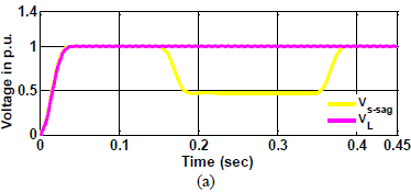
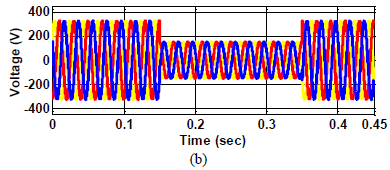
For the case I, the proposed system response is obtained in per unit values as shown in Figure 7(a), and for obtaining the three-phase system response the sag voltage of source in rms (Vs-sag) is induced in the system from time, t = 0.15 sec to 0.35 sec and the extent of the sag is taken up to 0.47 p.u. During sag, the load voltage (VL) will be remained constant at around 0.99 p.u. with the help of UPQC. The line-to-line source voltages (VSRY, VSYB, VSBR) of DREGS/grid is shown in Figure 7(b) and is having a voltage dip from 0.15 sec to 0.35 sec. This voltage dip is compensated by using a UPQC device with the help of UC-BDC, the injected voltages (Vinj2R, Vinj2Y, Vinj2B) is shown in Figure 7(c). During Vs-sag, the additional voltage required by the load is supplied by the UPQC to keep the line-to-line Load voltages (VLRY, VLYB, VLBR) as constant as shown in Figure 7(d).
Figure 7. Voltage sag condition is taken from 0.15 sec to 0.35 sec (a) Vs-sag and VL in p.u. (b) the line to line source voltages (c) injected voltages of UPQC (d) line to line load voltages
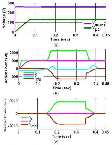
During voltage sag, Figure 8(a) presents the voltage of a BDC, Figure 8(b) and Figure 8(c) presents the real and reactive powers of the DREGS/grid, load, and UPQC. From Figure 8, during voltage sag, the real power deficit from the DREGS/grid is compensated by the UPQC device, which is the same as the input power of the inverter which was taken from UC storage. It is also identified that during sag the reactive power from DREGS/grid is reduced and it is compensated using reactive power supplied by the UPQC. The proposed system's real and reactive power support is simulated using Figure 8. During the time, t = 0 to 0.225 sec, the system operates in reactive power assist mode using reactive power from the UPQC which is shown in Figure 8(c), from 0.225 sec to 0.45 sec, the system operates in real power assist mode. The voltages of UC and the dc-link side are shown in Figure 8(a) and the real and reactive powers of the proposed system are shown in Figure 8(b) and Figure 8(c).
Figure 8. Sag condition. (a) Voltages of BDC and UC. (b) Real and Reactive powers of the proposed system using UPQC
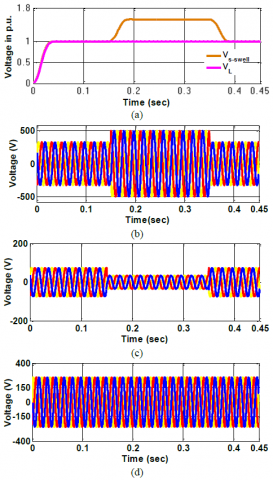
For case II, the proposed system response is obtained in per unit values as shown in Figure 9(a), and for obtaining the three-phase system response the swell voltage of source in rms (Vs-swell) is induced in the system from time, t = 0.15 sec to 0.35 sec and the extent of the sag is taken up to 0.53 p.u. During sag, the load voltage (VL) will be remained constant at around 0.99 p.u. with the help of UPQC. The line-to-line source voltages (VSRY, VSYB, VSBR) of DREGS/grid is shown in Figure 9(b) and is having voltage dip from 0.15 sec to 0.35 sec. This voltage dip is compensated by using a UPQC device with the help of UC-BDC, the injected voltages (Vinj2R, Vinj2Y, Vinj2B) is shown in Figure 9(c). During Vs-sag, the additional voltage required by the load is supplied by the UPQC to keep the line-to-line Load voltages (VLRY, VLYB, VLBR) as constant as shown in Figure 9(d).
Figure 9. Voltage swell condition is taken from 0.15 sec to 0.35 sec. (a) Vs-swell and VL in p.u. (b) the line to line source voltages (c) injected voltages of UPQC (d) line to line load voltages
During voltage swell, Figure 10(a) presents the voltage of a BDC, Figure 10(b) and Figure 10(c) presents the real and reactive powers of the DREGS/grid, load, and UPQC. From Figure 10, during voltage swell the surplus real power from the DREGS/grid is taken by the UPQC device, to charge the UC storage. The proposed system's real and reactive power are shown in Figure 10. The voltages of UC and the dc-link side are shown in Figure 10(a) and the real and reactive powers of the proposed system are shown in Figure 10(b) and Figure 10(c).
Figure 10. Swell condition. (a) Voltages of BDC and UC. (b) Real and Reactive powers of the proposed system using UPQC
In this article, the proposed system uses an ultracapacitor based BDC converter and UPQC between the DREGS and loads to improve the power quality in the MG system. The voltage sag and swell will be compensated using the DVR portion of the UPQC. The real and reactive power assist will be provided by the APF portion of the UPQC to overcome the intermittencies caused by the disturbances. A CLIC integrated ACM control is employed to regulate the BDC converter to maintain the constant dc-link voltage. The DVR inverter employs an in-phase compensation control technique and the APF uses a current control d-q technique to control the proposed system are discussed. From the simulation results, it is clear that the proposed system performs well to compensate for the short-term disturbances in the Microgrids.
[1] Basit, M. A., Mathe, L., Dilshad, S., Badar, R., Sami ur Rehman, S. M. (2020). Limitations, challenges, and solution approaches in grid-connected renewable energy systems. International Journal of Energy Research, 1–31. DOI: 10.1002/er.5033
[2] Kotla, R.W., Yarlagadda, S.R. (2020). Mathematical modelling of SPV array by considering the parasitic effects. SN Applied Sciences, 2:50. https://doi.org/10.1007/s42452-019-1861-x
[3] Kotla, R.W., Yarlagadda, S.R. (2020). Modelling and Control of a Three Phase PVGT System. IEEE India Council International Subsections Conference (INDISCON), pp. 96-101, https://doi.org/10.1109/INDISCON50162.2020.00031.
[4] Wilson, K.R., Rao, Y.S. (2019). Comparative Analysis of MPPTT Algorithms for PV Grid Tied Systems: A Review. In 2nd IEEE International Conference on Intelligent Computing, Instrumentation and Control Technologies (ICICICT), 1: 1105-1110.
[5] Kotla, R.W., Yarlagadda, S.R. (2020). Grid tied solar photovoltaic power plants with constant power injection maximum power point tracking algorithm. Journal Européen des Systèmes Automatisés, 53(4): 567-573. https://doi.org/10.18280/jesa.530416
[6] Kotla, R.W., Yarlagadda, S.R. (2021). A Novel enhanced active power control maximum power point tracking algorithm for photovoltaic grid tied systems. Advances in Electrical and Computer Engineering, 21(3): 81-90. https://doi.org/ 10.4316/AECE.2021.03010
[7] Francisco, C., Rosa, D.L. (2015). Harmonics, power systems, and smart grids. 2nd ed. Boca Raton, FL: CRC Press. https://doi.org/10.1201/9781315215174
[8] Parchure, A., Tyler, S.J., Peskin, M.A., Rahimi, K., Broadwater, R.P., Dilek, M. (2017). Investigating pv generation induced voltage volatility for customers sharing a distribution service transformer. IEEE Transanctions on Industry Applications, 53(1): 71–79.
[9] Kotla, R.W., Yarlagadda, S.R. (2021). Power Management of PV-Battery-Based Low Voltage Microgrid Under Dynamic Loading Conditions. Journal of The Institution of Engineers (India): Series B, 102(4): 797-806. https://doi.org/ 10.1007/s40031-021-00544-2
[10] Singh, B., Chandra, A., Haddad, K. A. (2015). Power quality: problems and mitigation techniques. London: Wiley.
[11] Anzalchi, A., Sarwat, A. (2017). Overview of technical specifications for grid-connected photovoltaic systems. Energy Conversion and Management, 152: 312-327. https://doi.org/10.1016/j.enconman.2017.09.049
[12] Agarwal, R.K., Hussain, I., Singh, B. (2017). Three- phase single-stage grid tied solar pv ecs using PLL-less fast CTF control technique. IET Power Electronics, 10(2): 178–188.
[13] Singh, Y., Hussain, I., Singh, B., Mishra, S. (2017). Single-phase solar gridinterfaced system with active filtering using adaptive linear combiner filter-based control scheme. IET Generation, Transmission Distribution, 11(8): 1976–1984.
[14] Rao, Y.S., Pathak, M.K. (2020). Model predictive control for three-level cascaded H-bridge D-STATCOM. IETE Journal of Research, 66(1): 65-76, DOI: 10.1080/03772063.2018.1476189
[15] Campanhol, L.B.G., Silva, S.A.O., Goedtel, A. (2014). Application of shunt active power filter for harmonic reduction and reactive power compensation in three- phase four-wire systems. IET Power Electronics, 7(11): 2825–2836.
[16] Salmeron, P., Litran, S.P. (2010). Improvement of the electric power quality using series active and shunt passive filters. IEEE Transanctions on Power Electronics. 25(2): 1058-1067.
[17] Modesto, R.A., Silva, S.A.O., Oliveira, A.A. (2015). Power quality improvement using a dual unified power quality conditioner/uninterruptible power supply in three-phase four-wire systems. IET Power Electronics, 8(3): 1595-1605.
[18] Ribeiro, P.F., Johnson, B.K., Crow, M.L., Arsoy, A., Liu, Y. (2001). Energy storage systems for advanced power applications. Proc. IEEE, 89(12): 1744–1756.
[19] Rittershausen J. McDonagh, M. (2020). Moving energy storage from concept to reality: southern California edison’s approach to evaluating energy storage [Online]. Available:http://www.edison.com/content/dam/eix/docu ments/innovation/smart-grids/Energy-Storage-Concept- toReality-Edison.pdf
[20] Tant, J., Geth, F., Six, D., Tant, P., Driesen, J. (2013). Multiobjective battery storage to improve PV integration in residential distribution grids. IEEE Transactions on Sustainable Energy, 4(1): 182–191.
[21] Brekken, T.K.A., Yokochi, A., Jouanne, A.V., Yen, Z.Z., Hapke H.M., Halamay, D.A. (2011). Optimal energy storage sizing and control for wind power applications. IEEE Transactions on Sustainable Energy, 2(1): 69–77.
[22] Das, S.R., Ray, P.K., Mohanty, A., Singh, V.P., Mishra,
A.K. (2020). Improvement in power quality using ultra- capacitor-integrated hybrid-active filter for current harmonic mitigation. In Computing Algorithms with Applications in Engineering, 139-149.
[23] Naresh, P., Kishore, N.S.V., Kumar, V.S.S., (2020). Mathematical modeling and stability analysis of an ultracapacitor based energy storage system considering non-idealities. Journal of Energy Storage, 102112. https://doi.org/10.1016/ j.est.2020.102112.
[24] Akagi, H., Watanabe, E.H., Aredes, M. (2007). Instantaneous Reactive Power Theory and Applications to Power Conditioning. 1st ed. Hoboken, NJ, USA: Wiley/IEEE Press.
[25] Erickson, R.W., Maksimovic, D. (2001). Fundamentals of Power Electronics. 2nd ed. Norwell, MA, USA: Kluwer.