Israa Mohammed Rasheed*![]() | Hassan Jassim Motlak
| Hassan Jassim Motlak![]()
© 2024 The authors. This article is published by IIETA and is licensed under the CC BY 4.0 license (http://creativecommons.org/licenses/by/4.0/).
OPEN ACCESS
The growing need for high-performance folded cascode CMOS OTAs in various fields, such as electronics and communications, requires them to operate with wide bandwidth, high voltage gain, compact devices, and low power consumption. Recent research indicates that implementing the water cycle algorithm (WCA) can greatly improve the performance of the folded cascode CMOS operational transconductance amplifier (OTA). This is due to the WCA's ability to perform both global search and local exploration efficiently. Notably, the OTA in question is constructed using 0.18µm TSMC technology and operates with a voltage supply of ±1.8V. The results of the simulation were collected using PSPICE software (version 17.4). These design solutions demonstrate exceptional efficiency, delivering significant amplification, high frequency, and minimal power usage. In addition, the paper demonstrates the implementation and simulation outcomes of a folded cascode CMOS operational transconductance amplifier utilizing the water cycle algorithm, MATLAB was employed for this purpose. Using WCA in the design of an OTA for folded cascode CMOS OTA results in significant improvements in performance metrics. Experiences a significant increase in voltage gain, with an increase in gain bandwidth by a factor of five compared to the algorithm-free design. In addition, power consumption is reduced by 15.5%, and the common mode rejection ratio is improved by 15.18% compared to the non-WCA folded cascode CMOS OTA design. The results highlight the effectiveness of the WCA technique as a powerful optimization strategy to improve the performance of folded cascode CMOS OTA.
water cycle algorithm, CMOS folded cascode, operational transconductance amplifier, OTA, power consumption, gain bandwidth, voltage gain, phase margin, and slew rate
Using operational amplifiers has become increasingly important in analog circuit design due to their high gain and direct connection. Typically, they consist of a level transistor, a differential amplifier stage, and an output stage [1]. The prevalence of Complementary Metal-Oxide Semiconductor (CMOS) technology over bipolar technology in analog circuit design for mixed signal systems is primarily driven by the industry's inclination to integrate analog and digital circuits on a single chip utilizing common process technologies [2]. Modern technologies that reduce the size of the transistor provide many benefits and advantages needed by many applications. Among these benefits are increased integration density, reduced energy consumption, as well as improved performance, in addition to cost efficiency and other benefits.
Digital CMOS technology manufactures the majority of analog integrated circuits. Over the years, the efficiency of digital CMOS circuits has enhanced due to advancements in digital technology. Digital technology has consistently reduced the minimal feature size, enabling the construction of digital circuits with smaller dimensions, increased speed, and reduced parasitic effects. However, manufacturers continue to manufacture analog circuits with greater channel lengths to optimize circuit performance [3]. Scalability is a characteristic of digital circuits, which allows for the adaptation of the same circuit to a more advanced technology over time with minimal modifications. However, while transitioning from an older to a newer technology in analog circuits, it is necessary to reconfigure the aspect ratios of most transistors in order to preserve the desired performance.
Several designs of CMOS op-amps can be found in Accepted Manuscript literature, all of which aim to optimize their performance parameters. Genetic algorithm, particle swarm optimization, simplex-PSO, modified cuckoo optimization algorithm, hybrid whale particle swarm optimization, aging leader and challenger PSO (ALC-PSO), and colliding bodies optimization (CBO) are just some of the methods utilized to optimize the dimensions of each transistor and enhance the performance of op-amps for design the analog and mixed-signal integrated circuit [4-11]. The improvements reported in more research papers demonstrate that certain performance parameters have been enhanced. However, it is evident that other parameters still require further optimization.
The key challenge in this design is to strike a balance between the various performance metrics, such as gain, bandwidth, noise, power consumption, and linearity, while ensuring the OTA can function effectively in high-frequency domains. Careful transistor sizing, biasing techniques, compensation methods, and other circuit design strategies may be employed to address this challenge and further improve the overall performance of the folded-cascode CMOS OTA.
In this paper, the WCA algorithm was employed to enhance the performance characteristics of the proposed folded cascode CMOS OTA. The performance of the folded cascode CMOS OTA was compared with and without the WCA algorithm. The simulation results indicated that the proposed design developed using the WCA method exhibited superior performance parameters, thus demonstrating the effectiveness of the WCA algorithm.
This circuit amplifier consists of two types of cascode CMOS OTAS. The first one is the telescopic cascode CMOS OTA which is realized using one-stage input differential pair MOS transistors and a tail current transistor which connected in series with two legs of cascoding MOS transistors to increase the output impedance of OTA [12]. This will improve DC voltage gain, output impedance, slew rate, and settling time of OTA. This technique suffers from the limitation on the output voltage swings and input voltage common-mode range due to cascoding MOS transistors in series with the input differential pair MOS transistors [13]. The second type of cascode CMOS OTA is the folded cascode CMOS OTA as shown in Figure 1. The configuration of this technique uses input differential pair MOS transistors and output folded cascoding MOS transistors [14]. The steps to design of folded cascode CMOS OTA are shown in the following points [15, 16].
Figure 1. Schematic of folded cascode CMOS OTA circuit diagram [16]
$S R=I_3 / C_L$ (1)
$I_5=I_4=1.2 I_3$ to $1.5 I_3$ (2)
$\begin{gathered}S_5=2 I_5 / K_P V_{D S 5}^2, S_7=\frac{2 I_7}{K_P V_{D S 7}^2},\left(S_4=S_5 \& S_6=S_7\right) \\ V_{D S 5(\text {sat})}=V_{D S 7(\text {sat})}=0.5\left(V_{D D}-V_{\text {out }(\text {max})}\right)\end{gathered}$ (3)
$\begin{gathered}S_{11}=\frac{2 I_{11}}{K_N V_{D S 11}^2}, S_9=\frac{2 I_9}{K_N V_{D S 9}^2},\left(S_{10}=S_{11} \& S_8=S_9\right) \\ V_{D S 9(\text {sat})}=V_{\text {DS11(sat})}=0.5\left(V_{\text {out }(\text {min})}-V_{S S}\right)\end{gathered}$ (4)
$(\mathrm{GB})=\frac{g_{m 1}}{C_L}, S_1=S_2=\frac{g_{m 1}^2}{K_N I_3}=G B^2 C_L^2 / K_N I_3$ (5)
$S_3=\frac{2 I_3}{K_N\left(V_{\text {in(min})}-V_{S S}-\sqrt{\frac{I_3}{K_N S_1}}-V_{\text {th } 1}\right)^2}$ (6)
$S_4=S_5=2 * \frac{I_4}{K_P\left\{V_{D D}-V_{\text {in (max})}+V_{t h 1}\right\}^2}$ (7)
$S_4$ and $S_5$ must satisfy or surpass the specified value of step Eq. (3).
$\mathrm{P}_{\text {diss }}=\left(V_{D D}-V_{S S}\right)\left(I_3+I_{10}+I_{11}\right)$ (8)
$\begin{gathered}A V=\frac{V_{\text {out }}}{V_{\text {in }}}=\left(\frac{2+K}{2+2 K}\right) g_{m 1} R_{I I} \\ K=\frac{R_9\left(g_{d s 2}+g_{d s 4}\right)}{g_{m 7} r_{d s 7}}, R_9=g_{m 9} r_{d s 9} r_{d s 11} \\ R_{I I}=R_9 \|\left[g_{m 7} r_{d s 7}\left(r_{d s 2} \| r_{d s 5}\right)\right]\end{gathered}$ (9)
$V_{\text {PB1 }}=V_{\text {DD }}-\left(V_{\text {OD5 }}+V_{\text {th } 5}\right)$ (10)
$\mathrm{V}_{\mathrm{PB} 2}=\mathrm{V}_{\mathrm{DD}}\left(\left|\mathrm{V}_{\mathrm{GS} 3}\right|+\left|\mathrm{V}_{\mathrm{OD} 5}\right|\right)$ (11)
The input differential MOS transistors are connected to a tail current source MOS transistor. This topology is very suitable for high input common-mode voltage range, high output swings, large voltage gain Av, high gain bandwidth product (GB), and large slew rate (SR) due to the cancellation of extra phase shift that is required by the second stage of the conventional two stages CMOS OTA.
One of the phenomena that occur in nature is the water movement between rivers and streams towards the ocean. This phenomenon is called the water cycle [17]. River water, water resulting from the photosynthesis of plants, melting snow, groundwater, and rainwater resulting from the evaporation of river and lake water, all collect in the sea in a sequence of states called the water cycle as in Figure 2 and its flow chart in Figure 3. While in Table 1, the parameters of input for the optimization process are outlined.
Figure 2. A simplified schematic illustrating the hydrologic cycle (water cycle) [18]
Figure 3. Flowchart of WCA [19]
Table 1. Parameters of WCA
|
No. |
INPUTS Algorithm Parameter |
Value |
Parameter Definition |
|
1 |
Nvars |
3 |
Number of design variables |
|
2 |
Npop |
200 |
Population size |
|
3 |
Nsr |
8 |
Number of rivers + sea |
|
4 |
dmax |
1e-20 |
Evporation condition constant |
|
5 |
Max_it |
1000 |
Maximum number of iterations |
The WCA initial population consists of raindrops that occur during rain or precipitation. A single raindrop is considered to be a part of the sea. The valuable rains symbolize the rivers. The residual raindrops are the tributaries that flow into the rivers and, ultimately, the ocean.
A single solution or a raindrop of the optimization problem in WCA terms is represented by a $1 \times N_{v a r}$ dimensional array, as specified below [20]:
Raindrop $=\left[X_1, X_2, \ldots, X_{N_{\text {var }}}\right]$ (12)
The optimization problem dimension is $N_{\text {var}}$.
The raindrop cost functions (Cost) is determined by:
Cost $_i=\int\left(X_1, X_2, \ldots, X_{N_{v a r}}\right), i=1,2, \ldots, N_{\text {pop }}$ (13)
where, the raindrop counts is stored in $N_{\text {pop}}$.
The direction of rainwater flow, whether it goes into the sea or rivers, is determined by the equation, which takes into account the intensity of the flow:
$\begin{gathered}N S_n= { round }\left\{\left|\frac{\operatorname{Cost}_n}{\sum_{i=1}^{N_{s r}} \operatorname{Cost}_i}\right| * N_{ {Raindrops }}\right\}, \\ n=1,2, \ldots, N_{s r}\end{gathered}$ (14)
where, $N_{s r}$ is the single sea and river's total number. $N_{\text {Raindrops }}$refers to the remaining portion of the population, specifically those raindrops that fall directly into the sea or rivers.
$N_{ {Raindrops }}=N_{ {pop }}-N_{s r}$ (15)
The raindrops give rise to the formation of streams. The streams serve as tributaries that give rise to rivers or directly discharge into the ocean. The sea, being the most optimal destination, serves as the final terminus for all streams and rivers. The assessment of the new location for the rivers and streams is conducted by:
$X_{ {Stream }}^{i+}=X_{ {Stream }}^i+$ rand $* C *\left(X_{ {River }}^i-X_{ {stream }}^i\right)$ (16)
$X_{ {River }}^{i+}=X_{ {River }}^i+$ rand $* C *\left(X_{ {Sea }}^i-X_{ {River }}^i\right)$ (17)
Assuming that C is a variable that can assume values between 1 and 2, and rand is a uniformly distributed random number between 0 and 1.
The roles of the stream and the river can be reversed if the solution presented by the stream is more effective than the solution represented by the river. Similarly, the sea and the rivers can also interchange their roles. The parameter dmax has a significant influence on determining whether further exploration around the sea, which represents the best solution, should be promoted or discouraged [21]:
$d_{\max }^{i+1}=d_{\text {max }}^i-\frac{d_{\max }^i}{\text { Iter_max }}$ (18)
Precipitation follows the process of evaporation. The formation of new streams occurs when fresh raindrops accumulate in certain designated locations:
$X_{\text {stream }}^{\text {new }}=L B+$ rand $*(U B-L B)$ (19)
In the given problem, the upper and lower limits of the search parameters are denoted by UB (Upper Bound) and LB (Lower Bound), respectively. These limits define the range within which the search algorithm explores and evaluates potential solutions.
To ensure accurate representation and analysis of the folded cascode CMOS OTA, several design parameters and specifications are outlined in Tables 2 and 3, respectively. Table 2 presents the design parameters, encompassing various aspects such as supply voltage, bias currents, and capacitor values. Channel length and channel width (transistor dimensions) play an important role in improving performance parameters. The focus of the design appears to be on a folded-cascode CMOS Operational Transconductance Amplifier (OTA) targeted for high-frequency applications. These high-frequency applications may include Analog-to-Digital Converters (ADCs), Digital-to-Analog Converters (DACs), universal filters, and other circuits that operate at elevated frequencies [22].
Table 2. Folded cascode CMOS OTA specifications
|
Design Parameters |
Values with Units |
|
Voltage Gain |
>70 dB |
|
Gain Bandwidth |
>40MHz |
|
Slew Rate |
>35V/µsec |
|
Supply Voltage $(V D D, V S S)$ |
±1.8V |
|
Input Common Mod Range |
-0.95 to +1 V |
|
Phase Margin |
≥ 55 ° |
|
Load Capacitor |
0.5pF |
|
I bias |
25uA |
Table 3. Folded cascode CMOS OTA aspect ratios of transistors for designed with and without WC
|
Number of Transistor |
Gate Width (µm) W |
Gate Width (µm) W (WCA) |
Channel Length L (µm) |
|
W1,2 |
0.725 |
29.53 |
0.18 |
|
W3,12 |
1.008 |
0.3474 |
0.18 |
|
W4,5 |
3.75 |
3.708 |
0.18 |
|
W6,7 |
2.435 |
2.17 |
0.18 |
|
W8,9,10,12 |
0.845 |
0.752 |
0.18 |
In order to utilize the WCA for optimization in MATLAB, it is necessary to incorporate the parameters to be optimized into the fitness equation, as depicted in Eq. (20). The WCA performs a predetermined number of iterations as specified by the user. The findings generated by the WCA can be utilized in the PSPICE program to assess the performance metrics of the Folded Cascode CMOS OTA. These criteria include minimum power consumption, gain bandwidth, voltage gain, and common mode rejection ratio (CMRR). This iterative procedure can be reiterated until the desired result of reduced power consumption, elevated voltage amplification, and enhanced gain bandwidth is attained while upholding a consistent bias current. Using these optimized parameter values, the transistors can be redesigned with enlarged dimensions. Integrating the WCA with the Folded Cascode CMOS OTA optimization allows for systematic design refinement and the achievement of higher performance. The synergy between the WCA and the PSPICE program facilitates the evaluation and refinement of the Op-Amp's performance parameters, leading to the identification of optimal transistor dimensions that result in enhanced overall circuit performance.
Fitness function $=\frac{\left(\frac{1}{\mathrm{Pdiss}}+G B\right)-\left(\text { Pdiss }+\frac{1}{G B}\right)}{2}$ (20)
Table 3 shows detailed information about the dimensions of the transistor used in the design. By based on the process parameters in Table 2 and using the Eq. (1) to Eq. (6), we can found the aspect ratio of all transistors as in Table 3, Such tables have an important role in configuring and evaluating the performance of folded cascode CMOS OTA, as they are considered a reference point for accurate evaluation using SPICE simulation.
Once the WCA optimization process is completed using the MATLAB (R2021b) program, improved results for performance parameters are obtained. The three parameters $\left(S_1, V_{D S}\right.$, and $\left.\mathrm{X}\right)$ are found by algorithm, and by based on these values, we can find all parameters as shown:
$\mathrm{S}_{1,2}=164.07 \Rightarrow \mathrm{w}_{1,2}=0.18 * 164.07=29.53 \mu \mathrm{m}$
$\mathrm{x}=1.2$, $\mathrm{x}$ is the ratio of current in $\mathrm{M}_{4,5}\left(\mathrm{I}_{4,5}\right)$ to bias current $I_3$ in Eq. (2):
$V_{D S}=0.185 \mathrm{~V}$, where $V_{D S}=V_{D S 5}=V_{D S 7}=V_{D S 9}$
where, $S_{1,2}, V_{D S}$, and $x$ are found by the algorithm. And by based on these values, we can find all parameters as follow:
$\begin{gathered}\mathrm{I}_5=\mathrm{I}_4=1.2 \mathrm{I}_3 \text { to } 1.5 \mathrm{I}_3=\mathrm{x} * 25=1.201 * 25=30.025 \mu \mathrm{A} \\ \mathrm{I}_7=\mathrm{I}_{4,5}-\mathrm{I}_{1,2}=30.025-12.5=17.525 \mu \mathrm{A}\end{gathered}$
$\begin{gathered}\mathrm{GB}=\frac{\sqrt{\mathrm{S}_{1,2} * \mathrm{~K}_{\mathrm{N}} \mathrm{I}_3}}{\mathrm{C}_{\mathrm{L}}}=\frac{\sqrt{164.07 * 245 * 10^{-6} * 25 * 10^{-6}}}{2 \pi * 0.5 * 10^{-12}}=319.1 \mathrm{MHZ}\end{gathered}$
$\begin{gathered}\mathrm{S}_3=\frac{2 * 25 * 10^{-6}}{245 * 10^{-6}\left(-0.95+1.8-\sqrt{\frac{25 * 10^{-6}}{245 * 10^{-6} * 164.07}}-0.5\right)^2} \\ =1.93 \Rightarrow \mathrm{W}_3=0.18 * 1.93=0.3474 \mu \mathrm{m}\end{gathered}$
$\begin{gathered}\mathrm{S}_{4,5}=\frac{2 * 30.025 * 10^{-6}}{85 * 10^{-6} * 0.185^2}=20.6 \Rightarrow \mathrm{W}_{4,5}=0.18 * 20.6 =3.708\end{gathered}$
$\begin{gathered}\mathrm{S}_{6,7}=\frac{2 * 17.525 * 10^{-6}}{85 * 10^{-6} * 0.185^2}=12.05 \Rightarrow \mathrm{W}_{6,7}=0.18 * 13.53 =2.17 \mu \mathrm{m}\end{gathered}$
$\begin{gathered}\mathrm{S}_{8,9,10,11}=\frac{2 * 17.525 * 10^{-6}}{245 * 10^{-6} * 0.185^2}=4.18 \Rightarrow \mathrm{W}_{8,9,10,11} =0.18 * 4.18=0.752 \mu \mathrm{m}\end{gathered}$
$\begin{gathered}\mathrm{S}_{4,5}=\frac{30.025 * 10^{-6}}{85 * 10^{-6}(1.8-1+0.5)^2}=0.272 \ll 20.6 \\ \mathrm{P}_{\text {diss }}=3.6 *(25+17.525+17.525) * 10^{-6}=216.18 \mu \mathrm{W} \\ \mathrm{AV}=\frac{\mathrm{V}_{\text {out }}}{\mathrm{V}_{\text {in }}}=\left(\frac{2+\mathrm{K}}{2+2 \mathrm{~K}}\right) \mathrm{g}_{\mathrm{m} 1} \mathrm{R}_{\mathrm{II}}\end{gathered}$
$\begin{gathered}\mathrm{g}_{\mathrm{m} 9}=\sqrt{2 * \mathrm{I}_9 * \mathrm{~K}_{\mathrm{N}} * \mathrm{~S}_{\mathrm{g}}}=\frac{189.5 \mu \mathrm{A}}{\mathrm{V}} \Rightarrow \mathrm{R}_9=\mathrm{r}_{\mathrm{ds} 9} \mathrm{r}_{\mathrm{ds} 11}=385.3 \mathrm{M} \Omega \\ \mathrm{g}_{\mathrm{m} 7}=\sqrt{2 * \mathrm{I}_7 * \mathrm{~K}_{\mathrm{p}} * \mathrm{~S}_7}=\frac{189.5 \mu \mathrm{A}}{\mathrm{V}} \\ \mathrm{K}=\frac{385.3 * 10^6\left(\frac{1}{2 * 10^6}+\frac{1}{0.66 * 10^6}\right)}{189.5 * 10^{-6} * 1.14 * 10^6}=3.59\end{gathered}$
$\begin{aligned} & \mathrm{R}_{\mathrm{II}}=385.3 * 10^6 \|\left[189.5 * 10^{-6} * 1.14 * 10^6\right. \left.*\left(2 * 10^6 \| 0.66 * 10^6\right)\right]=83.868 * 10^6 \Omega\end{aligned}$
$\begin{gathered}\mathrm{AV}=\frac{2+3.59}{2+2 * 3.59} * 1002.45 * 10^{-6} * 83.868 * 10^6 =51195.07 * 10^6=94.18 \mathrm{~dB} \\ \text { Area }=\sum=0.18 * 10^{-6} *(29.53 * 2+0.3474 * 2+3.708 * 2+2.17 * 2+0.752 * 4)=13.4 \mu \mathrm{m}^2\end{gathered}$
The folded cascode CMOS OTA was designed using the water cycle algorithm and gave great results compared to other sources that rely on the use of algorithms for optimization. In addition, a fixed amount of current was relied upon, estimated at 25µA, and also a load capacity of 0.5 square meters.
Figures 4-8 respectively present the simulation results for gain bandwidth, phase margin, slew rate (SR), settling time (St), and CMRR of the basic folded cascode CMOS OTA before and after using WCA. These illustrations offer a clear understanding of the folded cascode CMOS OTA's performance attributes and operational tendencies. Also, these figures showcase the performance enhancements achieved through the optimization process.
By comparing these results with the corresponding figures obtained before utilizing the water cycle algorithm, the impact of the optimization process on the folded cascode CMOS OTA's performance parameters becomes apparent. Table 4 delivers a detailed comparison of the main performance parameters for both scenarios: with and without the WCA implementation, as well as benchmarking against references employing various algorithms.
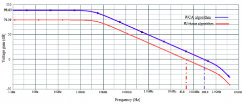
Figure 4. Simulation results for gain bandwidth (with and without WCA algorithm)
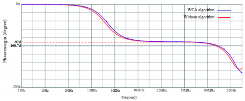
Figure 5. Simulation results for phase margin (with and without WCA algorithm)
Figure 6. Simulation results for transconductance (with and without WCA algorithm)
Figure 7. Simulation results for settling time (St) and slew rate measurement (with and without WCA algorithm)
(a) Diffrenetial mode
(b) Common mode
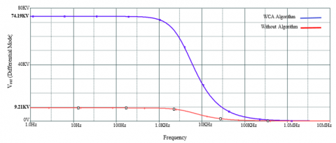
Figure 8. Simulation results of CMRR (a), (b) (with and without WCA algorithm)
Table 4. The performance parameters of the folded cascode CMOS OTA with and without WCA, as well as with other reference designs
|
Performance Parameters |
Theoretical Results |
WCA |
HWPSO [8] |
MCOA [23] |
MRFC [24] |
|
DC Gain (dB) |
79.29 |
98.63 |
56.11 |
53.9 |
76.24 |
|
Gain Bandwidth (MHz) |
47.8 |
300.5 |
0.55 |
398 |
74.7 |
|
Slew Rate(V/mS) |
48.05 |
49.68 |
15.07 |
470 |
64.05 |
|
Settling time (ns) |
38.11 |
35.3 |
----- |
------- |
---- |
|
CMRR (dB) |
126.26 |
142.62 |
74.48 |
----- |
----- |
|
Power dissipation (mW) |
255.6 |
216 |
6.106 |
1100 |
540 |
|
Phase margin (degree) |
88 |
79.3 |
---- |
62.9 |
74.406 |
|
Area(mm2) |
3.46 |
14.3 |
21 |
128 |
2760 |
|
Transconductance(mA/V) |
144 |
919 |
----- |
------- |
---- |
|
Technology |
0.18 |
0.18 |
0.18 |
0.18 |
0.18 |
|
Temperature (℃) |
27 |
27 |
27 |
27 |
27 |
The performance parameters of the proposed folded cascode CMOS OTA are affected by the load capacitance (CL), which is demonstrated in Table 5. It is observed that when the value of CL (load capacitance) decreases:
Figures 4 to 8 demonstrate that the voltage gain achieved with the WCA is 98.63 dB, representing a 24.4% increase compared to the previous value of 79.29 dB without utilizing the WCA. In the study [8], the voltage gain is reported as 56.11 dB, while in the study [22], it is stated as 53.9 dB. Additionally, the gain bandwidth (GB) is significantly improved with the WCA, reaching 300.5 MHz, which is improve the previous value of 47.8 MHz. In the study [8], the GB is reported as 0.55 MHz, while in reference [23], it is stated as 74.7. The power dissipation of the optimized design is reduced by 15.5%, decreasing from 255.6 μW to 216 μW after applying the WCA. In the study [8], the power dissipation is reported as 6.106 μW, while in the study [22], it is noted as 1100 μW and in the study [23], it is state as 540 μW. Moreover, other parameters such as CMRR and settling time (ts) also exhibit improvements through the use of the Water Cycle Algorithm, For temperature influence, this design is room temperatures and note the results are among the acceptable Ring compared to other research as in Table 4.
Table 5. The performance parameters of the proposed folded cascode CMOS OTA according to influence of load capacitance (CL)
|
With (WCA) |
||||
|
CL(pF) |
DC Gain(dB) |
GB(MHZ) |
Phase Margin |
Settling Time(ns) |
|
10 |
98.63 |
16.26 |
89.4 |
464.9 |
|
8 |
98.63 |
20 |
89.25 |
368.8 |
|
6 |
98.63 |
27.13 |
89 |
276.4 |
|
4 |
98.63 |
40.8 |
88.4 |
184.4 |
|
2 |
98.63 |
81.5 |
86.9 |
92.2 |
|
1 |
98.63 |
162.6 |
83.75 |
44.7 |
|
0.5 |
98.63 |
300.5 |
79.3 |
35.3 |
|
Without WCA |
||||
|
10 |
79.29 |
2.6 |
90 |
692.81 |
|
8 |
79.29 |
3.2 |
89.9 |
547.51 |
|
6 |
79.29 |
4.3 |
89.85 |
413.5 |
|
4 |
79.29 |
6.4 |
89.78 |
273.81 |
|
2 |
79.29 |
13.08 |
89.54 |
134.1 |
|
1 |
79.29 |
26.1 |
89.08 |
67.13 |
|
0.5 |
79.29 |
47.8 |
88 |
38.11 |
Upon comparing all the results, it becomes evident that the WCA outperforms other types of algorithms in terms of achieving superior performance parameters for the folded cascode CMOS OTA. The significant enhancements observed in voltage gain, GB, area, phase margin, CMRR, and settling time validate the effectiveness of the water cycle Algorithm for optimizing the proposed design.
The continuous advancements in integrated circuit manufacturing have led to remarkable improvements in transistor performance. By conducting simulations using PSPICE (version 17.4) and based on 180nm TSMC technology, several key findings have been concluded:
[1] Sabry, M.N., Nashaat, I., Omran, H. (2020). Automated design and optimization flow for fully-differential switched capacitor amplifiers using recycling folded cascode OTA. Microelectronics Journal, 101: 104814. https://doi.org/10.1016/j.mejo.2020.104814
[2] Rezaei, I., Soldoozy, A., Zanjani, M.S., Aghaee, T. (2023). Recycling folded cascode two-stage CMOS amplifier. Memories-Materials, Devices, Circuits and Systems, 6: 100093. https://doi.org/10.1016/j.memori.2023.100093
[3] Kalita, D. (2020). Design of PMOS and NMOS input folded cascode amplifier using 180nm SCL technology node for low power application. International Journal of Innovative Technology and Exploring Engineering, 9(4): 1372-1375. https://doi.org/10.35940/ijitee.D1624.029420
[4] Nakhaei, R., Mallahzadeh, A., Operational, A.S.B.O.O. (2012). Transconductance amplifier using an evolutionary algorithm. Australian Journal of Basic and Applied Sciences, 2012: 88-96.
[5] Faragó, C., Lodin, A., Groza, R. (2014). An operational transconductance amplifier sizing methodology with genetic algorithm-based optimization. Acta Technica Napocensis. Electronica-Telecomunicatii, 55(1): 15.
[6] Maji, K.B., Kar, R., Mandal, D., Ghoshal, S.P. (2016). An evolutionary approach based design automation of low power CMOS two-stage comparator and folded cascode OTA. AEU-International Journal of Electronics and Communications, 70(4): 398-408. https://doi.org/10.1016/j.aeue.2015.12.019
[7] Anisheh, S.M., Dadkhah, C. (2017). A two-stage method for optimizing the parameters of CMOS operational amplifiers based on evolutionary algorithm. International Journal on Computer Science and Engineering, 14(2): 1-10.
[8] Laskar, N.M., Guha, K., Nath, S., Baishnab, K.L., Paul, P.K. (2020). Optimal sizing of recycling folded cascode amplifier for low-frequency applications using new hybrid swarm intelligence-based technique. Applied Artificial Intelligence, 34(12): 880-897. https://doi.org/10.1080/08839514.2020.1790163
[9] Motlak, H.J., Mohammed, M.J. (2019). Design of self-biased folded cascode CMOS op-amp using PSO algorithm for low-power applications. International Journal of Electronics Letters, 7(1): 85-94. https://doi.org/10.1080/21681724.2018.1440422
[10] De, B.P., Kar, R., Mandal, D., Ghoshal, S.P. (2016). An efficient design of CMOS comparator and folded cascode op-amp circuits using particle swarm optimization with an aging leader and challengers algorithm. International Journal of Machine Learning and Cybernetics, 7: 325-344. https://doi.org/10.1007/s13042-015-0412-z
[11] De, B.P., Kar, R., Mandal, D., Ghoshal, S.P. (2016). Soft computing-based approach for optimal design of on-chip comparator and folded-cascode op-amp using colliding bodies optimization. International Journal of Numerical Modelling: Electronic Networks, Devices and Fields, 29(5): 873-896. https://doi.org/10.1002/jnm.2152
[12] Chan, P.K., Ng, L.S., Siek, L., Lau, K.T. (2001). Designing CMOS folded-cascode operational amplifier with flicker noise minimisation. Microelectronics Journal, 32(1): 69-73 https://doi.org/10.1016/S0026-2692(00)00105-1
[13] Feizbakhsh, S.V., Yosefi, G. (2019). An enhanced fast slew rate recycling folded cascode Op-Amp with general improvement in 180 nm CMOS process. AEU-International Journal of Electronics and Communications, 101: 200-217. https://doi.org/10.1016/j.aeue.2019.01.021
[14] Rasheed, I.M., Motlak, H.J. (2023). Performance parameters optimization of CMOS analog signal processing circuits based on smart algorithms. Bulletin of Electrical Engineering and Informatics, 12(1): 149-157. https://doi.org/10.11591/eei. v12i1.4128
[15] Manideep, I., Kumar, D.V. (2016). A 2.5 GHz CMOS folded cascode operational amplifier. Development, 3(8): 131-135.
[16] Koonapalli, H., Ramakrishnan, V.N. (2020). Design of radiation hardened complementary folded cascode amplifier. Materials Today: Proceedings, 24: 1766-1776. https://doi.org/10.1016/j.matpr.2020.03.601
[17] Sadollah, A., Eskandar, H., Lee, H.M., Yoo, D.G., Kim, J.H. (2016). Water cycle algorithm: A detailed standard code. SoftwareX, 5: 37-43.
[18] Eskandar, H., Sadollah, A., Bahreininejad, A., Hamdi, M. (2012). Water cycle algorithm–A novel metaheuristic optimization method for solving constrained engineering optimization problems. Computers & Structures, 110: 151-166. https://doi.org/10.1016/j.compstruc.2012.07.010
[19] Hussien, A.G., Hashim, F.A., Qaddoura, R., Abualigah, L., Pop, A. (2022). An enhanced evaporation rate water-cycle algorithm for global optimization. Processes, 10(11): 2254. https://doi.org/10.3390/pr10112254
[20] Roeva, O., Angelova, M., Zoteva, D., Pencheva, T. (2020). Water cycle algorithm for modelling of fermentation processes. Processes, 8(8): 920. https://doi.org/10.3390/pr8080920
[21] Sadollah, A., Yoo, D.G., Yazdi, J., Kim, J.H., Choi, Y. (2014). Application of water cycle algorithm for optimal cost design of water distribution systems. In 11th International Conference on Hydroinformatics, New York City, USA, pp. 1-8.
[22] Kumngern, M., Khateb, F., Kulej, T., Knobnob, B. (2024). 1 V tunable high-quality universal filter using multiple-input operational transconductance amplifiers. Sensors, 24(10): 3013. https://doi.org/10.3390/s24103013
[23] Anisheh, S.M., Dadkhah, C. (2017). A two-stage method for optimizing the parameters of CMOS operational amplifiers based on evolutionary algorithm. International Journal on Computer Science and Engineering, 14(2): 1-10.
[24] Venishetty, S.R., Sundaram, K. (2019). Modified recycling folded cascode OTA with enhancement in transconductance and output impedance. Turkish Journal of Electrical Engineering and Computer Sciences, 27(6): 4472-4485. https://doi.org/10.3906/elk-1902-82