Performance Comparison of Si and GaAs Solar Cell due to Deposition of ZnO and SiO2 Antireflection Coating Layer

Jhilirani Nayak*![]() | Priyabrata Pattanaik
| Priyabrata Pattanaik![]() | Dilip Kumar Mishra
| Dilip Kumar Mishra![]()
© 2024 The authors. This article is published by IIETA and is licensed under the CC BY 4.0 license (http://creativecommons.org/licenses/by/4.0/).
OPEN ACCESS
This article provides a new approach to the comparison of the performance of low-cost, efficient, and stable silicon and gallium arsenide solar cells. The design convention becomes challenging due to the absorption and current mismatching of the used antireflection coating layer with device sub-layers. The electrical properties of the proposed devices were analyzed in the presence of zinc oxide and silicon dioxide anti-reflection coating (ARC) layer, by adopting COMSOL 5.6 simulation software. These monolithically designed single junction solar cells of distinct materials with various band gaps and diverse spectral characteristics furnish the best efficiency with impressive degradation in reflection losses. The wideband antireflection layers are used to reduce reflection losses by reducing the refractive index towards the top surface of the photovoltaic cells. Simulation results provide the optimized values of the parameters of the devices within the range of 200-1200nm wavelength. At a thickness of 0.5µm zinc oxide, silicon solar cell and gallium arsenide solar cell provides efficiency of 16.85% and 10.69% respectively. Deposition of silicon dioxide on zinc oxide enhances the power efficiency to 16.89% and 10.7% respectively. A set of figures including maximum voltage, maximum current, conversion efficiency, short circuit current, and fill factor are presented. This article represents the use of zinc oxide and silicon dioxide antireflection layers with their optimum thickness can provide a better improvement in the device's performance.
anti-reflection collating layer, current mismatch, efficiency, reflectivity, band gap and fill factor, COMSOL 5.6 simulation, zinc oxide, silicon dioxide, photovoltaic cells
An excellent fidelity and economical price made the single junction solar cell dominant for future use [1, 2]. Single junction solar cells are contemplated as the first-generation solar cells. These solar cells are expensive to fabricate as finding pure and elemental structures of silicon materials is very challenging. So, researchers deviated their research towards second-generation solar cells. Thin film semiconductor materials have characterized the framework of second-generation solar cells. These cells have environmental controversies and their performances are comparatively lower. Moving towards the third-generation solar cell, which uses less advanced technology commercially. They can suppress the Shockley-Queisser limit [3]. Shockley’s limit states the procedure to calculate maximum conversion efficiency theoretically for a pn-junction solar cell. Maximum efficiency was calculated and restricted to 30% at 1.1eV because of radiative recombination loss. In the field of photovoltaic cells, the Shockely-Queisser limit is one of the most significant achievements. The computation was done with a 6000K black body spectrum which was approximately comparable to the solar spectrum. Subsequent computation with solar spectra AM 1.5 yields an efficiency of 33.16% for a single junction solar cell at a band gap of 1.34eV.
Silicon solar cells outcomes a maximum power efficiency of 32% because of their lower band gap of 1.1eV. Reflection of the front part of the photovoltaic cell and light obstruction of the surface thin wires restrain the efficiency to 24% for commercial mono-crystalline solar cells. Shockely-Quessier limit is applied only to a conventional single pn-junction solar cell. In the extreme limit, solar cells of higher than one junction with an immense number of layers provide an efficiency limit of 68.7% under traditional sunlight and 86.8% under concentrated light.
Multijunction photovoltaic cells, solar cells with numerous absorption paths, intermediate energy level solar cells, and photovoltaic cells based on hot carriers are the objectives behind developing third-generation solar cells. A classic part of solar cell research is to improve conversion efficiency. If materials are taken into consideration, then silicon will be considered as the dominant over other materials with a very good efficiency. Along with silicon, gallium arsenide cells also receive attention because of their high-power conversion efficiency [4-6]. Even with improved conversion efficiency, their performance is still below the theoretical limit due to the reflection losses. Reflection losses are more than 30% in the case of silicon and 35% in gallium arsenide [7, 8]. A considerable amount of antireflection techniques was introduced to reduce the effect of the reflection. These techniques are imperative elements to put down losses due to Fresnel reflection. As a result, there will be a step up in the amount of light entering the solar cell, obviously upgrading the conversion efficiency. With the progress in photovoltaic technology, the urge for good antireflection coatings also rises [9].
To alleviate the effect of Fresnel reflective losses, a single-layer antireflection coating, and a double-layer anti-reflection coating were adopted [10-14]. These coating techniques impart impressive performance over a certain width of the wavelength. Results based on the experimental study of antireflection coatings state that silicon solar cells with TiO2 antireflection coating enhance the efficiency by up to 14.27% in comparison to 11.24% without the antireflection coating [15]. According to Swatowska et al. [16], a conversion efficiency of 9.84% was achieved for crystalline silicon solar cells without the deposition of antireflection coating, and 14% and 14.25% were attained by depositing TiO2 and Si3N4 antireflection coatings. A separate survey by Gee et al. [17] states, that subsequently an efficiency of 15.55% and 16.03% was achieved from crystalline silicon solar cells by covering it with TiO2 and ZnO antireflection coating. It yields that out of various numbers of ARCs, ZnO would be an earmark choice. Besides that, modeling a solar cell including an ARC is a crucial task because of using umpteen choices in parameters and materials. A taste of modification in any feature of ARC fabrication is challenging and valuable. Nowadays, the first simulation was carried out before going for fabrication [18].
A survey conveys that silicon solar cell with 5nm SiO2 antireflection coating provides an efficiency of 4.72%, a double-layer antireflection coating of SiO2/Si3N4 bring forth an efficiency of 4.56% using Silvaco ATLAS [19-21]. Another software PC1D came up with an efficiency of 10.78% using TiO2, 11.7% using ZnO, and 11.89% using Si3N4 single-layer antireflection coating-based silicon solar cell. But the aforementioned solar cell with a double layer of ZnO/TiO2 and SiO2/TiO2 raises efficiency up to 13.37% 1nd 13.59%. According to Naser et al. [22], 18% and 19% efficient solar cells of silicon materials can be obtained with zinc oxide and zinc sulfide antireflection coating layer. An enhancement of 6.7% in the short circuit current has been crystalline silicon solar cells when coated with Si3N4 and SiO2 anti-reflection coating [21, 23]. Also, GaAs solar cells demonstrate an optimum short-circuit current at a thickness of 65nm of the ZnO layer and 80nm of the MnO layer [22, 24]. Research states that software like PC1D, MATLAB, and Silvaco ATLAS design, optimize, and analyze photovoltaic cells with antireflection coatings. Here we have adopted another software i.e., COMSOL Multiphysics in which the input parameters can be varied stepwise to investigate the output parameters.
In the presented paper, we have contrived the solar cell build-up of silicon and gallium arsenide materials coated with a zinc oxide and silicon dioxide anti-reflection coating layer. The devices were simulated at a thickness of 0.5µm of SiO2 and ZnO and calibrated. The work also focuses on efficiency, short circuit current, maximum current and fill factor of the device with and without anti-reflection coating layer. Considering wavelengths range from 200nm to 1200nm, the simulated devices present better achievements of the used ARC layers over the solar cell. The study's purpose and objectives are to design and compare the efficiency of the proposed solar cells.
2.1 Solar cells without antireflection coating
Characterization was done to measure the I-V and P-V characteristics of solar cells. The one-dimensional model of the silicon and gallium arsenide solar cell has been simulated and characterized here. According to the constructional view, it consists of anti-reflection coating layers and distinct sub-layers. For the single junction cell, optimized antireflection coatings are used to prevent large losses of incident light due to surface reflection. The devices were designed, and simulated by using COMSOL multiphysics version 5.6 and optimized.
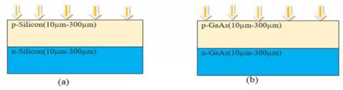
To simulate the silicon solar cell, its structure consists of an N-type silicon wafer with an area of 1×1cm2 and an optimum thickness of 150µm. For the gallium arsenide, a thickness of 80µm has been selected. To do a better result analysis, the thickness was varied from 10µm to 300µm. The cell structure contains a pn-junction with 1×1018cm-3 doping concentration for P-type and 1×1015cm-3 doping concentration for N-type. The aforementioned device was analytically doped with uniform doping of concentration at the bottom and geometrically doped with a concentration of P-type as a front surface doping. As a part of the assumption, the doping was uniform in both layers. The schematic of the solar cell structure is given in the Figure 1.
Figure 1. Structures of (a) Silicon solar cell and (b) Gallium arsenide solar cell
2.2 Solar cells with antireflection coating
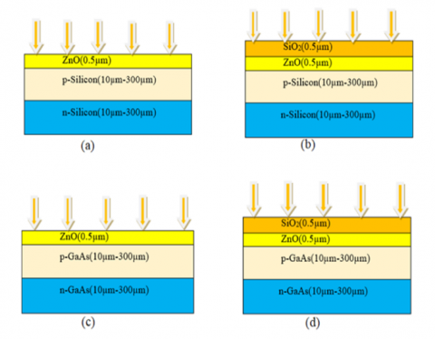
The front surface was optically coated with zinc oxide and silicon dioxide to investigate the device under the effect of antireflection coating. It is shown in Figure 2. The characterization of the device was done understand the effect of two antireflection coating layers. The refractive index and thickness were varied to inspect the different properties of the device in the presence of two antireflection layers. The antireflection layers' thickness was evaluated using the standard equation, given by Solanki [25].
$t=\frac{\lambda}{4 n_1}$ (1)
The refractive index $n^{\wedge}(\lambda)$ of the antireflection coating materials is complex and defined as the function of wavelength. The equation represents this complex refractive index in [18], where $n(\lambda)$ is the real part and $i k(\lambda)$ is the imaginary part.
$\boldsymbol{n}^{\wedge}(\lambda)=\boldsymbol{n}(\lambda)+i k(\lambda)$ (2)
The minimum reflection is given by the study [25]:
$R_{\text {min }}=\frac{\left(n_1^2-n_0 n_2\right)}{\left(n_1^2+n_0 n_2\right)}$ (3)
where, $n_0, n_1$ and $n_2$ are the refractive indices of air, antireflection coatings, and semiconductors.
Figure 2. Structures of (a) Silicon solar cell with ZnO, (b) Silicon solar cell with ZnO and SiO2, (c) Gallium arsenide solar cell with ZnO and (d) Gallium arsenide solar cell with ZnO andSiO2
The major impact of antireflection coating is to maximize the short-circuit current Isc. The short-circuit current is represented by the study [1]:
$I_{S C}=\frac{q}{A} \int \frac{I(\lambda)}{E(\lambda)}(1-R(\lambda)) \operatorname{IQE}(\lambda) d \lambda$ (4)
where A represents the area of cross-section, q represents elementary electric charge, I(λ) is irradiance, E(λ) is the energy of the photon, IQE(λ) is the internal quantum efficiency of the cell and R(λ) is the reflection coefficient of the incident light energy (or reflectance). The anti-reflection coating has to be optimized so that the current produced in the cell should be optimum. Eqs. (1), (3) and (4) were used for the calculation of thickness, minimum reflection and short-circuit current of the antireflection layers.
The electrical parameters that were used in the simulation with their numerical values are mentioned in the given Table 1.
Table 1. Electrical parameters of silicon and gallium arsenide solar cell
|
Parameters |
Values |
||
|
Silicon (Si) |
Gallium Arsenide (GaAs) |
Zinc Oxide (ZnO) |
|
|
Bandgap |
1.12(eV) |
1.424(eV) |
3.08(eV) |
|
Electronaffinity |
4.05(eV) |
4.07(eV) |
4.5(eV) |
|
Effective density of states (NV) |
1.8×10¹⁹(cm-3) |
1×10¹⁹(cm-3) |
2.4×10¹⁸(cm-3) |
|
Effective density of states (NC) |
3.2×10¹⁹(cm-3) |
1×10¹⁸(cm-3) |
1.8×10¹⁷(cm-3) |
|
Electron Mobility |
1450 (cm2/Vs) |
8500 (cm2/V-s) |
200 (cm2/Vs) |
|
Hole mobility |
500 (cm2/V-s) |
400 (cm2/Vs) |
50 (cm2/V-s) |
|
ElectronLifetime |
10 (µs) |
---- |
---- |
|
Hole lifetime |
10 (µs) |
---- |
---- |
The simulation results show the characterization of the devices with the existence of zinc oxide and silicon dioxide anti-reflection coating layers.
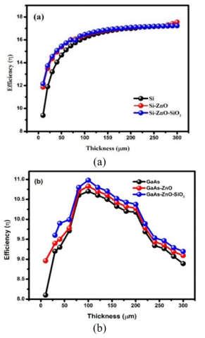
COMSOL multiphysics software was used for the effective analysis of the characteristics of the designed silicon solar cell. Each individual plot has its own uniqueness. In order to enhance the performance of the devices by compensating for the reflection from the top of the surface of the device, a bilayer antireflection coating consisting of silicon dioxide and zinc oxide was used as shown in Figure 2(b). In order to understand the impact of the existence of passive antireflective zinc oxide and silicon dioxide bulk layer on the performances of each type of solar cell, a number of simulations using the aforementioned software were performed. The schematic diagram of the devices is shown in Figures 1 and 2. The schematic diagram in Figure 1 represents cells without antireflection coating. The diagrams of Figure 2 represent structures of cells with zinc oxide and silicon dioxide anti-reflection coating. The area of the cells was 1cmx 1cm with a standardized thickness of 150µm for silicon and 80µm for gallium arsenide. The structures show the layer-wise deposition of two antireflection coatings. Materials with a band gap of 1.12eV for silicon, 1.424eV for gallium arsenide, 3.08eV for zinc oxide, and 9eV for silicon dioxide were used in simulation at a temperature of 293.15K. According to the requirement for high performance, the morphological structure consists of a high band gap to a low band gap from top to bottom. The characteristics of the cells were observed at a thickness of 0.5µm of zinc oxide and 0.5µm of silicon dioxide. Along with this, changes in parameters and device properties were studied by varying thickness from 10µm to 300µm of cell layers. The refractive index changes from 1.45 at top to 3.42 at bottom. Figure 3 shows the efficiency vs. thickness plot of silicon and gallium arsenide solar cells. The three different curves in Figure 3 represent the efficiency of the bare cell and the cell with antireflection coatings. Excitation coefficient, refractive index, absorption coefficient, etc. cannot be modified easily. So, the characteristic estimation was implemented by varying the thickness of the different layers of the cell. By using optimum thickness, devices show significant progress in their performance. For silicon solar cells, a rapid rise in efficiency from 9.4% to 16.75% i.e. approximately 2.65% in between 10µm to 150µm. Beyond that thickness rise in efficiency becomes unsubstantial. By varying thickness up to 300µm, there is a growth in efficiency. But the growth was obtained with the cost of bulkiness in the system and the growth rate was 0.005%. For gallium arsenide solar cells, a peak in efficiency is obtained at a cell thickness of 80µm. Beyond that thickness, efficiency scales down. Moving ahead along the rising scale of thickness, efficiency knocks off.
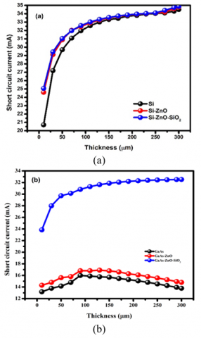
The results are advantageous with the indication that more charge carriers are due to the thicker device which enhance the efficiency. Another reason for enhancement may be the destructive interference which is due to the thickness of the layer and the refractive index. The results conferenced that the device performance not only changes due to the destructive interference but also changes due to surface recombination. Surface recombination is because of dangling bonds, which are generated due to defective structure. The research says more dangling bonds result in more surface recombination. With more defect, more dangling bonds reduces short circuit current in the case of gallium arsenide as shown in Figure 4, and enhances the efficiency. These dangling bonds can be reduced by doing thermal oxidation [4].
Figure 3. (a) Efficiency plot for silicon solar cell without and with antireflection coating (b) Efficiency plot for gallium arsenide solar cell without and with antireflection coating
Figure 4. (a) Short circuit current plot for silicon solar cell without and with antireflection coating (b) Short circuit current plot for gallium arsenide solar cell without and with antireflection coating
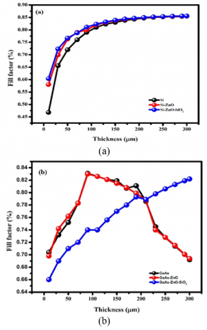
Figure 5. (a) Fill factor plot for silicon solar cell without and with antireflection coating (b) Fill factor plot for gallium arsenide solar cell without and with antireflection coating.
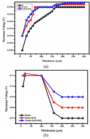
Figure 6. (a) Maximum voltage plot for silicon solar cell without and with antireflection coating (b) Maximum voltage plot for gallium arsenide solar cell without and with antireflection coating
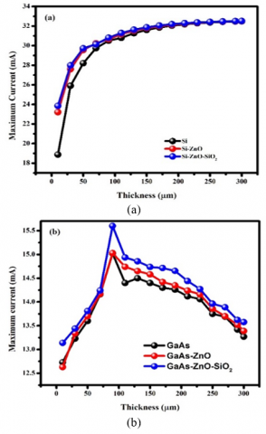
Figure 7. (a) Maximum current plot for silicon solar cell with antireflection coating (b) Maximum current plot for gallium arsenide solar cell with antireflection coating
Considering the design of the solar cells, electrical parameters have a more significant impact on the device. Impact of incident photon energy corresponding to wavelengths, short circuit current, open circuit voltage, fill factor, and calculation of optimum efficiency draws our overall attention. Figure 5 represents the different values of the fill factor with respect to the thickness of (a) Silicon solar cell and (b) Gallium arsenide solar cell. As the fill factors are associated with parasitic resistive losses, the structural part of the devices provides the effect of the fill factor on the performance due to the presence of series and shunt resistances. The observed results and the empirical formula both represent the fill factor as a function of normalized open circuit voltage with respect to the temperature. Simulated results say the optimum value of the fill factor for gallium arsenide with zinc oxide is 0.71. The designed devices were of less loss, so provides better efficiency. While considering this property, series resistance can be considered as a significant design parameter. Initially with less thickness, the fill factor curves approach to higher values, but with increased thickness, all the curves overlapped on each other. The three plots corresponding to a thickness of 200µm are getting closer to each other. Further with an increase in thickness, the fill factor curves merge following the same path. In fig-5(b), both the curves show 0.832 as the maximum value of the fill factor. Figure 5 represents an improvement in fill factor due to deposition of zinc oxide and silicon dioxide up to thickness of 200µm. Moving ahead to 200µm, the rate of improvement decreases, finally all three curves converge. This is due to a constant thickness of the anti-reflection coating layer and increasing thickness of emitter. Thicker emitter provides a dominant series resistance effect on thinner zinc oxide layer and silicon dioxide.
Proper function of the solar cells depends upon the amount of light incident on it. Light with different photon energy creates a challenge while designing a solar cell. So, our main objective is to inspect the device, at which point it will absorb maximum number of photons and refrains generated electron-hole pairs getting annihilated. Different measured values of the short circuit current shown in Figure 6, for (a) Silicon solar cell and (b) Gallium arsenide solar cell. All the curves in Figure 6(a) follow same pattern. It shows a significant rise in maximum voltage. As the thickness increases, number of charge carriers increases but not able to contribute towards generation. Due to which maximum voltage increases but remains constant afterwards. In case of gallium arsenide, it decreases as shown in Figure 6(b). The short circuit current also increases and then decreases due to the presence of zinc oxide and silicon dioxide layer, after that they moves along a single line as shown in Figure 7. Optimum current was observed at a thickness of 150µm for silicon solar cell, 80µm for gallium arsenide solar cell. If it is compared between all the two devices, latter device provides maximum short circuit current, maximum efficiency with higher thickness. The measured short circuit current was obtained from the standard 100mW/cm2 solar spectrum (AM 1.5). Absorbed photons and generated electron-hole pairs do not contribute towards the recombination.
The P-V and I-V characteristics of devices with antireflection coating were measured using COMSOL software under AM 1.5. The simulated values of the device parameters are summarized in Table 2.
Due to the use of zinc oxide and silicon dioxide antireflection coating, maximum power changes in order of 2% for silicon solar cell and 0.01% for gallium arsenide. No improvement in voltage due to higher thickness. This enhancement is because of maximum photo generated current. The enhancement in maximum current is due to suppressed reflection. This indicates antireflection layers plays an important role in suppressing the reflection.
Table 2. Electrical parameters of silicon and gallium arsenide solar cell
|
Sl No. |
Devices |
Efficiency (%) |
Short Circuit Current (mA/cm2) |
Fill Factor (%) |
Open Circuit Voltage (v) |
|
1 |
Si solar cell |
16.75% |
33.31 |
0.83 |
0.61 |
|
2 |
Si-ZnO solar cell |
16.85% |
33.5 |
0.84 |
0.61 |
|
3 |
Si-ZnO-SiO2 solarcell |
16.89% |
33.56 |
0.84 |
0.53 |
|
4 |
GaAs solar cell |
10.68% |
16 |
0.83 |
0.71 |
|
5 |
GaAs-ZnO solar cell |
10.69% |
16.02 |
0.83 |
0.71 |
|
6 |
GaAs-ZnO -SiO2 solar cell |
10.7% |
16.04 |
0.83 |
0.71 |
The present work evaluates the overall performance of the designed devices. The electrical properties of two designed devices with the presence of zinc oxide and silicon dioxide antireflection coating layer were investigated and analyzed. The analysis shows that the optimum performances are obtained at a thickness of 150µm for silicon and 80µm for gallium arsenide, beyond that there is an increase in efficiency and short circuit current, but the rate is quite less. It gives a clear picture that the deposition of zinc oxide and silicon dioxide anti-reflection coating layer enhances the properties of the device as expected. We obtained a simulated short circuit current density of 33.56mA/cm2, which is higher in comparison to the experimental obtained current density [13]. It is observed that with an increase in thickness, the short circuit current increases. Also, photo-generation rate gets affected by the change in thickness. This work provides a good idea of analysis and performance comparison by simulating the photovoltaic devices. Future work may comprise of different textures of the anti-reflection layer surfaces to enhance the efficiency.
[1] Missbach, T., Dengler, S.A., Siefer, G., Bett, A.W. (2018). High-speed quantum efficiency determination of multijunction solar cells. IEEE Journal of Photovoltaics, 8(1): 333-341. https://doi.org/ 10.1109/JPHOTOV.2017.2778043
[2] Sahoo, G.S., Mishra, G.P. (2019). Use of InGaAs/GaSb quantum ratchet in p-i-n GaAs solar cell for voltage preservation and higher conversion efficiency. IEEE Transactions on Electron Devices, 66(1): 153-159. https://doi.org/ 10.1109/TED.2018.2859766
[3] Shockley, W., Queisser, H.J. (1961). Detailed balance limit of efficiency of p-n junction solar cells. Journal of Applied Physics, 32: 510-519. https://doi.org/10.1063/1.1736034
[4] Sheng, X., Shen L., Kim T., et al. (2013). Doubling the power output of bifacial thin-film GaAs solar cells by embedding them in luminescent waveguides. Advanced Energy Materials, 3(8): 991-996. https://doi.org/10.1002/aenm.201201064
[5] Shahrjerdi, D., Bedell S.W., Bayram C., et al. (2013). Ultralight high-efficiency flexible InGaP/(In)GaAs tandem solar cells on plastic. Advanced Energy Materials, 3(5): 566-571.
[6] Miller, O.D., Yablonovitch, E., Kurtz, S.R. (2012). Strong internal and external luminescence as solar cells approach the Shockley-Queisser limit. IEEE Journal of Photovoltaics, 2(3): 303-311. https://doi.org/ 10.1109/JPHOTOV.2012.2198434
[7] Yeo, C.I., Kwon, J.H., Jang, S.J., Lee, Y.T. (2012). Antireflective disordered subwavelength structure on GaAs using spin-coated Ag ink mask. Optics Express, 20(17): 19554-19562. https://doi.org/10.1364/OE.20.019554
[8] Diedenhofen, S.L., Grzela, G., Haverkamp, E., Bauhuis, G., Schermer, J., Rivas, J.G. (2012). Broadband and omnidirectional anti-reflection layer for III/V multi-junction solar cells. Solar Energy Materials and Solar Cells, 101: 308-314. https://doi.org/10.1016/j.solmat.2012.02.022
[9] Yan, X., Poxson, D.J., Cho, J., Welser, R.E., Sood, A.K., Kim, J.K., Schubert, E.F. (2013). Enhanced omnidirectional photovoltaic performance of solar cells using multiple-discrete-layer tailored- and low-refractive index anti-reflection coatings. Advanced Functional Materials, 2013, 23(5): 583-590. https://doi.org/10.1002/adfm.201201032
[10] Zhao, J., Wang, A., Altermatt, P., Green, M. (1995). Twenty-four percent efficient silicon solar cells with double layer antireflection coatings and reduced resistance loss. Applied Physics Letters, 66(26): 3636-3638. https://doi.org/10.1063/1.114124
[11] Lee, S.E., Choi, S.W., Yi, J. (2000). Double-layer anti-reflection coating using MgF2 and CeO2 films on a crystalline silicon substrate. Thin Solid Films, 376(1-2): 208-213. https://doi.org/10.1016/S0040-6090(00)01205-0
[12] Doshi, P., Jellison, G.E., Rohatgi, A. (1997). Characterization and optimization of absorbing plasma-enhanced chemical vapor deposited antireflection coatings for silicon photovoltaics. Applied Optics, 36(30): 7826-7837. https://doi.org/10.1364/AO.36.007826
[13] Cid, M., Stem, N., Brunetti, C., Beloto, A., Ramos, C. (1998). Improvements in anti-reflection coatings for high-efficiency silicon solar cells. Surface and Coatings Technology, 106(2-3): 117-120. https://doi.org/10.1016/S0257-8972(98)00499-X
[14] Richards, B. (2003). Single-material TiO2 double-layer antireflection coatings. Solar Energy Materials and Solar Cells, 79(3): 369-390. https://doi.org/10.1016/S0927-0248(02)00473-7
[15] Hocine, D., Belkaid, M., Pasquinelli, M., Escoubas, L., Simon, J.J., Rivière, G.A., Moussi, A. (2013). Improved efficiency of multicrystalline silicon solar cells by TiO2 antireflection coatings derived by APCVD process. Materials Science in Semiconductor Processing, 16(1): 113-117. https://doi.org/10.1016/j.mssp.2012.06.004
[16] Swatowska, B., Stapinski, T., Drabczyk, K., Panek, P. (2011). The role of antireflective coatings in silicon solar cells—the influence on their electrical parameters. Optica Applicata, 41(2): 487-492.
[17] Gee, J.M., Gordon, R., Liang, H. (1996). Optimization of textured-dielectric coatings for crystalline-silicon solar cells. In 25th IEEE Photovoltaic Specialists Conference, pp. 733-736, Washington, DC, USA.
[18] Hashmi, G., Rashid, M.J., Mahmood, Z.H., Hoq, M., Rahman, M.H. (2018). Investigation of the impact of different ARC layers using PC1D simulation: Application to crystalline silicon solar cells. Journal of Theoretical and Applied Physics, 12: 327-334. https://doi.org/10.1007/s40094-018-0313-0
[19] Abdullah, H., Lennie, A., Ahmad, I. (2009). Modelling and simulation single layer anti-reflective coating of ZnO and ZnS for silicon solar cells using silvaco software. Journal of Applied Sciences, 9(6): 1180-1184. https://doi.org/10.3923/jas.2009.1180.1184
[20] Lennie A, Abdullah H, Shila Z, et al. (2010). Modelling and simulation of SiO2/Si3N4 as anti-reflecting. World Applied Sciences Journal, 11: 786-790.
[21] Wright, D., Marstein, E., Holt, A. (2005). Double layer anti-reflective coatings for silicon solar cells. In 31st IEEE Photovoltaic Specialists Conference, pp. 1237-1240. https://doi.org/10.1109/PVSC.2005.1488363
[22] Naser, N.M., Mustafa, B.T. (2017). Single layer anti-reflective (AR) coating silicon solar cells using simulation program. ZANCO Journal of Pure and Applied Sciences, 28(6): 39-43.
[23] Thosar, A.J., Thosar, M., Khanna, R. (2014). Optimization of anti-reflection coating for improving the performance of GaAs solar cell. Indian Journal of Science and Technology, 7(5): 637-641.
[24] Martínez, J.F., Steiner, M., Wiesenfarth, M., Glunz, S.W., Dimroth, F. (2019). Thermal analysis of passively cooled hybrid CPV module using Si cell as heat distributor. IEEE Journal of Photovoltaics, 9(1): 160-166. https://doi.org/10.1109/JPHOTOV.2018.2877004
[25] Solanki, C.S. (2012). Solar Photovoltaics: Fundamentals, Technology and Applications. PHI Learning Private Limited, New Delhi, India, Second edition, pp. 110-112.