Kheira Ouari*![]() | Kheira Ameur
| Kheira Ameur![]() | Halima Mazari
| Halima Mazari![]() | Abdelkader Nakrela
| Abdelkader Nakrela![]()
© 2024 The authors. This article is published by IIETA and is licensed under the CC BY 4.0 license (http://creativecommons.org/licenses/by/4.0/).
OPEN ACCESS
In the present paper, we have conducted both theoretical and experimental investigations on thin films of lead sulfide (PbS). The structural and morphological properties of these films, which were prepared using the spray pyrolysis method, were analyzed utilizing X-ray diffraction (XRD) and scanning electron microscopy (SEM). Theoretical calculations were performed employing the first principles full potential linearized augmented plane wave (FP-LAPW) approach. The findings of this study reveal that the PbS film that was deposited is polycrystalline and possesses a rock-salt structure. The SEM image depicts a planar structure with dimensions ranging from 480 to 930 nm. The results obtained through energy dispersive spectroscopy (EDS) indicate high crystalline quality, and the film surface exhibits a rough texture and a dense morphology. In terms of its behavior, PbS acts as a semiconductor with a direct optical band gap situated at the L point of the Brillouin zone (BZ). The density of states on both sides of the band gap is primarily of s-p character. The ionic nature of PbS can be attributed to charge transfer. A substantial level of agreement has been observed between the experimental and theoretical results. Our ongoing research endeavors aim to explore biosensors and their various applications. The novelty of this work lies in the combined study of the structural and morphological properties of PbS films grown using the spray pyrolysis technique, employing both experimental and theoretical approaches. This paper describes a comprehensive approach to understanding bulk and thin-film PbS materials through theory and experimentation.
FP-LAPW method, spray pyrolysis technique, EDS, lead sulfide
The investigation of innovative and functionalized materials has been of great importance for the progress and development of various technologies, such as those that depend on electrical [1], optical [2], and optoelectronic devices [3], as well as emerging technologies like quantum technologies [4]. These devices are expected to not only provide improved efficiencies but also facilitate the establishment of entirely new principles, which are highly desirable in modern information processing, quantum computing, medical technologies, and sensing applications. One such compound, lead sulfide (PbS), is particularly utilized in applications such as infrared radiation detectors, emitters, and solar control coatings [5]. PbS adopts the sodium chloride crystal structure [6] and possesses a direct band gap of 0.4 eV. Remarkably, its absorption coefficient progressively increases from the infrared to the visible region [7]. Furthermore, PbS exhibits a substantial exciton Bohr radius, estimated to be approximately 18 nm [8]. The ability to manipulate the energy band gap through the modification of particle size in nanostructures allows for the control of this semiconductor material [9]. Consequently, PbS finds utility in various fields, including radiation absorption [10], selective Pb2+ sensors [11], and photography [12]. In recent times, PbS has been employed in diverse applications such as temperature sensors, humidity sensors, photoresistors, solar control coatings, decorative coatings, diode lasers, and biosensors [13-15]. For instance, Liu et al. [16] investigated the utilization of lead sulfide in a gas sensor for the detection of H2S gas, aiming to develop a low-cost and high-performance sensor based on PbS. Similarly, Mosahebfard et al. [17] explored the fabrication of a methane gas sensor with enhanced sensor characteristics, such as response, sensitivity, speed, and linearity, using lead sulfide at room temperature.
The design and fabrication of optoelectronic devices based on PbS necessitate a thorough understanding of the material's optical properties and electronic structure. In this regard, Nanda et al. [18] focused on the band gap tuning of PbS nanoparticles through the in-flight sintering of size-classified aerosols. Their investigation resulted in a band gap range of 0.5-2.0 eV, revealing that the band gap initially decreases and then increases with increasing sintering temperature. The nature of the substrate and crystal growth conditions significantly influence the attainment of these properties. Several researchers have employed various deposition techniques to study PbS, with microwave heating [19, 20], electro-deposition [21, 22], chemical bath deposition [23-25], and spray pyrolysis [26] being the most commonly utilized methods. Notably, this work stands out due to its comprehensive investigation of the structural and morphological properties of PbS films grown using the spray pyrolysis technique, employing both experimental and theoretical approaches. Hence, this paper presents a comprehensive methodology for understanding bulk and thin-film PbS materials through a combination of theory and experimentation.
PbS thin films were produced on glass substrates through the utilization of the spray pyrolysis method. The configuration utilized in the experiment closely mirrored that specified in study [27]. The glass substrates underwent a thorough purification process, which entailed being treated with freshly prepared chromic acid, a solution of detergent, and distilled water. The spray solution, comprising of 0.05 M PbCl2H2O and 0.05 M CH4N2S, was dissolved in bidistilled water. A carrier gas of compressed air at a pressure of 6 N/cm2 was employed, along with a solution flow rate of 5 cm3/min. The temperature of the substrate was sustained at 300℃ and controlled via a thermocouple (Chrome-Nickel). Standard quality glass slides, originally sourced from China (Glass Slide Microscopic REF 217102), were utilized for the analysis. These slides were precisely cut into square fragments measuring approximately 2.5 cm × 2.5 cm × 1 mm for the application of the thin films. Before commencing the deposition process, the slides underwent cleaning procedures that involved washing with a mixture of water and detergent powder, as well as a 10-minute ultrasonic cleaning session. Subsequently, they were rinsed in distilled water and subjected to an additional 10-minute ultrasonic cleaning treatment before being dried. Following these steps, the slides were immersed in 99.99% purity ethanol for a 10-minute ultrasonic cleaning technique, and then dried using hot air and specialized drying paper, making them suitable for integration into the spray pyrolysis system. The structural analysis was carried out at room temperature in the θ-2θ scan mode utilizing a Rigaku Miniflex diffractometer (CuKα radiation, λ = 1.5406 Å). Scanning electron microscopy (SEM) was employed to examine the surface morphology of the PbS thin films.
The theoretical calculations were conducted utilizing the full potential linearized augmented plane wave (FP-LAPW) method [28] founded on the density-functional theory (DFT) [29]. The Perdew-Zunger scheme [30], as implemented in the WIEN 97 code [31], was employed to describe the exchange-correlation energy of the electrons in the local-density approximation (LDA). In order to extend the basis functions, a hybrid approach was employed, combining spherical harmonic functions in non-overlapping spheres encompassing the atomic sites (referred to as muffin-tin spheres) and Fourier series in the interstitial region. Within the muffin-tin spheres (MTS), an L-expansion of the non-spherical potential and charge density was conducted up to LMAX = 10, requiring the utilization of 470 plane waves for expanding the charge density and potential in the interstitial region. The energy cutoff was established at RMT KMAX = 7, where KMAX denotes the maximum modulus for the reciprocal lattice vector and RMT represents the radius of the MTS. Furthermore, specific values of 2.5 atomic units for Pb and 2.2 atomic units for S were chosen to ensure a precise treatment of core and valence electrons within the muffin-tin spheres, while simultaneously upholding computational efficiency [32].
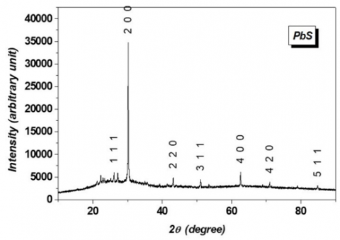
The structural analysis was conducted at ambient temperature utilizing a Rigaku Miniflex X-ray diffractometer with Cukα radiation having a wavelength of 1.5406 Å. Figure 1 exhibits the XRD patterns of our deposited PbS thin film.
Figure 1. X-ray diffraction patterns of PbS thin film
It is evident that the diffracted peaks positioned at 2θ = 26.034º, 30.141º, 43.057º, and 50.97º correspond to the crystallographic planes of the Miller indices (111), (200), (220), and (311), respectively, which are in concordance with the 78-1897 JCPDS X-ray powder data file. The deposited film possesses a rock salt structure. Comparable findings were documented in the scientific literature [33]. The lattice constant a is determined through the utilization of the subsequent equation.
$d_{(h k l)}=\frac{a}{\sqrt{h^2+k^2+l^2}}$ (1)
where, h, k, l represent the Miller's crystallographic indices. The lattice constant of the final product, as determined from the XRD pattern, was a = 5.933 Å, in good agreement with the value of 5.936 Å reported in Joint Committee on Powder Diffraction Standards (JCPDS) ICDD1993 card no. 5-592. This value is close to the lattice parameter reported for PbS (a = 5.936 Å) [32].
The average grain size (D) of PbS films was evaluated through the peak full width at half maximum (FWHM) of a peak (B), implementing the Scherrer formula [34]:
$D=\frac{0.9 \lambda}{B \cos \theta}$ (2)
where, λ denotes the wavelength of X-ray radiation, θ signifies the Bragg angle of the peaks, and B denotes the angular width of peaks at FWHM. The calculated average grain size of the PbS film was found to be 502 Å. The values of the lattice constant a (5.926 Å) and the average grain size align satisfactorily with prior outcomes [35].
Bortamuly et al. [33] applied the chemical technique of Bath Deposition (CBD), inferring a crystallite size of approximately 247 Å. Rajathi et al. [35] estimated the lattice parameter value for PbS thin film to be approximately 5.936 Å and the average crystallite size to be 740 Å (utilizing the Debye-Scherrer formula) [34]. It is well known that the distinctive growth, size, and shape of the grains, which directly impact the characteristics and properties of the films, are connected with each deposition mechanism [36]. Thus, the spray pyrolysis technique represents a straightforward and cost-effective approach for the fabrication of thin films.
When considering the analysis of grain sizes utilizing the Scherrer formula, the focus was on the importance of particle dimensions in nanostructured materials. The determination of the average size of coherent scattering regions through the Scherrer formula and X-ray powder diffraction methods is of significant importance [37]. It is noteworthy that despite efforts to improve the formula's precision, uncertainties persist regarding its practical range of application. Furthermore, elucidating the theoretical upper limit of the formula, it has been disclosed that it can be employed up to 600 nm for specific substances [38], demonstrating enhanced accuracy for particle sizes below 60 nm [39].
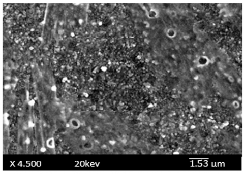
Figure 2. PbS thin film SEM micrograph
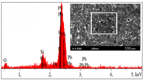
Figure 2 illustrates a micrograph taken by a scanning electron microscope (SEM) which exhibits the intensive and rough morphology of the PbS film. The surface presents a dense appearance, entirely covered by PbS nanoparticles, and devoid of any discernible cracks when examined over a significant scanning area. In Figure 3, the Energy Dispersive Spectroscopy (EDS) analysis provides an accurate determination of the composition, revealing the presence of Pb, S, and O within the thin film.
Figure 3. EDS spectrum of the PbS thin film (the figure inside shows the exact position of the treated microstructure)
The identification of Si is attributed to the influences of the substrate. The EDS data presented herein corroborates the findings obtained from the X-ray diffraction (XRD) analysis.
Further elaboration on the chemical composition, including the percentage of element concentrations in the PbS thin film, is succinctly summarized in Table 1.
Table 1. Element concentrations in PbS thin film
|
Elements |
Pb |
S |
Si |
|
Concentrations at % |
31.64 |
38.71 |
29.65 |
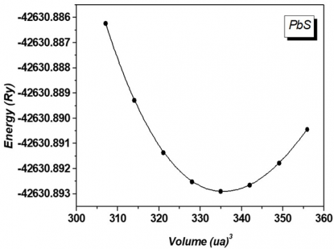
For the sake of specificity, we have also conducted a theoretical calculation of the structural characteristics of our compound. The total energies have been computed based on a specified array of lattice constants. Our data originates from the optimal agreement achieved through the utilization of the Murnaghan equation of state [40].
Hence, in order to ascertain the equilibrium parameters such as the lattice constant a, the total energy was assessed in relation to the volume, and the resultant plot was adjusted utilizing the Murnaghan equation as follows:
$E(V)=E_0+\frac{B_0}{B'(B'-1)}\left[V\left(\frac{V_0}{V}\right)^{B^{\prime}}-V_0\right]+\frac{B_0}{B'}\left(V-V_0\right)$ (3)
where, E0, V0, B and B' are respectively: the total energy, the equilibrium volume, the bulk modulus, and its derivative. One must highlight that the utility of this equation diminishes as compression ratios surpass around 0.7-0.8 times the original volume [41], owing to the direct correlation between pressure, bulk modulus, and the pressure derivative of the bulk modulus.
Figure 4 shows the total energy as a function of the volume for PbS.
Figure 4. Calculated total energy as a function of volume of PbS
The obtained lattice parameter a, which is measured to be 5.842 Å, exhibits a decrease in comparison to the experimental value as a consequence of limitations inherent to the LDA calculations.
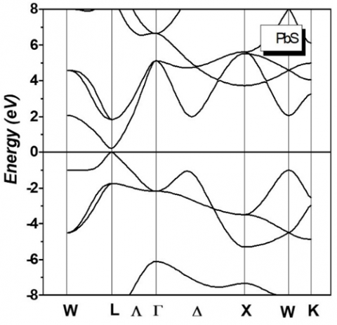
The band structure describes the relationship between the energy of a particle and its wave vector E(k). The band structure of PbS, as shown in Figure 5, is derived using the FP-LAPW approach. A band gap of 0.2 eV is calculated through the LDA-based FLAPW method. The valence band maximum and conduction band minimum are both situated at the L point, indicating a direct gap.
Figure 5. Band structure for PbS
Table 2 presents a comparison between the empirical measurements of the lattice constant and the bandgap and the theoretical values derived through the utilization of the LDA-based FLAPW technique.
Table 2. Element concentrations in PbS thin film
|
Material |
Theoretical Value (Our Results) |
Experimental Value (Our Results) |
||
|
PbS |
Lattice constant (Å) |
Bandgap (eV) |
Lattice constant (Å) |
Bandgap (eV) |
|
5.842 |
0.2 |
5.926 |
/ |
|
According to the data provided in this table, the observed value of the lattice constant a aligns well with both the theoretically derived value from our calculations and the value obtained from existing literature [38].
In relation to the bandgap (Theoretical value), Jahromi and Moaddeli [42] utilized the Perdew-Burke-Ernzerhof (PBE) functional approach across the Brillouin zone in their investigation. Within their study, they reported a value of Eg = 0.27 eV for PbS which is in concurrence with the value of 0.2 eV obtained by employing the FP-LAPW method in our computational analysis. Nevertheless, this theoretical value is lower than the experimental value of 0.41 eV determined by previous studies [43, 44]. This discrepancy is likely attributed to the LDA based FLAPW approximation, which tends to underestimate gaps for compound semiconductors, as indicated by the research conducted by Lew Yan Voon et al. [45].
The Full-Potential Linearized Augmented Plane Wave (FPLAPW) technique stands out as one of the most precise approaches for computing electronic structures, especially in the case of materials possessing intricate crystal configurations [46]. Nevertheless, it has been extensively documented that within semiconductors, despite the utilization of FPLAPW, the Local Density Approximation (LDA) consistently underpredicts band gaps, resulting in notable discrepancies.
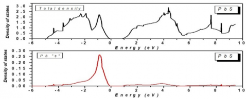
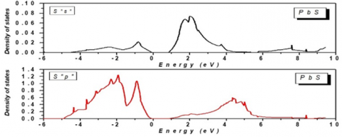
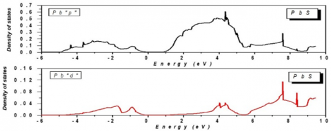
The integrated densities of states, both total and partial, for the DOS and PDOS, are displayed in Figure 6, encompassing the atoms as well as the interstitial area outside the MTS. By means of the latter, one can acquire a comprehension of the overall bonding characteristics present in this compound. The total density of states showcases two distinctive regions: (i) the bands spanning from -5 eV to the valence band maximum are principally derived from the S3p-states, with only a minor inclusion of Pb6S and 6p-states; (ii) the states within the conduction band solely consist of Pb-p states, which are then intertwined with S-p states.
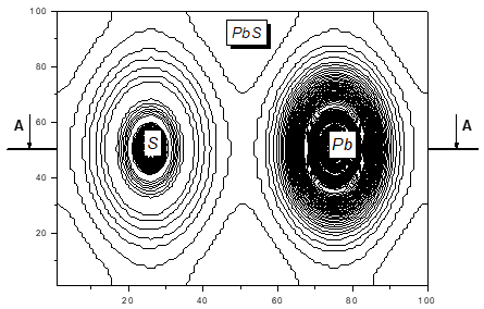
The total density of charge in the valence band is represented along the PbS bonds and within the (110) plane that encompasses the Pb and S atoms, as shown in Figure 7. The transfer of charge is responsible for the ionic nature of PbS. The primary factor driving the displacement of bonding charge is the heightened electron-attracting ability of sulfur due to the difference in electronegativity between sulfur and lead.
Figure 7. Contour plot of the total valence charge density in the (110) plane of PbS
In summary, our study presents an inquiry into the structural, morphological, and theoretical characteristics of lead sulfide. By utilizing the spray pyrolysis technique, we successfully fabricated PbS films and subsequently examined them using X-ray diffraction (XRD) and scanning electron microscopy (SEM). Theoretical calculations were conducted employing the FP-LAPW method. Our findings indicate that the deposited PbS film exhibits a polycrystalline structure resembling that of rock salt, thereby demonstrating a strong concurrence between the calculated and experimental lattice constants. Scanning electron microscopy (SEM) presents an image of a flat structure with measurements ranging from 480 to 930 nm, consistent with Scherrer Debye calculations. The results from energy-dispersive X-ray spectroscopy (EDS) confirm the high quality of crystallinity, while the surface of the film displays an overall roughness and dense morphology. Identified as a semiconductor, PbS possesses a direct optical band gap of approximately 0.41 eV, situated at the L point of the Brillouin Zone (BZ). However, our study indicates that the actual band gap is around 0.2 eV. The density of states on both sides of the gap demonstrates an s-p character, and the calculated distribution of electron charge suggests an ionic nature.
Furthermore, due to its compelling characteristics related to its band gap, PbS has emerged as a preferred material for a variety of applications in the realm of optics (such as semiconductor nanoparticle-based lasers), photovoltaics (utilizing solar cells capable of absorbing far infrared radiation), photodetection (providing highly sensitive photodetectors), and telecommunications. Our current research focuses on the utilization of biosensors, with a particular emphasis on the exceptional potential of PbS nanoparticles for developing glucose sensors. Recent studies have shown that glucose sensors incorporating PbS nanoparticles demonstrate notably enhanced sensitivity in comparison to sensors utilizing alternative semiconductor materials. Therefore, there is a strong rationale to posit that PbS-based glucose sensors could outperform those based on other available materials. This comprehensive investigation on PbS was conducted to explore this possibility.
Looking forward, it is crucial to utilize alternative approximations such as GGA-PBEsol (generalized gradient approximation Perdew-Burke-Ernzerhof) in order to facilitate a comparison with the results obtained from the LDA-based FLAPW approximation.
The authors thank the research laboratory LECM of the University Djillali Liabes of Sidi Bel Abbes for their technical support during the experimental work.
[1] Akinwande, D., Petrone, N., Hone, J. (2014). Two-dimensional flexible nanoelectronics. Nature Communications, 5(1): 5678. https://doi.org/10.1038/ncomms6678
[2] Che, Y., Chen, H., Gui, H., Liu, J., Liu, B., Zhou, C. (2014). Review of carbon nanotube nanoelectronics and microelectronics. Semiconductor Science and Technology, 29(7): 073001. https://doi.org/10.1088/0268-1242/29/7/073001
[3] Brosseau, C. (2011). Emerging technologies of plastic carbon nanoelectronics: A review. Surface and Coatings Technology, 206(4): 753-758. https://doi.org/10.1016/j.surfcoat.2011.02.017
[4] Noda, S. (2006). Seeking the ultimate nanolaser. Science, 314(5797): 260-261. https://doi.org/10.1126/science.1131322
[5] Onwudiwe, D.C. (2019). Microwave-assisted synthesis of PbS nanostructures. Heliyon Journal, 5(3): e01413. https://doi.org/10.1016/j.heliyon.2019.e01413
[6] Davar, F., Mohammadikish, M., Loghman-Estarki, M. R., Masteri-Farahani, M. (2014). Synthesis of micro-and nanosized PbS with different morphologies by the hy-drothermal process. Ceramics International, 40(6): 8143- 8148. https://doi.org/10.1016/j.ceramint.2014.01.009
[7] Johnson, T.H. (1983). Lead salt detectors and arrays PbS and PbSe. In 27th Annual Technical Symposium (SPIE 0443) Infrared Detectors, San Diego, United States, 443: 60-94. https://doi.org/10.1117/12.937940
[8] Madelung, O. (2004). Semiconductors: Data Handbook, 3rd ed. Springer, Berlin. https://doi.org/10.1007/978-3-642-18865-7
[9] Rafea, M.A., Roushdy, N. (2010). Study of optical properties of nanostructured PbS Films. Philosophical Magazine Letters, 90(2): 113-120. https://doi.org/10.1080/09500830903459663
[10] Nair, P.K., Gomezdaza, O., Nair, M.T.S. (1992). Metal sulphide thin film photography with lead sulphide thin films. Advanced Materials for Optics and Electronics, 1(3): 139-145. https://doi.org/10.1002/amo.860010307
[11] Hirata, H., Higashiyama, K. (1971). Analytical study of the lead ion-selective ceramic membrane electrode. Bulletin of the Chemical Society of Japan, 44(9): 2420-2423. https://doi.org/10.1246/bcsj.44.2420
[12] Seghaier, S., Kamoun, N., Brini, R., Amara, A.B. (2006). Structural and optical properties of PbS thin films deposited by chemical bath deposition. Materials Chemistry and Physics, 97(1): 71-80. https://doi.org/10.1016/j.matchemphys.2005.07.061
[13] Nair, P.K., Garcia, V.M., Hernandez, A.B., Nair, M.T. S. (1991). Photoaccelerated chemical deposition of PbS thin films: Novel applications in decorative coatings and imaging techniques. Journal of Physics D: Applied Physics, 24(8): 1466-1472. https://doi.org/10.1088/0022-3727/24/8/036
[14] Ileana, P., Nascu, C., Ionescu, V., Indrea, E., Bratu, I. (1997). Structural and optical properties of PbS thin films obtained by chemical deposition. Thin Solid Films, 307(1-2): 240-244. https://doi.org/10.1016/s0040-6090(97)00304-0
[15] Zhao, Y., Huang, J., Huang, Q., Tao, Y., Gu, R., Li, H.Y., Liu. H. (2022). Electrochemical biosensor employing PbS colloidal quantum dots/Au nanospheres-modified electrode for ultrasensitive glucose detection. Nano Research, 16(3): 4085-4092. https://doi.org/10.1007/s12274-022-5138-0
[16] Liu, H., Li, M., Shao, G., Zhang, W., Wang, W., Song, H., Cao, H., Ma, W., Tang, J. (2015). Enhancement of hydrogen sulfide gas sensing of PbS colloidal quantum dots by remote doping through ligand exchange. Sensors & Actuators, B: Chemical, 212: 434-439. https://doi.org/10.1016/j.snb.2015.02.047
[17] Mosahebfard, A., Jahromi, H.D., Sheikhi, M.H. (2016). Highly sensitive, room temperature methane gas sensor based on lead sulfide colloidal nanocrystals. IEEE Sensors Journal, 16(11): 4174-4179.
[18] Nanda, K.K., Kruis, F.E., Fissan, H., Acet, M. (2022). Band-gap tuning of PbS nanoparticles by in -flight sintering of size classified aerosols. Journal of Applied Physics, 91(4): 2315-2321. https://doi.org/10.1063/1.1431429
[19] Slonopas, A., Alijabbari, N., Saltonstall, C., Globus, T., Norris, P. (2015). Chemically deposited nanocrytalline lead sulfide thin films with tunable properties for use photovoltaics. Electrochimica Acta, 151(1): 140-149. https://doi.org/10.1016/j.electacta.2014.11.021
[20] Thangaraju, B., Kalainnan, P. (2000). Spray pyrolytically deposited PbS thin films. Semiconductor Science and Technology, 15(8): 849-853. https://doi.org/10.1088/0268-1242/15/8/311
[21] Ni, Y., Wang, F., Liu, H., Yin, G., Hong, J., Ma, X., Xu, Z. (2004). A novel aqueous-phase route to prepare flower-shaped PbS micron crystals. Journal of Crystal Growth, 262(1-4): 399-402. https://doi.org/10.1016/j.jcrysgro.2003.10.053
[22] Zhao, Y., Liao, X.H., Hong, J.M., Zhu, J.J. (2004). Synthesis of lead sulfide nanocrystals via microwave and sonochemical methods. Materials Chemistry and Physics, 87(1): 149-153. https://doi.org/10.1016/j.matchemphys.2004.05.026
[23] Nascu, C., Vomir, V., Pop, I., Ionescu, V., Grecu, R. (1996). The study of lead sulphide films. VI. Influence of oxidants on the chemically deposited PbS thin films. Materials Science and Engineering: B, 41(2): 235-240. https://doi.org/10.1016/s0921-5107(96)01611-x
[24] Larramendi, E.M., Calzadilla, O., Gonzalez-Arias, A., Hernandez, E., Ruiz-Garcia, J. (2001). Effect of surface structure on photosensitivity in chemically deposited PbS thin films. Thin Solid Films, 389(1-2): 301-306. https://doi.org/10.1016/s0040-6090(01)00815-x
[25] Pentia, E., Pintilie, L., Tivarus, C., Pintile, I., Botila, T. (2001). Influence of Sb3+ ions on photoconductive properties of chemically deposited PbS films. Materials Science and Engineering: B. 80(1-3): 23-26. https://doi.org/10.1016/s0921-5107(00)00578-x
[26] Joshi, R.K., Kanjilal, A., Sehgal, K.H. (2004). Solution grown PbS nanoparticle films. Applied Surface Science, 221(1-4): 43-47. https://doi.org/10.1016/s0169-4332(03)00955-3
[27] Faraj, M.G. (2015). Effect of thickness on the structural and electrical properties of Spray pyrolysed lead sulfide thin films. American Journal of Condensed Matter Physics, 5(2): 51-55. https://doi.org/10.56431/p-9q31z4
[28] Jansen, H.J.F., Freeman, A.J. (1984). Total-energy full potential linearized augmented-plane-wave method for bulk solids: Electronic and structural properties of tungsten. Physical Review B, 30(2): 561-569. https://doi.org/10.1103/physrevb.30.561
[29] Hohenberg, P., Kohn, W. (1964). Inhomogeneous electron gas. Physical Review B, 136(3B): 864-871. https://doi.org/10.1103/physrev.136.b864
[30] Perdew, J.P., Wan, Y. (1992). Accurate and simple analytic representation of the electron-gas correlation energy. Physical Review B, 45(23): 13244-13249. https://doi.org/10.1103/physrevb.45.13244
[31] Blaha, P., Schwarz, K., Luitz, J. (1997). WIEN 97, Vienna University of Technology (Improved and updated UNIX version of the original copyrighted WIEN-code).
[32] Rajashree, C., Balu, A.R., Nagarethinam, V.S. (2015). Properties of Cd doped PbS thin films: Doping concentration effect. Surface Engineering, 31(4): 319–321. https://doi.org/10.1179/1743294415y.0000000014
[33] Bortamuly, G., Chetri, P., Bardaloi, S. (2021). Effect of lead (Pb) concentrations on structural & optical properties of PbS thin films. Indian Journal of Pure & Applied Physics, 59(06): 447-451. https://doi.org/10.56042/ijpap.v59i6.41650
[34] Rubin, K.A., Chen, M. (1989). Progress and issues of phase-change erasable optical recording media. Thin Solid Films, 181(1-2): 129-139. https://doi.org/10.1016/0040-6090(89)90479-3
[35] Rajathi, S., Kirubavathi, K., Selvaraju, K. (2017). Structural, morphological, optical, and photoluminescence properties of nanocrystalline PbS thin films grown by chemical bath deposition. Arabian Journal of Chemistry, 10(8): 1167-1174. https://doi.org/10.1016/j.arabjc.2014.11.057
[36] Farshidi, H., Rashidi, A., Youzbashi, A.A., Saani, M.H. (2019). Morphology control of chemically deposited nanostructured PbS thin films. Journal of Interfaces, Thin Films, and Low Dimensional Systems, 3(1): 245-250. https://doi.org/10.22051/jitl.2020.25675.1028
[37] Ingham, B. (2015). X-ray scattering characterisation of nanoparticles. Crystallography Reviews, 21(4): 229-303. https://doi.org/10.1080/0889311x.2015.1024114
[38] Muniz F.T.L., Miranda M.A.R., dos Santos C.M., Sasaki J.M. (2016). The Scherrer equation and the dynamical theory of X-ray diffraction. Acta Crystallographica A: Foundations and Advances, 72(3): 385-390. https://doi.org/10.1107/s205327331600365x
[39] Miranda M.A.R., Sasaki J.M. (2018). The limit of application of the Scherrer equation. Acta Crystallographica A: Foundations and Advances, 74(1): 54-65. https://doi.org/10.56042/ijpap.v59i6.41650
[40] Murnaghan, F.D. (1944). The compressibility of media under extreme pressures. Proceedings of the National Academy of Sciences, 30(9): 244-247. https://doi.org/10.1073/pnas.30.9.244
[41] Anderson, O.L. (1995). Equations of State of Solids for Geophysics and Ceramic Science. Oxford University Press. https://doi.org/10.1093/oso/9780195056068.001.0001
[42] Jahromi, H.D., Moaddeli, M. (2019). Lead sulfide; A new candidate for optoelectronics applications in the ultra violet spectral range. Materials Research Express, 6(11): 116220. https://doi.org/10.1088/2053-1591/ab513d
[43] Fatemi, A., Tohidi, T., Jamshidi Galeh, K., Rasouli, M., Ostrikov, K. (2022). Optical and structural properties of Sn and Ag-doped PbS/PVA nanocomposites synthesized by chemical bath deposition. Scientific Reports, 12(12893): 1-12. https://doi.org/10.1038/s41598-022-16666-6
[44] Lin, P.J., Kleinman, L. (1966). Energy bands of PbTe, PbSe and PbS. Physical Review, 142(2): 478-489. https://doi.org/10.1103/physrev.142.478
[45] Lew Yan Voon, L.C., Willatzen, M., Cardona, M. (1996). Terms linear in k in the band structure of wurtzite-type semiconductors. Physical Review B, 53(16): 10703-10714. https://doi.org/10.1103/physrevb.53.10703
[46] Alay-e-Abbas, S.M., Shaukat, A. (2011). FP-LAPW calculations of structural, electronic, and optical properties of alkali metal tellurides: M2Te [M: Li, Na, K and Rb]. Journal of Materials Science, 46: 1027-1037. https://doi.org/10.1007/s10853-010-4868-7