
Mohammad Tariq Yaseen* | Ahmad A. Ismael | Shamil H. Hussein | Ahmed S. Al-Jawadi
© 2026 The authors. This article is published by IIETA and is licensed under the CC BY 4.0 license (http://creativecommons.org/licenses/by/4.0/).
OPEN ACCESS
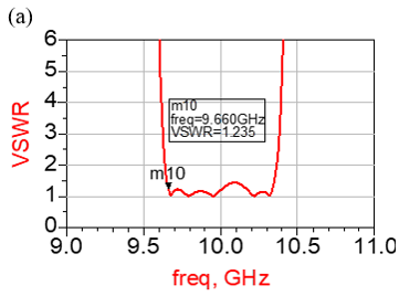
In this paper, a fifth-order X-band parallel-coupled microstrip bandpass filter has been designed for high frequency resonator applications. In order to compensate the frequency detuning caused by the open-ended coupled lines fringing capacitance, Reverse Dielectric Calibrating approach has been implemented. By reversing the dielectric constant calculation from 3.78 to 3.39, the effective dielectric constant has been increased, thus the additional electrical length has been compensated and the desired resonant frequency has been retrieved. The designed filter has been modeled and optimized by using the Advanced Design System (ADS) software at the central frequency of 10 GHz. The simulated results indicate that the proposed filter has passband bandwidth of 800 MHz, which corresponds to 8% of the fractional bandwidth. The simulated insertion loss is about −0.144 dB, while the return loss is about −14.95 dB at the resonant frequency of 9.660 GHz. The calculated voltage standing wave ratio at 9.660 GHz is equal to 1.235, and it remains below 1.5 within the filter passband, thus good impedance matching has been achieved. The introduced approach enables frequency correction and adequate passband characteristics of X-band microstrip filters.
microstrip bandpass filter, X-band, parallel coupled line, parasitic compensation, multi-harmonic response, convolutional neural networks
In recent years, wireless communication systems, particularly those operating within the X-band frequency range (such as radar systems and satellite communications), have seen an increasing demand for high-precision and compact components. Bandpass filters (BPF) based on parallel coupled microstrip line technology are among the most critical components due to their ease of fabrication and seamless integration with Microwave Integrated Circuits (MICs) [1-3].
For X-band (around 10 GHz) parallel coupled microstrip bandpass filters are highly sensitive to parasitic effects. The fringing fields at the ends of the coupled resonators lead to additional parasitic capacitance, which increases the effective length of the lines and thus deviates the center frequency of the filter from the design value. While there are also publications on new types of filters as well as realizations in different technologies, the majority of the papers do not deal with the problem of the parasitic capacitance in the classical parallel coupled microstrip resonators directly [4]. Compensation of the caused detuning of the filter is of major interest in order to increase selectivity, bandwidth, compactness as well as suppression of harmonic frequencies. For 10 GHz bandpass filters even smallest changes of the effective permittivity, the line distance as well as the electrical length of the resonators have a great impact on the pass band characteristics of the filter. In this contribution a Reverse Dielectric Calibrating approach is presented and for verification by means of simulations is applied in order to compensate the detuning caused by the parasitic capacitance and to achieve the desired X-band characteristics [5].
Liang and Chen [6] offered a filtering patch antenna using parasitic patches giving good performance for X-band filtering applications. It achieved good results that comply with engineering standards, as the filter operates at a center frequency of 10 GHz with a minimal error margin and a bandwidth of 800 MHz. The gain of the filter was close to the ideal value, ensuring high-efficiency energy transfer within the passband. The matching was ideal with the filter input, where the S-parameter (S11) values reached -15 dB at their lowest level, which effectively contributes to reducing the reflected power. The validity of the filter design at the fifth order was verified through impedance analysis with the presence of five distinct resonant poles.
2.1 Design specifications
The design process began by defining the basic parameters required for the filter, which are as follows: Filter type: Bandpass filter with parallel coupled microstrip lines. Center frequency at 10 GHz. Sub bandwidth (Delta): 10% (i.e., 1 GHz). Response type: Chebyshev waveform of 0.5 dB. Filter order: n = 5 (resulting in 6 coupling stages). Dielectric constant (εr): 3.78. Dielectric thickness (H): 15 mils. Copper conductor thickness (T): 1.4 mil.
2.2 Admittance inverter constants for the bandpass filter design
To convert the typical Chebyshev response (Low-pass prototype) into a Bandpass design, we use the J parameters. These parameters are calculated using the typical values g0, g1, ..., gn according to the following equations [7-10]:
For the first stage:
$Z_0 J_{01}=\sqrt{\frac{\pi \Delta}{2 g_0 g_1}}$ (1)
For intermediate stages (j = 1 to n-1):
$Z_0 J_{j, j+1}=\frac{\pi \Delta}{2 \sqrt{g_j g_{j+1}}}$ (2)
For the final stage:
$Z_0 J_{n, n+1}=\frac{\pi \Delta}{2 \sqrt{g_n g_{n+1}}}$ (3)
Calculating even and odd mode impedances once the JZ0 values are obtained for each stage, the even (Zoe) and odd (Zoo) mode impedances are extracted using the following equations, as shown in Table 1, where Z0 = 50 Ω.
$Z_{o e}=Z_o\left[1+J Z_o+\left(J Z_o\right)^2\right]$ (4)
$Z_{o o}=Z_o\left[1-J Z_o+\left(J Z_o\right)^2\right]$ (5)
Table 1. Calculated even and odd mode impedances
|
Section |
JZ0 |
Zoe (Ω) |
Zoo (Ω) |
|
Section 1 & 6 |
0.261 |
66.5 |
40.3 |
|
Section 2 & 5 |
0.064 |
53.3 |
47.0 |
|
Section 3 & 4 |
0.048 |
52.5 |
47.7 |
The next step relies entirely on the values obtained in the previous steps; it involves converting the electric field to the physical field, which yields the dimensions W, S, and L. This is done using the DS LineCalc tool.
2.3 Physical dimensions of microstrip lines
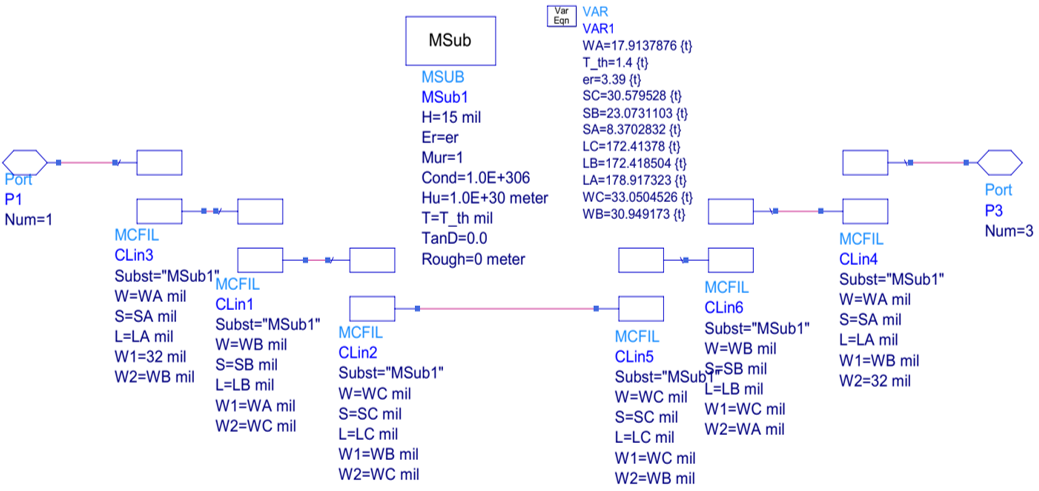
Here we describe the process of how the lines were calculated for the microstrip filter [11]. For the synthesis of the coupled lines the odd and even mode impedances were transformed to line width, line spacing and physical length [12]. These values were used to synthesize the lines for the filter to work at 10 GHz using the LineCalc tool in the Advanced Design System (ADS), as shown in Figure 1, and the resulting initial values for the filter are listed in Table 2.
Figure 1. Microstrip parallel coupled line filter
Table 2. Transmission line sections parameters
|
Section |
Width W (mil) |
Spacing S (mil) |
Length L (mil) |
|
Stage 1 & 6 |
25.46 |
6.97 |
177.8 |
|
Stage 2 & 5 |
29.95 |
33.41 |
173.4 |
|
Stage 3 & 4 |
30.04 |
42.58 |
173.4 |
Due to the high frequency, the open ends of the resonators cause fringing fields and thus additional parasitic capacitance. The electrical length of the coupled line sections is increased by these fringing fields and must be compensated in the design. In the initial simulation, the center frequency of 9.5 GHz was obtained with the nominal value of the relative permittivity of the substrate, εr = 3.78. To compensate for this frequency deviation a Reverse Dielectric Calibrating, called calibration for short, is applied in ADS by using an equivalent value of εr = 3.39 for the design. This value must not be confused with the dielectric constant of the actually used substrate. The value of εr = 3.39 is used as a design parameter in order to achieve the required effective electromagnetic behavior. The compensation of the additional electrical length can be performed by physical compensation, i.e., by retuning the coupled-line width, the line spacing, the resonator length and the open-end correction.
The Reverse Dielectric Calibrating approach is used to determine an equivalent design parameter, the dielectric constant of the substrate. This dielectric constant is a fixed property of the actual substrate used for the microstrip structures. Thus, the equivalent dielectric constant obtained from the Reverse Dielectric Calibrating approach is translated into the physical microstrip dimensions, for instance the line width, the line spacing, the length of the resonators, and the open-end corrections, which all together reproduce the required effective electromagnetic behavior [13, 14].
Once all of the adjustments were made to the various physical parameters of the various microstrip components, the resulting parameters were then entered into the LineCalc tool of the ADS to calculate the final dimensions of all of the microstrip components, including the line width, the spacing between the center strips of the coupled lines, and the physical length of the resonators [15], as shown in Table 3.
Table 3. Transmission line sections parameters after tuning
|
Section |
Width W (mil) |
Spacing S (mil) |
Length L (mil) |
|
Stage 1 & 6 |
17.9137876 |
8.3702832 |
178.917323 |
|
Stage 2 & 5 |
30.949173 |
23.0731103 |
172.418504 |
|
Stage 3 & 4 |
33.0504526 |
30.579528 |
172.41378 |
The dielectric constant for this design does not change the physical substrate that has been selected for this work. The dielectric constant of 3.39 that has been calculated here is used as an effective dielectric/design-calibration parameter in the design environment ADS.
The electrical length that is added by the fringing fields, as well as the additional parasitic capacitance at the open ends of the coupled resonators is, in practice, compensated for by retuning the physical microstrip design (e.g. the width and space between coupled transmission lines, the length of the resonators and the open-end correction). The Reverse Dielectric Calibrating approach therefore is used for design correction in order to return the design to its original resonant frequency of 10 GHz by physical adjustment of the filter geometry on the actual substrate which is used for the fabrication.
This section presents the simulation results of the designed fifth-order parallel coupled microstrip bandpass filter. The performance is evaluated based on S-parameters, impedance bandwidth, and the behavior of resonant poles. A critical discussion regarding the calibration of the dielectric constant and its effect on frequency alignment is also provided.
3.1 S-parameter analysis
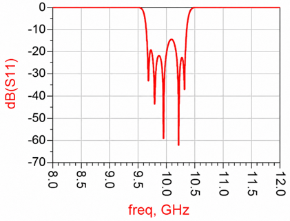
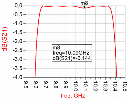
The simulation results in the ADS environment demonstrate an exceptional agreement with the design specifications after the final tuning process. Return Loss (S11): The filter achieved a significant return loss of approximately -21 dB at the center frequency of 10 GHz and -14.95 dB at the worst case [16, 17]. This high value indicates near-perfect impedance matching between the coupled stages and the 50 Ω ports, minimizing reflected power [18-20]. Insertion Loss (S21): Within the passband, the insertion loss was recorded at approximately -0.144 dB. This minimal loss confirms the efficiency of the microstrip configuration and the low-loss nature of the calibrated substrate [21]. Figure 2 illustrates these results.
The center frequency was precisely locked at 10 GHz. The achieved -3 dB bandwidth is 800 MHz, representing a fractional bandwidth of approximately 8% as seen in Figure 2. Although the initial target was 10%, the achieved bandwidth provides a higher selectivity, which is often desirable in X-band radar and modern digital communication applications to suppress adjacent channel interference [22, 23].
3.2 Impedance analysis
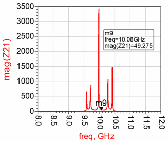
One of the most robust validations of this design is the impedance magnitude analysis across the 8-12 GHz range. As shown in the simulation plots: Identification of Poles: Five distinct resonant peaks are clearly visible within the passband. This confirms that all five resonators in the n = 5 design are active and correctly coupled. Resonance Stability: The markers (e.g., m3 at 10.08 GHz with 49.27 Ω) show that the impedance is extremely close to the characteristic impedance, ensuring maximum power transfer [24, 25]. The symmetrical distribution of these poles around the center frequency indicates a well-balanced coupling coefficient between the stages Figure 3 shows the impedance analysis.
Figure 3. Impedance analysis
3.3 The Voltage Standing Wave Ratio and loss factor analysis
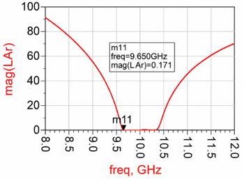
To further validate the impedance matching and power transmission efficiency, the voltage standing wave ratio (VSWR) and the Loss Factor LAr were calculated and analyzed. VSWR Analysis: The simulation results shown in Figure 4. Figure 4(a) illustrates that the VSWR value is consistently below 1.5 across the entire passband of 9.6 GHz to 10.4 GHz. At marker m5, 10 GHz, the VSWR is 1.44, which is an excellent result for high-frequency designs. A VSWR close to 1.0 indicates that the mismatch between the filter and the transmission line is negligible, ensuring that the maximum amount of signal power reaches the output port without being reflected [26]. Power Loss Factor LAr: The parameter LAr represents the attenuation or loss factor within the filter structure. As depicted in the results, the magnitude of LAr at the center of the passband (marker m6 at 9.65 GHz) is as low as 0.171. This minimal value confirms the high efficiency of the proposed parallel coupled configuration [9]. Furthermore, the results show the effectiveness of the dielectric constant calibration (εr = 3.39) in minimizing energy dissipation within the substrate. The consistency between the high isolation, the low VSWR, and the minimal loss factor provides an analytical correlation confirmation of the filter’s robustness. These results collectively demonstrate that the parasitic effects, which typically degrade performance in the X-band, have been successfully suppressed through the applied proposed methodology.
To assess the degree of achievement of the design goals, a comparison between the objectives and the outcomes obtained is shown in Table 4.
Table 4. Filter design performance summary
|
Parameter |
Design Target |
Simulated Result |
|
(f₀) |
10 GHz |
10 GHz |
|
Return Loss (S₁₁) |
< -10 dB |
-15 dB |
|
Insertion Loss (S₂₁) |
≈ 0 dB |
-0.2 dB |
|
Number of Poles |
5 |
5 |
|
Fractional Bandwidth |
10% |
8% |
In order to evaluate the filter's performance, the test results of the designed model were compared with the results of previous research. It was found through the comparison that the designed filter has a wide bandwidth to operate appropriately for modern communication systems, has a good matching factor, and the filter gain is constant over the operating range with an appropriate attenuation factor. Table 5 shows the comparison results.The competitiveness of the proposed filter for X-band frequency range is clearly presented in Table 5. A number of very recent reported designs have been selected to carry out the comparison, with the center frequency of the proposed filter fixed at 10 GHz. The proposed filter has the bandwidth of 800 MHz and low insertion loss, while the return loss is moderate. The proposed filter is a fifth-order parallel coupled microstrip structure, and this provides the best tradeoff between the required bandwidth, selectivity, and other parameters of the proposed design, i.e., the required selectivity, the insertion loss, and simplicity of the design. In the frame of the simulation-based designs of X-band microstrip bandpass filters, the proposed filter appears to be very competitive.
Table 5. Comparison with previous studies
|
Ref. |
f₀ GHz |
B.W. MHz |
S₁₁ dB |
S₂₁ dB |
Order |
Design Complexity |
|
[27] |
9.5 |
0.5 |
-10 |
-1 |
7th |
High |
|
[28] |
10 |
0.5 |
-23 |
-0.8 |
5th |
Moderate |
|
[29] |
8.5 |
0.4 |
-15 |
-0.7 |
2nd |
Low |
|
This Work |
10 |
0.8 |
-15 |
-0.2 |
5th |
Moderate |
This work has been limited to a numerical design. Hence, the behavior of the simulated ADS and the physically implemented ADS may differ due to implementation tolerances such as the dielectric constant of the substrate, surface roughness of the copper conductor, line width, slot width, line length, connection to the SMA port, soldering and the design of the measurement setup. This small difference may be shifted to the adjacent resonant frequency, increased Insertion Loss, and also may affect the impedance matching. The future work would be the implementation of the design and the measurement using vector network analyzer in order to verify the results.
In this paper a fifth-order X-band parallel coupled microstrip bandpass filter for 10 GHz operation frequency was designed and simulated by using the ADS software. In parallel coupled microstrip filters the center frequency of the filter is affected by the so-called parasitic fringing capacitance and by the additional effective electrical length of the coupled resonators. In the above design, these effects were compensated by using the Reverse Dielectric Calibrating approach (i.e., the effective dielectric constant of the substrate was decreased from 3.78 to 3.39 while keeping the above topology unchanged). The filter features an 800 MHz bandwidth corresponding to an 8% fractional bandwidth. In-band insertion loss and return loss are about −0.144 dB and −14.95 dB, respectively. The VSWR is below 1.5 within the passband. The plot of the impedance response of the filter features five resonant poles. The above design is simulation-based; therefore the implementation of the filter and the experimental verification of the simulated results is the subject of the future work.
The authors acknowledge the College of Engineering, University of Mosul for its support during the completion of this work.
|
Zoe |
Even Mode Impedances, Ω |
|
Zoo |
Odd Mode Impedances, Ω |
|
L S |
Transmission Line Length, mil Transmission Line Spacing, mil |
|
W |
Transmission Line Width, mil |
[1] Meyer, E., Vertegaal, C., Johnson, L., Meyer, P., Johannsen, U. (2023). Substrate integrated waveguide pedestal filtering-antenna and-arrays for 5G radio frequency front-ends. International Journal of Microwave and Wireless Technologies, 15(8): 1283-1290. https://doi.org/10.1017/S175907872300034X
[2] Nwajana, A.O., Arinze, S.N., Ebenuwa, S.H. (2025). Filtering antenna design and implementation techniques: Applications, recent developments, challenges, and future opportunities. Journal of Engineering, 2025(1): 8948687. https://doi.org/10.1155/je/8948687
[3] Ismael, A.A., Yaseen, M. (2025). Modified Doherty power amplifier with hybrid current-voltage amplification for high-efficiency broadband applications. International Journal of Robotics & Control Systems, 5(6): 3395-3412. https://doi.org/10.31763/ijrcs.v5i6.2172
[4] Paik, H., Premchand, K. (2023). Performance analysis of a single layer X-band frequency selective surface based spatial filter implementing half Jerusalem cross slot. Progress in Electromagnetics Research Letters, 108: 25-30. https://doi.org/10.2528/PIERL22091602
[5] Li, K.Y., Wu, Y.L., Lai, Z.G., Yang, Q.H., Wang, W.M., Yang, Y.H. (2024). Design of hybrid bandpass filter chips with high selectivity and wideband using IPD and FBAR technology. International Journal of RF and Microwave Computer-Aided Engineering, 2024(1): 9928016. https://doi.org/10.1155/2024/9928016
[6] Liang, G.Z., Chen, F.C. (2021). High selectivity filtering patch antenna using parasitic patches. In 2021 IEEE MTT-S International Wireless Symposium (IWS), Nanjing, China, pp. 1-3. https://doi.org/10.1109/IWS52775.2021.9499474
[7] Gruszczynski, S., Wincza, K. (2022). Extraction of parallel-coupled and end-coupled TEM resonator networks from a coupling matrix in the design of coupled-resonator filters. Electronics, 11(8): 1250. https://doi.org/10.3390/electronics11081250
[8] Chai, Y.Q., Zhang, X., Song, X.W., Hu, S.B., Liu, B.G., Liu, S. (2023). Synthesis design of wideband bandpass filter with high selectivity and harmonic suppression. IEEE Access, 11: 4173-4179. https://doi.org/10.1109/ACCESS.2023.3235730
[9] Hong, J.S., Lancaster, M.J. (2001). Microstrip Filters for RF/Microwave Applications. John Wiley & Sons. https://doi.org/10.1002/0471221619
[10] Pozar, D.M. (2012). Microwave Engineering, 4th Edition. John Wiley & Sons, Inc, pp. 26-30.
[11] Gruszczynski, S., Staszek, K., Wincza, K. (2023). Parallel-coupled bandpass filters with directly coupled input and output resonators. AEU-International Journal of Electronics and Communications, 172: 154974. https://doi.org/10.1016/j.aeue.2023.154974
[12] Gruszczynski, S., Wincza, K. (2024). Broadband impedance inverters for application in synthesis and realization of bandpass filters. IEEE Access, 12: 83260-83268. https://doi.org/10.1109/ACCESS.2024.3412148
[13] Mushtaq, B., Rehman, M.A., Khalid, S., Alhaisoni, M. (2024). Design of tri-band bandpass filter using modified X-shaped structure for IoT-based wireless applications. IEEE Embedded Systems Letters, 16(2): 194-197. https://doi.org/10.1109/LES.2023.3325898
[14] Li, C., Ma, Z.H., Chen, J.X., Wang, M.N., Huang, J.M. (2023). Design of a compact ultra-wideband microstrip bandpass filter. Electronics, 12(7): 1728. https://doi.org/10.3390/electronics12071728
[15] Ermis, S. (2024). The effect of substrate dielectric constant and thickness on millimeter wave band patch antenna performance. Celal Bayar University Journal of Science, 20(4): 40-59. https://doi.org/10.18466/cbayarfbe.1514216
[16] Akkader, S., Bouyghf, H., Baghdad, A., Belbachir, A.K., El Bakkali, M. (2024). Fabrication of compact substrate integrated waveguide dual band bandpass filter using complementary split-ring resonators for C and X band applications. e-Prime - Advances in Electrical Engineering, Electronics and Energy, 9: 100739. https://doi.org/10.1016/j.prime.2024.100739
[17] De, A., Roy, B., Bhattacharya, A., Bhattacharjee, A.K. (2021). Investigations on a circular UWB antenna with Archimedean spiral slot for WLAN/Wi-MAX and satellite X-band filtering feature. International Journal of Microwave and Wireless Technologies, 14(6): 781-789. https://doi.org/10.1017/S1759078721000891
[18] Taher, F., Fatah, S.Y.A., Mohamadien, K.H., et al. (2022). Design microstrip bandpass filter from 2 GHz to 4.7 GHz for biomedical applications. Journal of Advanced Research Design, 99(1): 1-9. https://akademiabaru.com/submit/index.php/ard/article/view/5225.
[19] Dawod, M.I., Hamid, K.H., Dheyaa, A., Fakhri, S.H.H., Yousif, M.I. (2025). Compact circular antenna with embedded coupled line filter for enhanced performance of 5G applications. Journal of Engineering Science and Technology, 20(5): 1554-1567.
[20] Paliwal, R., Srivastava, S., Budhiraja, R. (2024). Customizable substrate integrated waveguide based dual pole band pass filter for X band application. Progress In Electromagnetics Research M, 125: 11-19. https://doi.org/10.2528/PIERM24011002
[21] Pons-Abenza, A., Arregui, I., Laso, M.A.G., Lopetegi, T., Martin-Iglesias, P. (2024). Design of an additively-manufactured self-supported all-metal coaxial-line X-band bandpass filter. IEEE Access, 12: 68171-68183. https://doi.org/10.1109/ACCESS.2024.3399745
[22] Ali, H., Malik, B.T., Riaz, L., Shafique, M.F., Koziel, S. (2025). Multi-band frequency selective metasurface based filter for WLAN and X-band EMI shielding applications. Scientific Reports, 15: 22297. https://doi.org/10.1038/s41598-025-09056-1
[23] Zhao, K.C., Psychogiou, D. (2023). X-band MMIC-based tunable quasi-absorptive bandstop filter. IEEE Microwave and Wireless Technology Letters, 33(4): 391-394. https://doi.org/10.1109/LMWT.2022.3228572
[24] Popov, M., Xiong, Y., Zavislyak, I., Chumak, H., et al. (2023). Y-type hexagonal ferrite-based band-pass filter with dual magnetic and electric field tunability. Scientific Reports, 13: 1179. https://doi.org/10.1038/s41598-023-28279-8
[25] Pande, S., Patil, D., Kumar, A., Tyavlovsky, A., Muthanna, A. (2025). Design of a metasurface loaded with RF varactor and PIN diode integration dual-band reconfigurable antenna for bluetooth, Wi-Fi, WLAN and wireless 5G applications. Physica Scripta, 100(2): 025537. https://doi.org/10.1088/1402-4896/adac15
[26] Yang, M., Li, X.P., Bai, B.W., Li, Z., Xue, B.S. (2018). Transmission coefficient estimation based on antenna voltage standing wave ratio under plasma sheath. AIP Advances, 8(7): 075018. https://doi.org/10.1063/1.5038763
[27] Giribaldi, G., Colombo, L., Simeoni, P., Rinaldi, M. (2024). Compact and wideband nanoacoustic pass-band filters for future 5G and 6G cellular radios. Nature Communications, 15: 304. https://doi.org/10.1038/s41467-023-44038-9
[28] Bandar, H., Tokan, N.T. (2022). Comparison of post and iris substrate integrated waveguide band-pass filters for X-band applications. Sigma Journal of Engineering and Natural Sciences, 40(1): 45-56. https://doi.org/10.14744/sigma.2022.00004
[29] Bage, A. (2024). E-Plane dual band bandstop waveguide filter for possible X-band applications. International Journal of Electronics Letters, 12(3): 295-303. https://doi.org/10.1080/21681724.2023.2291809