Darshana N. Sankhe![]() | Snehal A. Bhosale*
| Snehal A. Bhosale*![]() | Neeraj Kumar Shukla
| Neeraj Kumar Shukla
© 2025 The authors. This article is published by IIETA and is licensed under the CC BY 4.0 license (http://creativecommons.org/licenses/by/4.0/).
OPEN ACCESS
DC-DC converters find extensive applications in renewable energy integration, electric vehicles, industrial machinery, medical devices, and various other fields. This work demonstrates Hardware-in-the-Loop (HIL) simulation of resonant inverter based DC-DC converter, with an implementation of discrete-time control system on Field-Programmable Gate Array (FPGA) platform. The proposed hybrid control strategy regulates the inverter’s output voltage/current using Phase Shift Controlled Pulse Width Modulation (PSC-PWM) with frequency tracking, along with maintaining the soft switching under dynamically changing load conditions. In this context, time-domain analysis is conducted to establish the relationship between inverter’s output voltage and load current, with respect to PSC-PWM duty ratio. HIL simulation is executed by creating an inverter simulation model in MATLAB-Simulink, while the control logic is developed using Xilinx System Generator for implementation on FPGA platform. The control system behavior is analyzed in real-time, for dynamically changing voltage, current, source and load conditions. An enhancement in performance of control system is assured by including the novel slope compensation technique with PSC-PWM control. Critical parameters like power consumption, hardware resource utilization, and timing details are evaluated for Zynq-XC7Z020-1clg484 and Artix-7 XC7A200T-2fbg676 FPGA platforms. These evaluations are essential in confirming the feasibility of proposed discrete-time controller and validating effectiveness of its implementation method on FPGA boards, mainly for industrial systems. Further, the proposed controller is tested experimentally on a laboratory prototype of 6 kW DC-DC converter.
DC-DC converter, discrete-time controller, FPGA, HIL, resonant inverter
Recent advancements in power semiconductor devices have spurred the adoption of controllers for the power systems through high-performance digital platforms. The commonly available digital platforms are microprocessors, microcontrollers, Digital Signal Processors (DSPs), and FPGAs. Among these platforms, microprocessors and microcontrollers have been popular due to their accessibility, cost-effectiveness, and user-friendly features. However, they often execute different control functions sequentially, resulting in a lower overall computational speed [1]. DSPs are specialized for mathematical operations but require substantial processing power and complex system architectures for the implementation of intricate control strategies. Moreover, DSPs execute various control tasks through software code and are thus less suitable for rapid execution of fast control algorithms. FPGA’s parallel architecture, reconfigurable and reprogrammable characteristics enable the development and rapid prototyping of controllers with minimal hardware modifications. Further, low latency, quick response time, and the afore mentioned characteristics make FPGAs particularly well-suited for real-time controller implementations. Also, the ASICs for power control applications can be quickly prototyped using FPGAs [2-6]. However, to-date these FPGA platforms are not easily and widely accepted in many power electronics control applications. Here, the major limitations of FPGA platform are observed as: (i) High cost of the FPGA boards over the traditional control platforms, (ii) Programming cost of firmware is also high due to the high skilled Hardware Description Language (HDL) programming requirement. Further, as the control algorithm complexity increases, the code development time for real-time control applications increases substantially and overall it becomes a time consuming task. To address these limitations, System Generator by Xilinx (now AMD) is being used that supports control system validation on FPGA hardware, in MATLAB-Simulink environment through HIL simulation [7-10]. Nowadays, these HIL simulation are prominently used in design, development, analysis and testing of industrial systems and many more applications because of its real-time validation capabilities, cost effectiveness, and rapid prototyping advantages for hardware systems [11-13].
Today, the resonant converters are commonly used because of their better efficiency, high power density, ability to operate at high switching frequencies, compact size, support to Zero Voltage and Zero Current Switching (ZVS/ZCS), and low Electromagnetic Interference (EMI) [14-17]. These resonant converters have different topologies like; (i) series, (ii) parallel, (iii) series-parallel converter etc. Among these topologies, the series resonant topology is widely used due to its simplicity and improved efficiency. But its output voltage regulation is difficult under no load condition and its maximum voltage gain is always less than unity, even at the resonant frequency [15, 18]. Thus, this topology is not suitable for the design of a DC-DC converter. The parallel resonant inverter possesses inherent short-circuit protection and better gain over series resonant topology but suffers from high circulating current and needs bi-polar switching [15, 18-20]. All benefits of series and parallel resonant topologies can be achieved by using a series-parallel resonant converter topology. Thus, in this work, a series-parallel resonant converter topology is chosen for implementation of a DC-DC converter. The DC-DC converters finds applications in; server power supply, EVs and hybrid-EVs battery chargers, smart grid to utility interface applications, telecom rectifiers, various renewable energy systems, electrolyzer applications etc. [21-28].
To avail all the benefits of the resonant inverters, the essential requirement is soft switching (i.e., ZVS and ZCS commutation of inverter switches), which requires continuous tracking of the resonant frequency. Traditionally, resonant frequency tracking is achieved by using an analog Phase Locked Loop (PLL) block. These PLL based systems perform well under constant load conditions, but fail to act under varying load situation. Hence, in this paper another approach of fast frequency tracking without using PLL block is used, as suggested by Calleja [29]. In this alternate approach, known as phase shifter and attenuation method, the switching frequency of resonant converter is always maintained above its resonant frequence, and ZVS is ensured at all load conditions.
Traditionally, the output power of resonant inverters is controlled by modifying the switching frequency. But it has a problem of handling EMI, requires complex filters and due to high frequency operation it exhibits low efficiency. To address these issues fixed-frequency control schemes like phase shift control and pulse width modulation control are preferred, but these techniques lose ZVS when resonant inverters are operated above wider output range. Here, to retain ZVS at all output levels, the switching frequency must be kept very high above the resonant frequency, but this will reduce the inverter efficiency. Thus for better efficiency, inverters should be operated slightly above the resonant frequency. To achieve this, resonant frequency tracking is used and inverter is always operated at slightly higher frequency above the resonance. This solves the basic limitation of fixed-frequency control schemes. Therefore, in this work combination of phase shift and pulse width modulation with frequency tracking scheme is preferred. Further, the output voltage and load current regulation of a DC-DC converter is a function of the inverter switching frequency and PSC-PWM duty ratio. This modification of PSC-PWM duty ratio and switching frequency simultaneously, for varying load conditions is achieved using hybrid control strategy discussed in studies [30-32]. This work is explored further in this paper for the analysis and development of controller for constant voltage and constant current DC-DC converter.
In Section 2, the series-parallel resonant inverter-based DC-DC converter is designed, and its time-domain analysis is carried out to investigate the relationship between its input-output control variables. The design and implementation of control strategy for constant voltage and constant current DC-DC converter is covered in Section 3. In Section 4, HIL simulation and experimental results are presented for dynamic load and source conditions, and Section 5 covers conclusion.
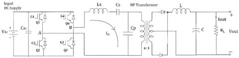
The power stage configuration of conventional series-parallel resonant inverter used in a DC-DC converter is shown in Figure 1. In this setup, the input from AC mains is rectified and filtered using capacitive filter to produce a stable and smooth DC bus voltage, Vdc. A H-bridge series-parallel resonant inverter is composed of four IGBT switches (Q1, Q2, Q3 and Q4) and a LCC resonant tank.
Figure 1. Power circuit of DC-DC converter
The four switches in this circuit operate at 50% duty ratio and the switch in each leg synchronously operates 180° out of phase. To prevent undesirable cross-conduction, a slight dead-time is introduced between the switching cycles of these complementary switches. In order to introduce a phase shift between two opposite legs, pulse width modulation is applied. This modulation stage is connected through a high frequency transformer to a rectifier bridge, filter and rated load, for isolation as well as the voltage or current scaling. The intermediate LCC resonant tank network between H-bridge inverter (modulation stage) and rectification stage, exhibits inherent AC gain, that is function of switching frequency and PSC-PWM duty ratio. Control of these two parameters thus allows output voltage and load current regulation, as they determine the input of rectifier based on different loading conditions. This modification of PSC-PWM duty ratio and switching frequency simultaneously is achieved using hybrid control strategy, discussed in section 3.
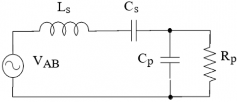
In DC-DC converter the rated load RLis connected across rectifier bridge along with a L-C filter as shown in Figure 1. Here, the non-linear behavior of rectifier modifies the equivalent load resistor loading LS-CS-CP tank. This AC equivalent load resistance, RPreflected at the primary of high-frequency isolation transformer is given as:
$R_P=\frac{n^2 \pi^2 R_L}{8}$ (1)
(a) AC equivalent of LCC resonant converter
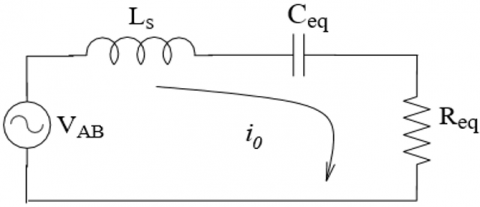
(b) Equivalent series LCR resonant circuit
Figure 2. Equivalent circuit of DC-DC converter as seen from primary side of matching transformer
where, n is the transformer turns ratio. If inverter output voltage is represented as VAB, then the resultant AC equivalent circuit for LCC loaded resonant converter is as shown in Figure 2(a). Here, the parallel branch (RP-CP) is further represented into its equivalent series component, to constitute a series RLC resonant circuit as depicted in Figure 2(b). Here, the corresponding resistance, Req and capacitance, Ceq are evaluated as:
$R_{e q}=\frac{R_p}{1+A}$ (2)
$C_{e q}=\frac{C_s C_p\left(1+\frac{1}{A}\right)}{C_s+C_p\left(1+\frac{1}{A}\right)}$ (3)
where, A=(RpCpω)2. The natural resonant frequency of this series LS-Ceq-Req resonant load is given as:
$f_0=\frac{1}{2 \pi \sqrt{L s C_{e q}}}$ (4)
Applying Kirchhoff’s voltage law to above circuit gives:
$V_{A B}(\mathrm{t})=L_s \frac{d i_o(t)}{d t}+\frac{1}{C_{e q}} \int i_o(t) d t+i_o(t) R_{e q}$ (5)
where, VAB(t) is inverter output voltage, a quasi-square waveform. If its fundamental frequency voltage VAB1(t) is considered, then the value of VAB1(t) in terms of PSC-PWM duty ratio d is given as:
$V_{A B 1}(\mathrm{t})=\frac{4 V_{d c}}{\pi} \sin \left(\frac{\pi}{2} d\right) . \sin \omega t$ (6)
where, Vdc signifies the DC bus voltage, and ω represents the inverter’s fundamental input switching frequency.
The connection between the duty ratio, load current and an output voltage is established by analyzing the integro-differential equation and subsequently solving it to determine the expression for i0(t). By taking into account VAB(t) as the input excitation for the series Ls-Ceq-Req circuit illustrated in Figure 2(b) the time-domain expression for the resulting current, denoted as i0(t) can be derived as follows:
$i_o(t)=\frac{V_{m 1} \cdot \omega}{L_s}\left\{i_{s s}(t)+i_{t r}(t)\right\}$ (7)
$i_{s s}(t)=\frac{1}{x^2+y^2}\{x~cos~\omega t+y~sin~\omega t\}$ (8)
$\begin{gathered}i_{t r}(t)=K\left\{\left(b_0 p-a_0 q\right) \cos b_0 t-\left(a_0 p\right.\right. \left.\left.+b_0 q\right) \sin b_0 t\right\}\end{gathered}$ (9)
where, ${{V}_{m1}}$=$\frac{4{{V}_{dc}}}{\pi }\sin \left( \frac{\pi }{2}d \right)$; $x=a_{0}^{2}+b_{0}^{2}-{{\omega }^{2}}$; y=2a0ω; K=$\frac{{{e}^{-{{a}_{0}}t}}}{{{b}_{0}}\left( {{p}^{2}}+{{q}^{2}} \right)}$; p=$a_{0}^{2}-b_{0}^{2}+{{\omega }^{2}};$ q=2.${{a}_{0}}.{{b}_{0}};{{a}_{0}}=\frac{{{R}_{eq}}}{2{{L}_{s}}}$;$~{{b}_{0}}={{\omega }_{0}}\sqrt{1-1/\left( 4{{Q}^{2}} \right)}$ and ${{\omega }_{0}}=\frac{1}{\sqrt{{{L}_{s}}.{{C}_{eq}}}}$.
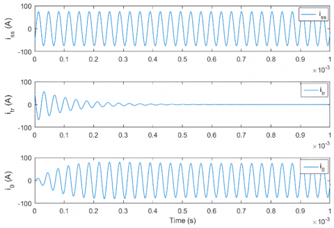
Figure 3. Plot showing steady state, transient and resultant load current of LCC resonant inverter across Cp−Rp branch
Eq. (7) defines the current with two distinct components: the steady-state component, iss(t), and transient component, itr(t). In Figure 3, the time-domain plot of i0(t) illustrates the transient behavior of the resultant current before it settles into a steady state. This resonant current is referred for deciding the required IGBT current ratings as well as the L and C components, in the design of practical LCC resonant inverter-based systems. The steady state component of current, iss(t) and output voltage, Vout are considered to calculate the voltage gain (AV) as:
$V_{\text {out }}=i_{s s}(t) . Z_p$ (10)
$A_v=\frac{V_{{out }}}{V_{d c}}$ (11)
where, Zp is an equivalent impedance of CP−RP branch as shown in Figure 2(a). Further the load current through reflected ac resistor IRp is evaluated as:
$I_{R p}=i_{s s}(t) .\left|\frac{x_{C p}}{x_{C p}+R_p}\right|$ (12)
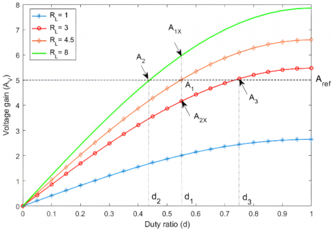
Figure 4 illustrates the relation between voltage gain and duty ratio for different values of load resistor (RL), for normalized switching frequency ωn=1.05, where ωn=ω/ω0. To evaluate the process of regulating voltage gain by duty ratio control, consider that required voltage gain is Aref=5. At RL=4.5 Ω the voltage gains A1=Aref is achieved at duty ratio d1. Now, if the load increases to RL=8 Ω then accordingly gain increases from A1 to A1X when duty ratio d1is maintained at the same value. Here, the controller reduces the duty ratio from d1 to d2, to maintain Aref as the reference value, effectively restoring the gain to the desired reference level A1. Similarly, if the load decreases from RL=4.5 Ω to say RL=3 Ω then gain drops from A1 to A2X with the same duty ratio d1. Here, the duty ratio is increased from d1 to d3 and the gain is regulated to A3 as per the reference level requirement. In this way the required voltage gain can be regulated by modifying the duty ratio. Here, it is observed that if RL drops to a very low value, then gain drops accordingly to lower level. In this case, achieving required voltage gain is not possible as the controller enters into a constant current mode of operation.
Figure 4. Voltage gain as function of duty ratio with various RL, ωn=1
Similar to this, the procedure for controlling and regulating the load current through duty ratio control can be analyzed. In all, the controller regulates both inverter output voltage and load current dynamically by adjusting the duty ratio, on the basis of load resistance. In doing so, the controller should modify the switching frequency to ensure soft switching condition.
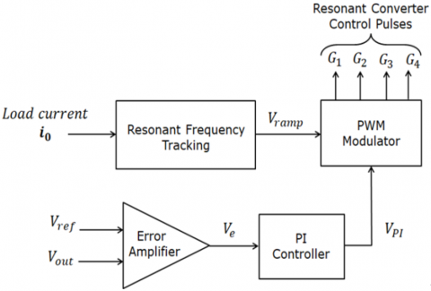
The primary objectives of the proposed controller structure are: (i) To maintain a consistent output voltage, (ii) Another critical function is to sustain ZVS throughout a wide range of load conditions. This helps to minimize switching losses and enhances operational efficiency. (iii) To optimize the inverter’s power factor and overall efficiency, by operating the inverter near its resonance point.
Figure 5. Constant voltage DC-DC converter controller
In this design, achieving precise output voltage regulation necessitates dynamic adjustments of PSC-PWM duty ratio. However, altering the duty ratio without corresponding changes in the switching frequency can lead to ZVS loss. To overcome this challenge, real-time tracking of the resonance frequency becomes essential, enabling the controller to adapt the duty ratio in accordance with the desired output voltage. Here, controller changes the inverter’s switching frequency simultaneously so that soft switching conditions are maintained. To fulfill these complex requirements, a sophisticated control strategy has been developed, comprising of two major control loops as shown in Figure 5:
(i) Resonant Frequency Tracking (RFT): This loop continually monitors and tracks the resonance frequency, ensuring that the inverter operates near its resonant point.
(ii) Output Voltage Control Loop: Concurrently, this loop manages the regulation of the output voltage by dynamically adjusting the PSC-PWM duty ratio in response to the desired output voltage.
3.1 Voltage control loop design
In the design of voltage control loop, at first the set reference voltage, Vref is compared with measured output voltage, Vout to obtain an error signal, Ve. This error in voltage signal is further compensated by discrete-time Proportional-Integral (PI) controller. The PI controller’s discrete-time equation is derived using bilinear transformation as:
$\begin{aligned} V_{P I}(n)= & V_{P I}(n-1)+\left(K_p+\frac{K_I . T_s}{2}\right) V_e(n)+ \left(\frac{K_I . T_s}{2}-K_p\right) V_e(n-1)\end{aligned}$ (13)
where, Kp, KI are PI controller’s gains, Ve is voltage error, Ts is the sampling time and VPI is the final output of PI controller. The control signal obtained through this PI controller further modifies the duty ratio of resonant inverter using a PSC-PWM generation block (i.e., PWM Modulator). The gains of the PI controller are tuned accordingly, to achieve the required control action.
Table 1. DC-DC converter parameters
|
Description |
Parameter |
Value |
|
Nominal DC input supply voltage range |
Vdc |
450-700 V |
|
DC input supply voltage |
Vdc |
600 V |
|
Series inductor |
LS |
370 µH |
|
Series, parallel capacitor |
CS, CP |
0.22 µF |
|
Load resistor (rated) |
RL |
2.4 Ω |
|
Frequency range |
F0 |
25-30 kHz |
|
Transformer turns ratio |
N = NP / NS |
4.0 |
|
Rated output power |
Pout |
6 kW |
|
Rated inverter kVA |
- |
7.2 kVA |
|
Output voltage range |
Vout |
110-135 V |
|
Nominal output voltage |
Vout |
120 V |
|
Nominal output current |
Iout |
50 |
In order to assess the PI controller gains and examine the stability of the control system, it is essential to derive an approximate process plant model. The input-output variables of this plant model are, duty cycle controlling voltage, VPI, and DC output voltage, Vout. The continuous-time and discrete-time transfer functions of the plant model are given in Eq. (14) and (15) respectively, for the equivalent circuit in Figure 2 and the circuit parameters as mentioned in Table 1.
$G(s)=\frac{K_v}{\left(1+2 \zeta . T_\omega . s+\left(T_\omega . s\right)^2\right)\left(1+T_{p 3} . s\right)}$ (14)
$G(z)=\frac{5.931 .10^{-27}+1.779 .10^{-26} z^{-1}+1.779 .10^{-26} z^{-2}+5.931 \cdot 10^{-27} z^{-3}}{1-3 z^{-1}+3 z^{-2}-z^{-3}}$ (15)
where, Kv=352.2, $T_\omega$ =141.67, ζ=0.3773 and Tp3=369.85. This open loop plant model is naturally unstable and requires PI compensator to achieve the desired control action. Here, PID-tuner software application in MATLAB is used and PI controller’s gains are obtained as; Kp=1.152×10⁻³ and KI=4.5167×10⁻⁶. With these gains, at the prominent load conditions, simulation of this system works well with rising time of 702 µs, settling time of 1644 µs, and overshoot of 0.46%. The bode plot of this compensated system gives stability margins as: gain margin, GM=12.2 dB and phase margin, PM=72°. The PWM modulator block continuously compares the PI controller’s output, VPI with the ramp signal, Vramp obtained from frequency tracking loop and generates the phase shifted switching control pulses (G1−G4), for LCC resonant inverter switches (Q1−Q4) respectively.
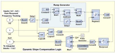
3.2 Dynamic slope compensation logic
In the design of RFT loop, phase-shifter and attenuator, comparator and integrator blocks are used. During each inverter cycle, the output of an integrator block (i.e., ramp signal, Vramp) and voltage PI controller’s output (VPI) are processed by a PWM modulator block and accordingly the inverter control pulses G1–G4 are generated. Here, control pulses G1 and G2 are complement of each other. Similarly, G3 and G4 are complementary. A PWM modulator block introduces a phase shift between G1 and G3 based on the received inputs (Vramp and VPI). This phase shift directly controls the pulse width and regulates the ON time of the resonant inverter. Now, if the slope of ramp signal in an integrator block is kept constant, then with the shift in switching frequency, the peak of ramp signal will vary which results in the identical phase shift between G1 and G3 even though the switching frequency has changed. This will affect the linearity of the voltage control loop. Further, in some cases the ramp signal peak may not reach to its maximum value (i.e. unity) or may remain below the PI’s output signal, particularly in low output regions. This leads to unpredictable phase shifts between G1 and G3 or even controller failure.
To address these challenges, a Dynamic Slope Compensation (DSC) logic is proposed, wherein the slope of the ramp signal is dynamically adjusted in each inverter cycle, based on the switching frequency. This ensures that ramp peak will always reach to maximum value (unity) at all frequencies and output conditions, maintaining a proportional phase shift between G1 and G3 pulses. As a result, the inverter ON time is synchronously adjusted, improving the linearity of the control system and preventing potential controller failures.
3.3 Controller design in XSG
To facilitate the controller implementation onto the FPGA platform, the entire control system needs to be designed using Xilinx System Generator (XSG) block sets. Here, each sub-system is designed using various elementary, logical, control, mathematical and MCode blocks. The detailed design of DSC logic using XSG block sets is covered here. DSC logic is basically used to modify the slope of a ramp signal generated by an integrator block in the RFT loop (Figure 5). In design of this DSC logic using XSG block sets, a sample and hold concept is used. Its implementation using various logical, arithmetic operators, multiplexers, register, counter, reciprocal, and delay blocks is shown in Figure 6. To calculate the slope constant for the preceding integrator blocks, it processes the received comparator block outputs from the frequency tracking loop and generates the reference ramp signal. Here, at the start of each inverter cycle, the ramp generator is initialized to zero and it increments further with the constant slope. The peak of this ramp signal is sampled at the end of each cycle and stored in the register block. Network of logical and delay blocks generate the synchronous enable pulses for this register block, at the end of each cycle.
Figure 6. DSC logic design with XSG block sets
Further, a reciprocal of the peak value is evaluated which is used as a slope constant by the integrator unit. Any change in the inverter resonant frequency results into the variation in the peak value of the ramp, which modifies the slope constant in such a way that the integrator’s output will always reach a unity value. This brings linearity in the control system as well as improves the response time of the control system [32]. At the start of the simulation, multiplexer is used to start the integrator with a constant slope, initially for 1000 cycles and once the desired current oscillations are developed, then it switches to the proposed dynamic slope. Here, maximum control structures are implemented using the fixed-point representation but at the selected places floating-point representation is also used. For example, in the implementation of reciprocal block it is must to use floating point data representation. This reciprocal operation supports only two formats: single precision and double precision floating-point representation. Therefore, at this point the cast block is used to convert fixed-point format into single precision floating-point format and reciprocal operation is performed. The result of this block is converted back into fixed point format for further processing, again using a cast block. It is observed that for some operations this floating-point representation generates desired results quickly whereas, fixed-point formats showed increase in size with consecutive cycles and hence adds latency [9].
To validate the controller design on FPGA platform, first a complete system MATLAB-Simulink model was developed, and performance was verified using simulations. Further, the controller model was developed using XSG block sets, while keeping electrical system model in MATLA-Simulink and again performance was verified using simulations. Finally, the HIL simulation was carried out by implementing controller onto the FPGA platform. As illustrated in Figure 7, the HIL simulation system configuration comprises of Zynq XC7Z020-1clg484 FPGA-Board, interfaced with computer system using JTAG cable. There are two ways to interface the FPGA boards to personal computer (XSG): (i) Ethernet (point-to-point) and (ii) JTAG. The point-to-point Ethernet interface supports 10/100/1000 Gbps connection and uses IPv4 network infrastructure. The JTAG co-simulation interface uses minimal resources on FPGA and hence used as a common interface technique. The FPGA operates at a clock frequency of 100 MHz, facilitating the seamless interfacing and optimal functioning of all sub-systems as per their intended specifications. The complete control system is implemented on the Zynq-XC7Z020 FPGA board using the XSG Controller Model, within a HIL simulation framework.
Figure 7. HIL simulation system configuration
In order to obtain the HIL simulation results closer to an experimental set-up we have referred to the IGBT (SKM200GB125D) data sheet and have modelled IGBT parameters accordingly. Typical on-state resistance across collector-emitter terminal of IGBT was set as RCE=0.012 Ω, and snubber resistance RS=100 kΩ. Further, in design of power systems, the inverter switches (IGBTs) are operated at few kilohertz frequencies. Therefore, to attain the accurate results in such power systems, very small time step is required. In literature, the recommended time step for design of power converters is smaller than or equal to 1µs [33]. Thus, a sampling time of Ts=0.1 µs has been selected for the experimentation. For HIL simulation, the electrical parameters outlined in Table 1 are considered.
The proposed controller performance was evaluated through HIL simulation on Zynq XC7Z020-1clg484 Evaluation and Development Board. FPGA resources utilized for DC-DC converter’s controller implemented on Zynq board are: 2 BRAM’s, 44 DSP’s, 2337 LUT’s and 1527 Registers. For timing and power analysis of the design on FPGA board, the HDL code of control logic was executed on Xilinx Vivado Design Suit software. After synthesis the power dissipation was 0.19W and timing reports gives worst case negative slack 2.1 ns. This ensures that FPGA can be operated at higher speed/frequencies, which cannot be achieved easily by using traditional hardware’s like: DSP/CPU/Microcontrollers based systems.
The controller performance was further evaluated through HIL simulation on the Artix-7 XC7A200T-2fbg676 evaluation board. Here, the resources utilized were; 2 BRAMs, 44 DSPs, 2107 LUTs and 1985 Registers. The power dissipation was 0.15 W and worst negative slack was 1.32 ns. Here, the resource utilization remained similar in both cases because the controller design was synthesized into the FPGA, and both boards had 28 nm technology with a similar FPGA fabric. However, some variations in LUTs and Registers are observed due to differences in FPGA architecture and routing. Artix-7 XC7A200T-2fbg676 has higher speed grade hence it’s a faster device compared to the Zynq XC7Z020-1, leading to an improvement in the timing performance. Additionally, Artix –7 is pure FPGA having only programmable logic, no built-in processor, and it is optimized for low power. As a result, the design implemented on the Artix-7 exhibited lower power dissipation compared to the Zynq board.
The following section covers the results obtained from HIL simulation for both constant voltage and constant current DC-DC converter.
4.1 Constant voltage DC-DC converter
In this sub-section, the overall system performance of constant voltage DC-DC converter is verified through HIL simulations, with the controller implemented on FPGA board, for different parametric conditions. Also the experimental results are presented.
4.1.1 Output voltage variation
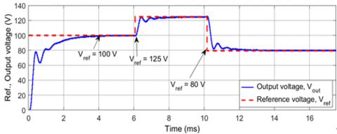
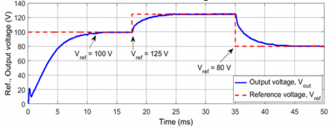
To evaluate the dynamic performance of the proposed controller, a comprehensive set of experiments was carried out, and the controller’s response to these changes is observed and analyzed. In the initial step, the reference voltage (Vref) was set at 100 V. From the inception of simulation, the controller tracks the reference voltage and achieved a stable state within a period of just 4 ms.
Subsequently, in the second step, the reference voltage was altered from 100 V to 125 V. As anticipated, the actual output voltage followed set reference voltage, transitioning smoothly from 100 V to 125 V, and it promptly stabilized, achieving a steady state in just 2 ms. The third step-change occurred at the 10.2 ms mark, reducing the reference voltage from 125 V to a lower value of 80 V. In this scenario as well, the actual voltage adeptly tracked the reference voltage, and within a mere 2 ms, it settled at a steady-state output voltage of 80 V. Throughout these voltage reference changes, we observed that the controller effectively adjusted the PWM duty ratio to accommodate the variations. Importantly, the controller maintained ZVS across all voltage levels through its frequency control mechanism. In Figure 8(b), it becomes evident that in the absence of the DSC logic, controller requires significant time to trace and stabilize the output at set reference voltage levels.
(a) With DSC logic
(b) Without DSC logic
Figure 8. Step transient response of controller at R=2.4 Ω with Vref=100 V, 125 V, 80 V
4.1.2 Load resistance variation
Under the dynamic load conditions, the performance of proposed controller is evaluated by introducing a change in the output resistance, both with and without the DSC logic. These tests were carried out while maintaining a constant reference voltage (Vref) at 120 V. Initially, with the reference voltage set at 120 V, the controller tracked this value and achieved a stable state within a 2 ms. At the 6 ms mark, we introduced a change in the load resistance, reducing it from 24 Ω to 2.4 Ω. This alteration in load resistance caused the output voltage of the system to decrease from 120 V to 80 V, as illustrated in Figure 9(a). In response to this drop in load resistance, the controller promptly adjusted the PWM duty ratio and effectively tracked the reference voltage in just 4 ms. The voltage drop appears to be nearly identical in both scenarios, as depicted in Figure 9(b). However, it is seen that the settling time is significantly high for controller without DSC as compared to the controller equipped with DSC logic.
(a) With DSC logic
(b) Without DSC logic
Figure 9. Step transient response of controller at Vref=120 V with R=24 Ω, 2.4 Ω
4.1.3 Source variation
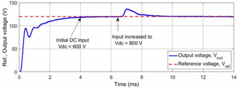
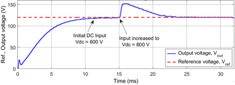
In order to assess the performance of the proposed controller under varying source conditions, we conducted experiments involving changes in the DC bus voltage. These experiments were carried out both with and without the DSC logic, while maintaining a constant reference voltage (Vref) of 120 V and an output resistance (R) of 2.4 Ω. Initially, with the reference voltage set at 120 V, the controller efficiently tracked this value and achieved a stable state within 4 ms. Subsequently, we introduced a change in the input DC bus voltage (Vdc), increasing it from 600 V to 800 V. This abrupt increase in the DC bus voltage led to an increase in the system’s output voltage from 120 V to 135 V, as depicted in Figure 10(a). In response to this sudden increase in the DC bus voltage, the controller swiftly reduced the PSC-PWM duty ratio, effectively tracking the reference voltage in just 2 ms.
(a) With DSC logic
(b) Without DSC logic
Figure 10. Step transient response of controller at Vref=120 V, R=2.4 Ω with Vdc=600 V and 800 V
Similarly, when there is a sudden decrease in the DC bus voltage from 600 V to 450 V, it causes the system’s output voltage to drop from 120 V to 105 V. In response to this abrupt voltage drop, the controller increases the duty ratio and effectively tracks the reference voltage within a span of 3 ms. In all, during the operational cycle of a DC-DC converter, abrupt changes in the DC bus voltage can result in rapid increases or decreases in the output voltage. These voltage variations are substantial and require more time to align with the reference voltage level in controllers that lack the DSC logic.
4.1.4 Effects of dynamic slope compensation logic
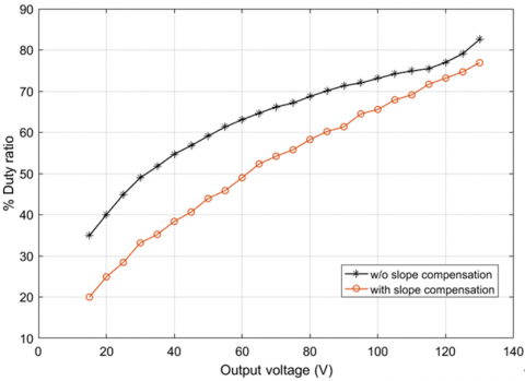
To assess the impact of DSC logic, we conducted experiments by varying the reference voltage within the range of 15V to 135V. These experiments were conducted under consistent control parameters and circuit conditions within a closed-loop control system. Figure 11 displays the plot of steady-state values of the output voltage as a function of duty ratio, allowing us to draw the following conclusions:
1. Linear Relationship with DSC: When the DSC is employed, the relationship between the duty ratio (d) and the output voltage is linear across most of the voltage range, in contrast to the case without DSC. This linearity enhances the controller’s precision in achieving the desired control objectives.
2. Extended Voltage Control Range: With the DSC implementation, the range of duty ratio needed to encompass the specified voltage range is notably wider when compared to the scenario without DSC logic. Consequently, the voltage control range is enhanced when using DSC logic.
Figure 11. Plot of average output voltage vs. duty ratio with DSC and without DSC logic
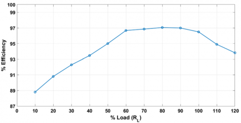
Figure 12. Efficiency plot
To investigate the efficiency of DC-DC converter, a simulation is carried out with the bus voltage regulated at Vdc=600 V, a reference voltage set to 120V, and a reference current set to 50A. The load resistor (RL) is varied gradually from 10% to 120% of the rated load. The corresponding input and output average power are measured, efficiency is calculated and plotted as shown in Figure 12. The results indicate that efficiency reaches its peak at 80% of the rated load condition and gradually decreases at both, lower and higher load conditions. Since the efficiency is evaluated at steady-state input-output conditions, the DSC logic has not impacted the overall converter efficiency.
The results obtained from HIL simulations confirm that the performance of constant voltage DC-DC converter controllers is significantly improved through the incorporation of the newly introduced DSC logic.
4.1.5 Experimental results
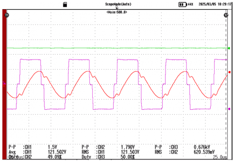
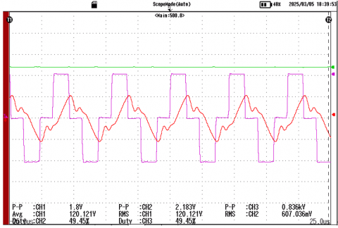
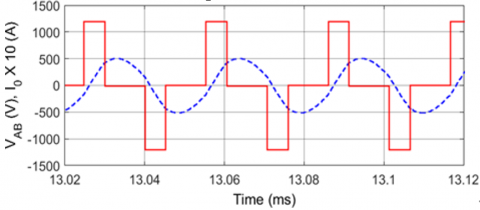
To validate the performance of control system, an experimental set-up of DC-DC converter is built as shown in Figure 13, with the specifications listed in Table 1. The system consists of IGBT-based H-bridge LCC resonant inverter, followed by a synchronous rectifier, filter, and resistive load. Here, to safeguard the controller and oscilloscope from high-voltage spikes and circulating currents, an isolator is used to electrically isolate the power stage ground. Figure 14(a) presents the inverter output voltage and resonant current waveforms for output voltage (Vout) of 120V, at input DC bus voltage (Vdc) of 300V. Here, the resonant current is sinusoidal and leads the inverter voltage, ensuring ZVS. Figure 14(b) shows waveforms for Vout=120V at an increased input Vdc=500 V, here it is observed that as per the input conditions the PWM duty ratio is adjusted and required output is achieved. In experimental set-up, stray parameters exist those results in ringing on voltage and current waveforms. These ringing effects are not observed in HIL simulation results in Figure 18, due to the idealized nature of the simulation environment.
Figure 13. Experimental set-up for DC-DC converter
(a)
(b)
Figure 14. Converter output (green trace), inverter output voltage (purple trace), and resonant current (red trace) waveforms at (a) Vdc=300 V, (b) Vdc =500 V
4.2 Constant current DC-DC converter
To test the real-time performance of the constant current DC-DC converter control system, the HIL simulation is carried out using the developed HIL test-bench. Through the obtained HIL simulation results of constant voltage DC-DC converter, it has been observed that introducing DSC logic has improved the overall control system performance. Similar performance improvement is observed even in case of constant current DC-DC converter. Hence, for all further simulations we have considered the controller with DSC logic and accordingly the results are presented, for different parametric variations.
4.2.1 Output current variation
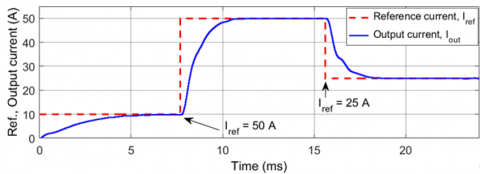
To evaluate the tracking performance of the control system, the reference current is varied in the three steps, at identical parametric conditions. Initially the reference current was set to 10 A. The controller tracks the reference current in 5.5 ms. as shown in Figure 15. At T=7.7 ms reference current is increased to 50 A, here the controller proportionally modifies the inverter output and attains the reference set value in around 3 ms. Next, step change in reference current is introduced at T=15.5 ms and reference current is reduced to a low value of 25 A. Here also the controller tracks the reference set value in just 3 ms with gradual reduction in inverter output parameters. As discussed earlier, with decrease in the duty ratio, ZVS will be lost if the resonant inverter is operated with fixed frequency. Hence, this controller continuously increases the switching frequency for the proportional decrease in the duty ratio and maintains ZVS throughout the operating range of the control system.
Figure 15. Step transient response of controller at Vdc=600 V, R=2.4 Ω with Iref=10 A, 50 A, 25 A
4.2.2 Load resistance variation
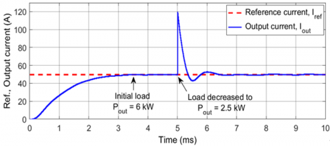
To analyze the step transient response of the control system under different load conditions, we introduce a step change in the output power. Here, the output power was initially set to Pout=6 kW, and at T=5 ms this power is changed to Pout=2.5 kW. As shown in Figure 16, step change in power increases the output power drastically to 14.5 kW, but with the close loop corrective action of the control system, the output power gets regulated to required power level (2.5 kW) in 1.5 ms.
Figure 16. Step transient response of controller at Iref=50 A, Vdc=600 V with Pout=6 kW and 2.5 kW
4.2.3 Source variation
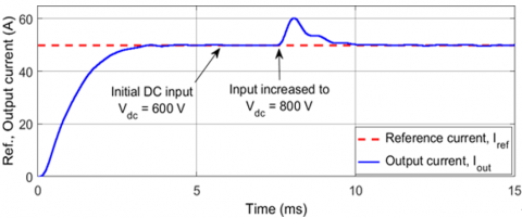
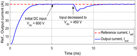
The performance of proposed controller under fluctuating source conditions is verified by changing the dc bus voltage from 600 V to 800 V and 450 V respectively as shown in Figure 17. These sudden changes in the dc bus voltage results into sudden increase or drop in the output current. Here, controller varies the PWM duty ratio and tracks the reference current level, Iref=50 A within 2.5 ms. To analyze this variation in the PWM duty ratio, two extreme conditions of dc bus voltage variation are considered here. Figure 18 depicts resonant converter’s output voltage and load current waveforms for different dc bus voltage levels, with identical parametric conditions.
(a) Input Vdc=600 V and 800 V
(b) Input Vdc=600 V and 450 V
Figure 17. Step transient response of controller at Iref=50 A, R=2.4 Ω and varied inputs
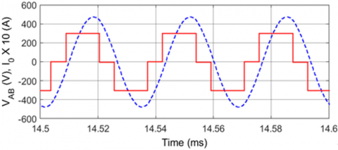
In case of very low input voltage, Vdc=300 V the controller increases the PWM duty ratio d=69 % and attains the reference current level. Here, the switching frequency is observed to be fs=29.8 kHz (Figure 18(a)). As the input increases to Vdc=1200 V, the controller automatically decreases the PWM duty ratio to d=34 % as shown in Figure 18(b) and regulates the required output current level. At this point, the frequency is observed to be fs=32.6 kHz. Here, it should be noted that with the decrease in the duty ratio, the frequency should be increased proportionally, otherwise ZVS will be lost.
(a) Input Vdc=300 V
(b) Input Vdc=1200 V
Figure 18. Resonant converter’s output voltage and load current waveforms at Iref=50 A, R=2.4 Ω and varied inputs
4.2.4 Output current vs. duty ratio
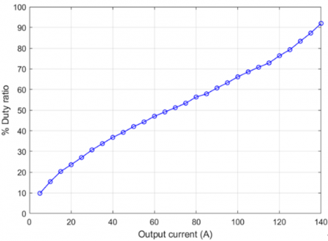
To investigate the safe operating range of this control system/current source, the output current is varied in the range of 5 A to 140 A, and the relationship of output current verses duty ratio is plotted as shown in Figure 19. Here, it is observed that the required output current range of 5 A to 140 A is maintained by varying the PWM duty ratio in the range 9.7% to 92%. In all experimental systems, the preferred operating duty range is between 20% to 80%. Thus, this current source can be safely used for all real-time applications within the specific output current range. These HIL simulation results perfectly validate the functionality of developed control strategy for both; constant voltage and constant current DC-DC converters. Overall, these outcomes validate both the viability of the control strategy and the efficacy of its implementation onto the FPGA platform.
Figure 19. Plot of average output current vs. duty ratio
The series-parallel resonant inverter-based DC-DC converter has been designed to operate seamlessly as both, a constant voltage and constant current DC-DC converter. Time-domain analysis is carried out to investigate the dependences between input-output control parameters. A unified hybrid control strategy has been proposed and successfully implemented on the FPGA platform. An incorporation of DSC logic has showed enhancement in performance of controller over the conventional PSC-PWM control method. Performance analysis at dynamic voltage, current, load and source conditions has showed improvements in response times by 55% and reduction in overshoots by 15% at the system output. Also, the voltage and current control loop linearity has been enhanced. HIL simulation results show that for output voltage/current variation in the range 25% to 100%, the required PSC-PWM duty ratio variation is observed to be 30% to 75%, whereas the resonant inverter’s switching frequency varies only by 2.8 kHz to retain ZVS condition. The experimental results show regulation of output voltage at varied input conditions by proportionally modifying the duty ratio and parallelly maintaining ZVS.
The HIL simulation platform discussed here is proven to be a highly efficient validation tool for the development and testing of discrete-time controllers on FPGA platforms. The results from HIL simulations affirm the effectiveness and practicality of implementing discrete-time control systems on the FPGA platform. Importantly, the resource utilization analysis of the proposed controller architecture indicates its suitability for deployment on lower-version and cost-effective Artix FPGA platforms. This controller could be useful for prominent DC-DC converter applications such as: chargers for EV’s and Hybrid EV’s, Photo-voltaic systems, Fuel cell systems, Electrolyzer applications, high-power industrial systems, telecom rectifiers etc., with implementation on FPGA board.
[1] Sepúlveda, C.A., Muñoz, J.A., Espinoza, J.R., Figueroa, M.E., Baier, C.R. (2012). FPGA v/s DSP performance comparison for a VSC-based STATCOM control application. IEEE Transactions on Industrial Informatics, 9(3): 1351-1360. https://doi.org/10.1109/TII.2012.2222419
[2] Bahri, I., Idkhajine, L., Monmasson, E., Benkhelifa, M.E.A. (2013). Hardware/software codesign guidelines for system on chip FPGA-based sensorless AC drive applications. IEEE Transactions on Industrial Informatics, 9(4): 2165-2176. https://doi.org/10.1109/TII.2013.2245908
[3] Jimenez, O., Lucia, O., Barragan, L.A., Navarro, D., Artigas, J.I., Urriza, I. (2012). FPGA-based test-bench for resonant inverter load characterization. IEEE Transactions on Industrial Informatics, 9(3): 1645-1654. https://doi.org/10.1109/TII.2012.2226184
[4] Fernández-Álvarez, A., Portela-García, M., García-Valderas, M., López, J., Sanz, M. (2017). HW/SW co-simulation system for enhancing hardware-in-the-loop of power converter digital controllers. IEEE Journal of Emerging and Selected Topics in Power Electronics, 5(4): 1779-1786. https://doi.org/10.1109/JESTPE.2017.2739710
[5] Tripathi, R.N. (2023). Dead-time evaluation with switching frequency for GaN-based non-inverting buck-boost DC–DC converter using FPGA-based high-frequency control. IEEE Journal of Emerging and Selected Topics in Power Electronics, 12(1): 496-504. https://doi.org/10.1109/JESTPE.2023.3344458
[6] de Lima, T.M., Oliveira, J.A.C.B. (2024). FPGA-based fuzzy logic controllers applied to the MPPT of PV panels–A systematic review. IEEE Transactions on Fuzzy Systems, 32(8): 4260-4269. https://doi.org/10.1109/TFUZZ.2024.3392846
[7] Selvamuthukumaran, R., Gupta, R. (2014). Rapid prototyping of power electronics converters for photovoltaic system application using Xilinx System Generator. IET Power Electronics, 7(9): 2269-2278. https://doi.org/10.1049/iet-pel.2013.0736
[8] Zumel, P., Fernandez, C., Sanz, M., Lazaro, A., Barrado, A. (2011). Step-by-step design of an FPGA-based digital compensator for DC/DC converters oriented to an introductory course. IEEE Transactions on Education, 54(4): 599-609. https://doi.org/10.1109/TE.2010.2100397
[9] Pinto, S.J., Panda, G., Peesapati, R. (2017). An implementation of hybrid control strategy for distributed generation system interface using Xilinx system generator. IEEE Transactions on Industrial Informatics, 13(5): 2735-2745. https://doi.org/10.1109/TII.2017.2723434
[10] Singh, V.K., Tripathi, R.N., Hanamoto, T. (2018). HIL co-simulation of finite set-model predictive control using FPGA for a three-phase VSI system. Energies, 11(4): 909. https://doi.org/10.3390/en11040909
[11] Dai, X., Ke, C., Quan, Q., Cai, K.Y. (2020). Simulation credibility assessment methodology with FPGA-based hardware-in-the-loop platform. IEEE Transactions on Industrial Electronics, 68(4): 3282-3291. https://doi.org/10.1109/TIE.2020.2982122
[12] Bai, H., Wang, N., Li, T., Ma, R., Ai, F., Huang, G. (2024). FPGA-based real-time simulation of five-phase PMSM system for fault tolerant controller-HIL applications. IEEE Transactions on Industry Applications, 60(6): 8451-8463. https://doi.org/10.1109/TIA.2024.3439490
[13] Zhang, S., Liang, T., Dinavahi, V. (2023). Hybrid ML-EMT-based digital twin for device-level HIL real-time emulation of ship-board microgrid on FPGA. IEEE Journal of Emerging and Selected Topics in Industrial Electronics, 4(4): 1265-1277. https://doi.org/10.1109/JESTIE.2023.3282776
[14] Salem, M., Jusoh, A., Idris, N.R.N., Das, H.S., Alhamrouni, I. (2018). Resonant power converters with respect to passive storage (LC) elements and control techniques–An overview. Renewable and Sustainable Energy Reviews, 91: 504-520. https://doi.org/10.1016/j.rser.2018.04.020
[15] Kazimierczuk, M.K., Czarkowski, D. (2012). Resonant power converters. John Wiley & Sons.
[16] Salem, M., Ramachandaramurthy, V.K., Jusoh, A., Padmanaban, S., Kamarol, M., Teh, J., Ishak, D. (2020). Three-phase series resonant DC-DC boost converter with double LLC resonant tanks and variable frequency control. IEEE Access, 8: 22386-22399. https://doi.org/10.1109/ACCESS.2020.2969546
[17] Outeiro, M.T., Buja, G., Czarkowski, D. (2016). Resonant power converters: An overview with multiple elements in the resonant tank network. IEEE Industrial Electronics Magazine, 10(2): 21-45. https://doi.org/10.1109/MIE.2016.2549981
[18] Steigerwald, R.L. (1988). A comparison of half-bridge resonant converter topologies. IEEE transactions on Power Electronics, 3(2): 174-182. https://doi.org/10.1109/63.4347
[19] Alaql, F., Batarseh, I. (2020). Review and comparison of resonant DC-DC converters for wide-output voltage range applications. In 2020 IEEE Energy Conversion Congress and Exposition (ECCE), Detroit, MI, USA, pp. 1197-1203. https://doi.org/10.1109/ECCE44975.2020.9235842
[20] Outeiro, M.T., Buja, G. (2015). Comparison of resonant power converters with two, three, and four energy storage elements. In IECON 2015-41st Annual Conference of the IEEE Industrial Electronics Society, Yokohama, Japan, pp. 001406-001411. https://doi.org/10.1109/IECON.2015.7392297
[21] Mostaghimi, O., Wright, N., Horsfall, A. (2012). Design and performance evaluation of SiC based DC-DC converters for PV applications. In 2012 IEEE Energy Conversion Congress and Exposition (ECCE), Raleigh, NC, USA, pp. 3956-3963. https://doi.org/10.1109/ECCE.2012.6342163
[22] Outeiro, M.T., Carvalho, A. (2013). Design, implementation and experimental validation of a DC-DC resonant converter for PEM fuel cell applications. In IECON 2013-39th Annual Conference of the IEEE Industrial Electronics Society, pp. 619-624. https://doi.org/10.1109/IECON.2013.6699206
[23] Gautam, D.S., Bhat, A.K. (2012). A comparison of soft-switched DC-to-DC converters for electrolyzer application. IEEE Transactions on power electronics, 28(1): 54-63. https://doi.org/10.1109/TPEL.2012.2195682
[24] Chakraborty, S., Vu, H.N., Hasan, M.M., Tran, D.D., Baghdadi, M.E., Hegazy, O. (2019). DC-DC converter topologies for electric vehicles, plug-in hybrid electric vehicles and fast charging stations: State of the art and future trends. Energies, 12(8): 1569. https://doi.org/10.3390/en12081569
[25] Park, S.M., Jeong, W.C., Ryoo, H.J. (2021). 55kW DC-DC converter based on LCC resonance for inverter driving of fuel cell vehicle. In 2021 24th International Conference on Electrical Machines and Systems (ICEMS), Gyeongju, Republic of Korea, pp. 272-275. https://doi.org/10.23919/ICEMS52562.2021.9634206
[26] Son, S.H., Kwon, C.H., Kim, T.H., Yu, C.H., Jang, S.R., Kim, E.S., Kim, H.S. (2023). Optimal design of LCC resonant converter with phase shift control for wide input/output voltage ranges in fuel cell system. IEEE Transactions on Industrial Electronics, 71(4): 3537-3547. https://doi.org/10.1109/TIE.2023.3279549
[27] Blinov, A., Carvalho, E.L., Verbytskyi, I., Vinnikov, D. (2024). Series-parallel resonant current-source DC-DC converter with wide output voltage range. In 2024 IEEE 18th International Conference on Compatibility, Power Electronics and Power Engineering (CPE-POWERENG), Gdynia, Poland, pp. 1-6. https://doi.org/10.1109/CPE-POWERENG60842.2024.10604346
[28] Hasan, M.H.A., Siddiaue, S.A., Rahman, M., Saha, B., Basak, R. (2024). An effective solar powered charging system using resonant LCC boost converter. In 2024 International Conference on Advances in Computing, Communication, Electrical, and Smart Systems (iCACCESS), Dhaka, Bangladesh, pp. 1-6. https://doi.org/10.1109/iCACCESS61735.2024.10499600
[29] Calleja, H. (2002). Fast-response control circuit for resonant inverters. International Journal of Electronics, 89(3): 233-244. https://doi.org/10.1080/00207210210122550.
[30] Grajales, L., Sabate, J.A., Wang, K.R., Tabisz, W.A., Lee, F.C. (1993). Design of a 10 kW, 500 kHz phase-shift controlled series-resonant inverter for induction heating. In Conference Record of the 1993 IEEE Industry Applications Conference Twenty-Eighth IAS Annual Meeting, pp. 843-849. https://doi.org/10.1109/IAS.1993.298997
[31] Sawant, R.R., Rao, Y.S. (2014). A discrete-time controller for Phase Shift Controlled load-resonant inverter without PLL. In 2014 IEEE International Conference on Power Electronics, Drives and Energy Systems (PEDES), Mumbai, India, pp. 1-4. https://doi.org/10.1109/PEDES.2014.7042075
[32] Sankhe, D.N., Sawant, R.R., Rao, Y.S. (2021). FPGA-based hybrid control strategy for resonant inverter in induction heating applications. IEEE Journal of Emerging and Selected Topics in Industrial Electronics, 3(1): 156-165. https://doi.org/10.1109/JESTIE.2021.3051584
[33] Karimi, S., Poure, P., Saadate, S. (2009). An HIL-based reconfigurable platform for design, implementation, and verification of electrical system digital controllers. IEEE Transactions on Industrial Electronics, 57(4): 1226-1236. https://doi.org/10.1109/TIE.2009.2036644