Katta V Subrahmanyam* | K Mercy Rosalina
© 2024 The authors. This article is published by IIETA and is licensed under the CC BY 4.0 license (http://creativecommons.org/licenses/by/4.0/).
OPEN ACCESS
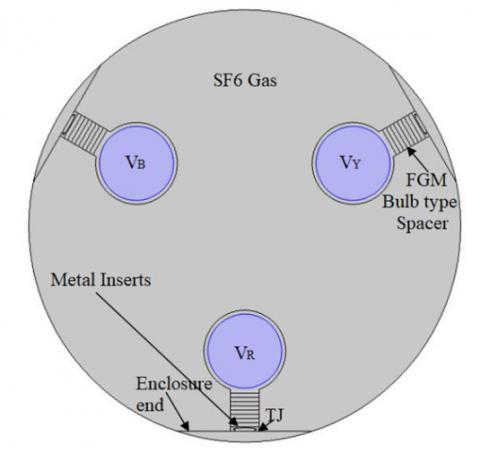
Regardless of the environment, the power system network must be continuously operational. Current spacer failures of Gas Insulated Busduct (GIB) have been noted as a result of a number of manufacturing and switching faults, including delamination, protrusion, depression, gap, etc. These defects have a severe negative effect on the insulator's surface, which de-energises the gas-insulated busduct device and causes a significant financial loss. For the purpose of studying the electric stress at the Triple Junction, a Functionally Graded Material (FGM) spacer is built for a three phase GIB with protrusion irregularity in this work. The stress is reduced by inserting metal inserts at the end of the zero potential. Functionally graded materials are spatially distributed with numerous filler materials to achieve homogeneous electric field stress by doping them with various permittivity values. The spacer used in the simulation is made to withstand a range of voltages as well as varied FGM gradings. Grading's impact on electric field stress is identified and further diminished with the addition of the MI to the FGM insulator. The outcomes are discussed and analysed to demonstrate how well the proposed spacer works.
FGM, electric field stress, insulator, triple junction, metal insert, gas insulated busduct
Only fossil fuels like gasoline and natural gas are used to generate the vast majority of the world's power, which poses a huge risk to both the economy and ecological of the planet. Electrochemical energy production is one of the alternative energy sources that has received much study. But first, sustainability and environmentally friendly production must be met. Humankind requires safe and reliable power that is environmentally friendly and economic. In this context, Gas Insulated Substations have proven to be the right alternative to the humankind needs. In the present days, the sustained supply of electricity requires that substations be operational at all times. The existing air-insulated substations are failing to do so due to their frequent shutdowns which are owing to the loss of energy. To overcome this demerit of the existing substations, the gas insulated substations conceptually plays a vital role as the entire transmission system is enclosed in a chamber that is filled with dielectric gas to prevent loss of energy and also to provide a continuous and reliable power. Electric substations may sustain severe damage as a result of human-caused physical assaults and criminal activity. Many utilities are investigating design solutions to lessen the consequences of criminal activity directed at substations in addition to limiting potential damage to substations from natural disasters as a result of criminal attacks on crucial substations. Currently, urbanization and energy consumption are both expanding swiftly, and the GIB is gaining popularity. Gas-insulated switchgear-using substations must meet these issues while maximizing their return on investment. This calls for reducing overall costs, boosting dependability, preserving operational flexibility, and controlling the impact of their operations on the environment.
Numerous studies on spacers have been published in the literature, and it has been stated that the GIB spacers' embedded defects are what cause the insulation to deteriorate over time. Li D [1] put up a surface potential measurement platform of the simplified post spacer based on the active electrostatic probe method and researched the characteristics of surface charge accumulation on spacer in gas-insulated gearbox line (GIL) under AC voltage. Yao Y. [2] modified the structure form of the insulating spacer using the approach of uneven rational B-spline curve fitting. An intelligent optimisation technique is used to optimise the geometry of the centre connector, high voltage shield, and insulating spacer. The maximum electric field near the gas area of the insulating spacer is reduced when the shape before and after optimization are compared.
In a miniaturized de gas insulated gearbox line (GIL), Li J. [3] used models and tests to examine the mechanisms of surface charging and surface modification of epoxy spacer that affect the lifting voltage and the motion trajectory of spherical metal particles. Based on actual measured conductivity characteristics of SiC-filled epoxy composites and permittivity characteristics of $\mathrm{SrTiO3}$-filled epoxy composites, Rachmawati [4] studied the electric field reduction impact provided by permittivity and conductivity graded materials.
An axisymmetric electrode-spacer design utilised in a Gas Insulated Substation (GIS), typically for $12-420 \mathrm{kV}$ operations, was optimised by Dasgupta S. [5] for the distribution of $\mathrm{E}_{\text {stress }}$ over the live electrode. Constrained linear programming problems (LPPs) are solved using the Simplex Algorithm, which is the foundation of the technology.
Wang C. [6] used the finite element approach and a numerical optimisation method to create a compact design for a $550 \mathrm{kV}$ basin-type spacer. The surface electric field of the spacer is evenly distributed, and localised concentrated mechanical stresses at the central conductor or sealed tank are significantly reduced under the condition of a $10 \%$ reduction in insulation distance between the central conductor and sealed tank. Yao H. [7] developed a brand-new idea for an SFGM spacer to control the dispersion of the electric field. The electric field distribution was examined, and the impact of the non-uniform electric field on the motion behaviours of particles was analysed, using a simplified model of the S-GIL with various epoxy spacers.
In few research [8-17] have examined the effects of various anomalies and evaluated insulators like post type, cone type, etc. but so for bulb type spacer is a new model of spacer for three phase GIB. The investigation of $\mathrm{E}_{\text {stress }}$ in GIB has been the work of numerous authors. Numerous studies have used techniques other than shape control, including FGM with different grades, to study the electric field stress $\left(\mathrm{E}_{\text {stress }}\right)$ at the TJs, of the spacer, due to the limitations of single-phase GIS. Functionally graded materials (FGMs) are potential prospects for the manufacture of technological parts, including structural devices like solid oxide fuel cells (SOFC) and high-efficiency hybrid direct energy conversion systems as well as electrochemical ones like SOFC. Spatial distribution of permittivity is used in the FGM spacer to control the electric field distribution in and around the spacer. The electric field calculations for several types of FGM spacers may be performed using the Finite Element Method (FEM).
Numerous writers have contributed to the study of $\mathrm{E}_{\text {stress }}$ in GIB, while few studies have looked at the effects of different anomalies as well as insulators of the cone, disc, and other types but not the bulb type. Whereas by considering dielectric failures of insulators as a challenge in a three-phase GIB the literature has been carried out on the several defects like Delamination and void on the solid materials. Metal protrusions is usually initiated on the convex and curved sides of spacers and are formed mostly by means of scratches upon the surface of the spacer as a result of poor care during assembly, switching activities, and lightning shocks. At high voltage, the form of the protrusion tips can be sharp or spherical. These defects can influence the electric stress distribution over the spacer length. Analysis has to be carried out for different radii of protrusions at different locations along the spacer surface.
The effect of $\mathrm{E}_{\text {stress }}$ on a three-phase GIB under a spacer of the FGM bulb type is investigated in this paper. In order to reduce $\mathrm{E}_{\text {stress }}$ at TJs and maintain a consistent field along its surface, MI are placed at the zero potential end. The metal component that was recessed successfully insulated the triple connection, lowering the $\mathrm{E}_{\text {stress }}$ at TJ. This MI strategy lessened the expense and inconvenience of replacing the insulator. A three-phase GIB simulation is performed once the conductors are correctly assigned to charge conservation. Following the computation of the intended model, the features for $\mathrm{E}_{\text {stress }}$ at the high potential end close to the TJ of the FGM spacer were assessed, the factors that govern the distribution of $\mathrm{E}_{\text {stress }}$.
Researchers have calculated the $\mathrm{E}_{\text {stress }}$ using the boundary conditions of the Laplace and Poisson equations. These equations are used to calculate ' $\mathrm{E}_{\text {stress }}$ ', since it is regarded to be difficult to calculate it analytically. Despite the presence of several numerical approaches, the finite element method (FEM) is used to solve complex problems. According to Eq. (1), the electric flux density $(\vec{D})$ can be represented in terms of the $\mathrm{E}_{\text {stress }}(\vec{E})$.
$\vec{D}=\varepsilon \vec{E}$ (1)
The electric flux density $\vec{D}$ with $\mathrm{Q}_{\mathrm{i}}$ as electrical charge can be written in a closed surface as Eq. (2).
$\oint_S \vec{D} \bullet \overrightarrow{d S}=Q_i$ (2)
where,$\vec{E}$ is given by Eq. (3)
$\vec{E}=-\left(\overrightarrow{a_x} \frac{\partial}{\partial x}+\overrightarrow{a_y} \frac{\partial}{\partial y}+\overrightarrow{a_z} \frac{\partial}{\partial z}\right) V$ (3)
Eq. (4) provides the overall $\mathrm{E}_{\text {stress }}$ in its $x$ and $y$ coordinates.
$\vec{E}=\overrightarrow{a_x} \frac{\partial V(x, y)}{\partial x}-\overrightarrow{a_y} \frac{\partial V(x, y)}{\partial y}$ (4)
According to divergence theorem,
$\left(\overrightarrow{a_x} \frac{\partial}{\partial x}+\overrightarrow{a_y} \frac{\partial}{\partial y}+\overrightarrow{a_z} \frac{\partial}{\partial z}\right) \cdot\left(\overrightarrow{a_x} \frac{\partial D_x}{\partial x}+\overrightarrow{a_y} \frac{\partial D_y}{\partial y}+\overrightarrow{a_z} \frac{\partial D_z}{\partial z}\right)=\rho_v$ (5)
from Eq. (2), Eq. (3) and Eq. (5),
$\left(\overrightarrow{a_x} \frac{\partial}{\partial x}+\overrightarrow{a_y} \frac{\partial}{\partial y}+\overrightarrow{a_z} \frac{\partial}{\partial z}\right) \cdot \varepsilon\left(\overrightarrow{a_x} \frac{\partial E_x}{\partial x}+\overrightarrow{a_y} \frac{\partial E_y}{\partial y}+\overrightarrow{a_z} \frac{\partial E_z}{\partial z}\right)=\rho_v$ (6)
$\left(\overrightarrow{a_x} \frac{\partial}{\partial x}+\overrightarrow{a_y} \frac{\partial}{\partial y}+\overrightarrow{a_z} \frac{\partial}{\partial z}\right) \cdot \varepsilon\left(-\left(\overrightarrow{a_x} \frac{\partial}{\partial x}+\overrightarrow{a_y} \frac{\partial}{\partial y}+\overrightarrow{a_z} \frac{\partial}{\partial z}\right) V\right)=\rho_v$ (7)
When the dielectric materials are homogeneous, linear, and isotropic, Eq. (9) can be simplified to Eq. (10).
$\Gamma V=\frac{-\rho_v}{\varepsilon} \quad$ Where $\quad \Gamma=\frac{\partial^2}{\partial x^2}+\frac{\partial^2}{\partial y^2}+\frac{\partial^2}{\partial z^2}$ (8)
Volume charge density is reduced when there is uniform charge distribution, and Eq. (8) above is simplified to Eq. (9).
$\Gamma V=0$ (9)
Figure 1. Bulb type spacer
The typical representation of a bulb shaped spacer is shown in Figure 1. In particular, the surfaces of the spacer are assumed to be devoid of any surface charges, therefore the typical components of the flux densities on either side of the epoxy spacer/SF6 gas contact are supposed to be constant.
The amount of electrical energy stored $W$ in the full volume ' $v$ ' of the region under consideration is given by
$W=\frac{1}{2} \iiint \varepsilon\left(\nabla^2 V\right) d v$ (12)
Eq. (13), which includes the potential's $\mathrm{x}$ and $\mathrm{y}$ components, provides ' $W$ ', total stored energy in this corresponding area.
$W=\frac{1}{2} \iiint\left(\varepsilon_x \frac{\partial^2 V}{\partial x^2}+\varepsilon_y \frac{\partial^2 V}{\partial y^2}\right) d x d y d z$ (13)
It is reduced even further to
$\frac{W}{z}=\frac{1}{2} \iint\left(\varepsilon_x \frac{\partial^2 V}{\partial x^2}+\varepsilon_y \frac{\partial^2 V}{\partial y^2}\right) d x d y$ (14)
where , W/z is energy density in small area dxdy
$d W=\frac{1}{2} \iint\left(\varepsilon_x \frac{\partial^2 V}{\partial x^2}+\varepsilon_y \frac{\partial^2 V}{\partial y^2}\right) d x d y$ (15)
then,
$d W=\frac{1}{2} \iint \varepsilon\left(\nabla^2 V\right) d x d y=0$ (16)
As $\nabla^2 V=0$, from Eq. (11) and Eq. (16),
$d W=0$ (17)
To address this shortcoming of traditional composites, a new class of composites known as functionally graded materials was developed. High strength and toughness functionally graded materials (FGM) are able to retain a lengthy operating life while being subjected to such a large temperature difference under the influence of mechanical load and temperature gradient produced thermal stress. When utilising centrifugal casting, the mould is spun while gravity is used to create the functionally graded material. A spinning mould is used to cast metal from molten form, and the process is repeated until the metal solidifies. This is a common way for creating cylindrical components. It is possible that the mechanical qualities of the casting will improve by 10-15% if this technique is used to raise the metal density. Because of the density differential between molten and solid particles, centrifugal force generates a compositional gradient in FGM as shown in Figure 2. Gradients have constraints since they are the result of naturally occurring processes (such as centrifugal force and density difference), as was discovered through a survey of the relevant literature.
Despite the fact that there are a number of ways available, this study uses the permittivity variation approach with three alternative grading schemes, including Low Graded type FGM (LG-FGM), High Graded Type FGM (HG-FGM) and U Shaped Graded Type FGM (UG-FGM), to create a Bulb spacer for the three phase GIB that has a con sistent field distribution over its length. Here, the complete length of the Bulb type spacer is divided into 10 equal gradings, resulting in three separate permittivity ranges for the various types of FGM grading. Following is a detailed description of the three gradings.
1. Low Graded type functionally graded material (LGFGM)
Centrifugal forces are applied to an epoxy mixture comprising titanium oxide $\left(\mathrm{TiO}_2\right)$ and aluminium oxide $\left(\mathrm{Al}_2 \mathrm{O}_3\right)$ as part of the LG-FGM grading technique. Permittivity being a function of radius, it is important to retain the high permittivity at the end of the inner conductor while gradually reducing the radius in the direction of the end of the zero potential. In case 1 , the conductor's permittivity to the enclosure ranges between 3.95 and 3.5, in case 2, 4.05 to 3.6, and in case 3, 4.15 to 3.7.
2. High Graded type functionally graded material (HGFGM)
Low permittivity at the high potential end and high permittivity at the zero potential end and an increase in permittivity that gradually moves towards the zero potential end, the same process is used for high graded FGM. In cases 1, 2, and 3, respectively, the permittivity is between 3.5 and 3.95 from the conductor to the enclosure, 3.6 and 4.05, and 3.7 and 4.15.
3. U Shaped Graded Type functionally graded material (UG-FGM)
U Graded Type functionally graded material, where the concentration of filler with high permittivity, or 3.95 at the high potential end, is gradually decreased to 3.5, then gradually increased to 3.95 nearer the zero potential end. Similar changes are made to instances 2 and 3, where the permittivity is modified from 4.05 to 3.6 to 4.05 and from 4.15 to 3.7 to 4.15, respectively.
Figure 2. Designed FGM bulb type spacer
The bulb type spacer is intended for use with a three-phase GIB that contains SF6 gas with a relative permittivity of 1.0015. The HV and LV wires are encased inside the zero potential end. Figure 3 depicts the three-phase GIB simulation utilising FEM analysis and a composite with epoxy-alumina as the insulator material.
Figure 3. Three phase GIB design model
The design schematics for the FGM bulb type spacer without and with MI, respectively, are shown in Figures 4 and 5. The 10 equal grades that are the same height as the insulator's length and width make up the FGM insulator's design. In the three various forms of FGM technique that are being evaluated, the grading is carried out using separate permittivity ranges; the ranges are chosen to be 3.5 to 3.95, 3.6 to 4.05 , and 3.7 to 4.15 in instances 1, 2, and 3, respectively. The FGM spacer is also examined for these three grading types. In the aforementioned situations, grading Low, High, and U-FGM with the respective permittivity ranges. A MI at the high potential end and zero potential end of the FGM bulb type spacer can also help to lower the $\mathrm{E}_{\text {stress. }}$
Figure 4. FGM bulb type spacer without MI
Figure 5. FGM bulb type spacer with MI
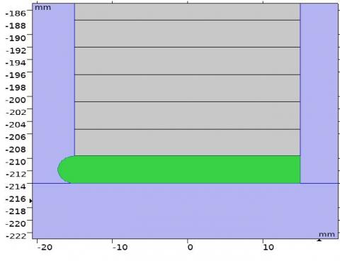
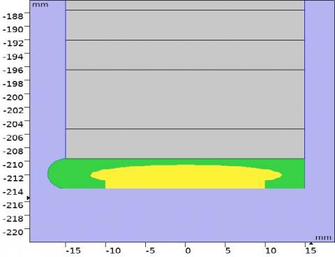
The three phase GIB with protrusion defect for bulb spacers without and with MI, respectively, is shown in Figures 6 and 7. An appropriate MI with rectangular dimensions of 12 mm width and 1 mm height was constructed in order to lessen this effect, and an ellipse with a-axis of 9.4 mm and b-axis of 1 mm was found to have the maximum reduction of $\mathrm{E}_{\text {stress. }}$. This MI was consequently developed for both the high potential and zero potential end. Additionally, by adding a MIto both ends of the FGM bulb type spacer, the $\mathrm{E}_{\text {stress }}$ of the spacer may be reduced. Figure 7 depicts the suggested MI with the specified dimensions.
Figure 6. Design of bulb type spacer with protrusion
Figure 7. Design of bulb type spacer with protrusion and MI
When compared to the previous cases, Table I shows that LG-FGM Grading in case 3 has a significant $\mathrm{E}_{\text {stress }}$ at the TJs of the zero potential end and high potential ends over applied voltages of V1, V2, V3. Table II demonstrates that LG- FGM Grading has the least decrease in $\mathrm{E}_{\text {stress }}$ at the TJ's of the zero potential end and high potential ends when compared to $\mathrm{HG}$ and UG- FGM Grading for all situations throughout applied voltages of V1, V2, and V3. The Estress derived in Tables I and II is compared, and the percentage reduction is determined for all the cases and it is noticed that for $\mathrm{HG}$ case 2 on conductor $B$ has maximum reduction for all the operating voltages.
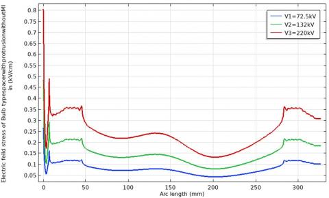
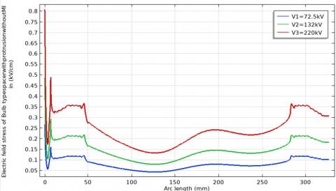
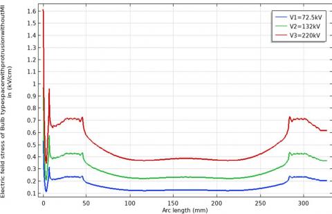
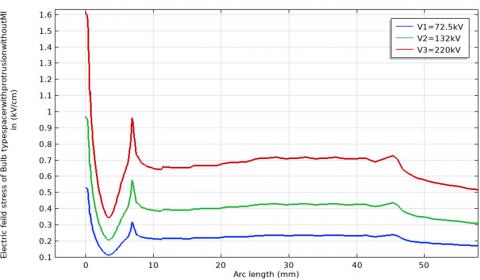
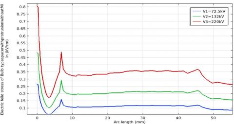
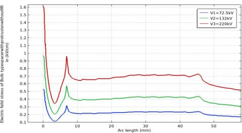
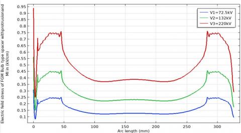
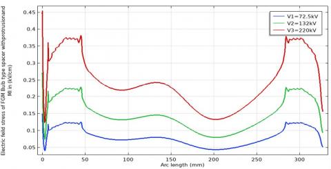
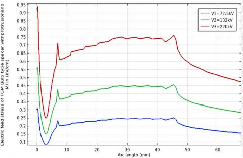
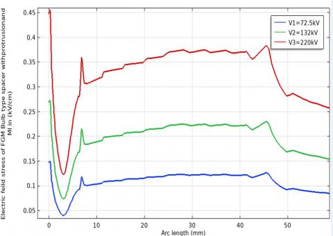
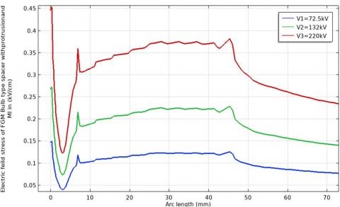
As demonstrated in Figures 8 to 10 the value of $E_{\text {stress }}$ at the zero potential end, i.e. at zero arc length, is greater than that at the high potential end. In the magnified version, as shown in Figures 11 to 13 the value of the $\mathrm{E}_{\text {stress }}$ is clearly visible. The $\mathrm{E}_{\text {stress }}$ at the zero potential end owing to protrusion is minimised by utilising MI at the TJs, as shown in Figures 14 to 19.
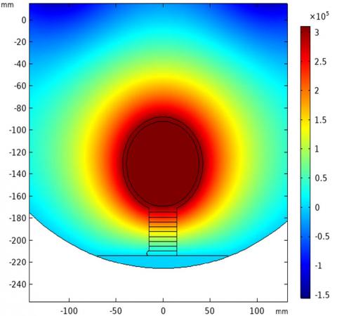
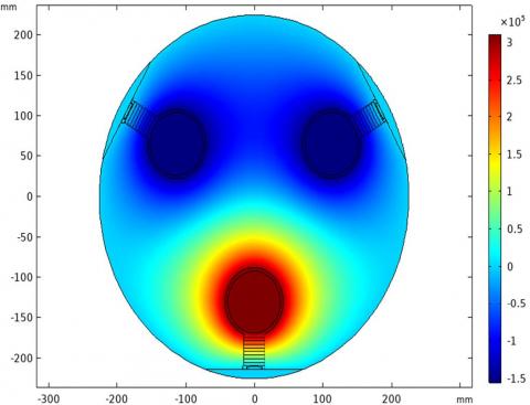
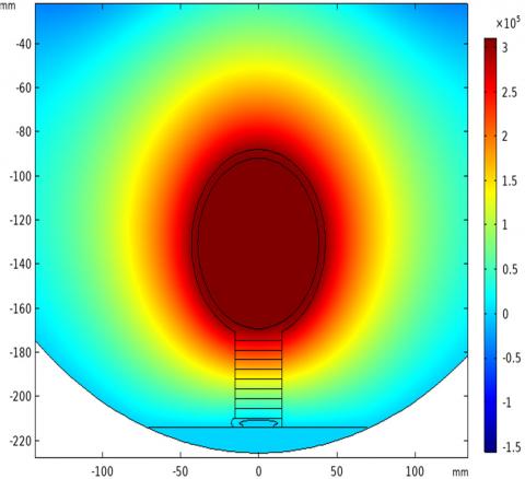
The surface plots of the designed bulb type spacer are shown in Figures 20 to 23. Due to its high potential, the red colour represents high electric stress at the high potential end, whereas the dark blue colour indicates high electric stress at the zero potential end ends. When compared to the high potential end, the thick red lines demonstrate significant electric stress at TJ of the zero potential end end due to protrusion. Inserting MI, reduces the high stress even further.
Figure 8. Estress plot of conductor R of a bulb type spacer
Figure 9. Estress plot of conductor Y
Figure 10. Estress plot of conductor B
Figure 11. Zoom plot of Estress plot of conductor R
Figure 12. Zoom plot of Estress plot of conductor R
Figure 13. Zoom plot of Estress plot of conductor R
Figure 14. Estress plot of conductor R with MI
Figure 15. Estress plot of conductor Y with MI
Figure 16. Estress plot of conductor B with MI
Figure 17. Zoom plot of Estress plot of conductor R with MI
Figure 18. Zoom plot of Estress plot of conductor Y with MI
Figure 19. Zoom plot of Estress plot of conductor B with MI
Figure 20. Surface plot without MI
Figure 21. Zoomed surface plot without MI
Figure 22. Surface plot with MI
Figure 23. Zoomed surface plot with MI
Table 1. Protrusion effect for FGM bulb type spacer
|
Grading |
Conductor |
Permitivity Values |
V1=72.5kV |
V2=132kV |
V3=220kV |
|||
|
Estress at Zero Potential End in KV/cm |
Estress at High Potential in KV/cm |
Estress at Zero Potential End in KV/cm |
Estress at High Potential in KV/cm |
Estress at Zero Potential End in KV/cm |
Estress at High Potential in KV/cm |
|||
|
LG-FGM |
R |
I Case |
0.5002 |
0.1295 |
0.9107 |
0.2357 |
1.5179 |
0.3932 |
|
II Case |
0.5123 |
0.1285 |
0.9327 |
0.2339 |
1.5544 |
0.3898 |
||
|
III Case |
0.5423 |
0.1283 |
0.9546 |
0.2338 |
1.591 |
0.3894 |
||
|
Y |
I Case |
0.2506 |
0.0807 |
0.4563 |
0.1473 |
0.7605 |
0.2454 |
|
|
II Case |
0.2567 |
0.0791 |
0.4673 |
0.1463 |
0.7788 |
0.2438 |
||
|
III Case |
0.2627 |
0.08 |
0.4783 |
0.1457 |
0.7972 |
0.2433 |
||
|
B |
I Case |
0.25 |
0.0807 |
0.4552 |
0.1469 |
0.7587 |
0.2449 |
|
|
II Case |
0.256 |
0.0804 |
0.4662 |
0.1463 |
0.7769 |
0.2439 |
||
|
III Case |
0.2621 |
0.08 |
0.4771 |
0.1457 |
0.7952 |
0.2428 |
||
|
HG-FGM |
R |
I Case |
0.5024 |
0.132 |
0.9148 |
0.2413 |
1.5246 |
0.2404 |
|
II Case |
0.5145 |
0.1313 |
0.9367 |
0.24 |
1.5611 |
0.3998 |
||
|
III Case |
0.5625 |
0.1311 |
0.9586 |
0.2378 |
1.5977 |
0.3977 |
||
|
Y |
I Case |
0.2518 |
0.1505 |
0.4584 |
0.1505 |
0.764 |
0.2509 |
|
|
II Case |
0.2578 |
0.0822 |
0.4694 |
0.1497 |
0.7823 |
0.2496 |
||
|
III Case |
0.2638 |
0.078 |
0.4803 |
0.1486 |
0.8006 |
0.2483 |
||
|
B |
I Case |
0.2511 |
0.0825 |
0.4572 |
0.1502 |
0.762 |
0.2503 |
|
|
II Case |
0.2571 |
0.0808 |
0.4681 |
0.1494 |
0.7802 |
0.249 |
||
|
III Case |
0.2631 |
0.0816 |
0.4671 |
0.1487 |
0.7895 |
0.2478 |
||
|
UG-FGM |
R |
I Case |
0.5079 |
0.1296 |
0.9427 |
0.2341 |
1.5411 |
0.3929 |
|
II Case |
0.5199 |
0.129 |
0.9466 |
0.2348 |
1.5776 |
0.3914 |
||
|
III Case |
0.5319 |
0.1283 |
0.9685 |
0.2329 |
1.6141 |
0.3984 |
||
|
Y |
I Case |
0.2545 |
0.0807 |
0.4634 |
0.1473 |
0.7723 |
0.2455 |
|
|
II Case |
0.2605 |
0.0805 |
0.4743 |
0.1466 |
0.7905 |
0.2444 |
||
|
III Case |
0.2665 |
0.08 |
0.4853 |
0.1457 |
0.8088 |
0.2434 |
||
|
B |
I Case |
0.2538 |
0.0809 |
0.4621 |
0.808 |
0.7702 |
0.2454 |
|
|
II Case |
0.2598 |
0.0805 |
0.4731 |
0.1466 |
0.7885 |
0.2444 |
||
|
III Case |
0.2658 |
0.0802 |
0.484 |
0.1457 |
0.8607 |
0.2433 |
||
Table 2. Reduction of Estress for FGM bulb type spacer with MI
|
Grading |
Conductor |
Permitivity Values |
V1=72.5kV |
V2=132kV |
V3=220kV |
|||
|
Estress at Zero Potential End in KV/cm |
Estress at High Potential in KV/cm |
Estress at Zero Potential End in KV/cm |
Estress at High Potential in KV/cm |
Estress at zero Potential End in KV/cm |
Estress at High Potential in KV/cm |
|||
|
LG-FGM |
R |
I Case |
0.2897 |
0.1295 |
0.5274 |
0.2357 |
0.897 |
0.3928 |
|
II Case |
0.2958 |
0.1298 |
0.5386 |
0.2326 |
0.8977 |
0.3877 |
||
|
III Case |
0.302 |
0.1283 |
0.5498 |
0.2338 |
0.9164 |
0.3894 |
||
|
Y |
I Case |
0.1405 |
0.0807 |
0.2559 |
0.1473 |
0.4264 |
0.2455 |
|
|
II Case |
0.1435 |
0.0805 |
0.2613 |
0.1466 |
0.4355 |
0.2443 |
||
|
III Case |
0.1465 |
0.0802 |
0.2667 |
0.1457 |
0.4445 |
0.2434 |
||
|
B |
I Case |
0.145 |
0.0807 |
0.2549 |
0.1469 |
0.4249 |
0.2454 |
|
|
II Case |
0.143 |
0.0791 |
0.2604 |
0.1463 |
0.4339 |
0.2438 |
||
|
III Case |
0.146 |
0.0801 |
0.2658 |
0.146 |
0.443 |
0.2433 |
||
|
HG-FGM |
R |
I Case |
0.2957 |
0.1325 |
0.5384 |
0.2413 |
0.8973 |
0.402 |
|
II Case |
0.3012 |
0.1317 |
0.5484 |
0.241 |
0.914 |
0.3998 |
||
|
III Case |
0.3067 |
0.1311 |
0.5583 |
0.2387 |
0.9306 |
0.3979 |
||
|
Y |
I Case |
0.1435 |
0.0825 |
0.2613 |
0.1506 |
0.4355 |
0.2503 |
|
|
II Case |
0.1461 |
0.0821 |
0.2661 |
0.1497 |
0.4435 |
0.2496 |
||
|
III Case |
0.1488 |
0.0816 |
0.2708 |
0.149 |
0.4514 |
0.2483 |
||
|
B |
I Case |
0.143 |
0.0827 |
0.2604 |
0.1506 |
0.434 |
0.2509 |
|
|
II Case |
0.1456 |
0.0822 |
0.2652 |
0.1497 |
0.442 |
0.249 |
||
|
III Case |
0.1483 |
0.0803 |
0.27 |
0.1486 |
0.4499 |
0.2483 |
||
|
UG-FGM |
R |
I Case |
0.2988 |
0.1276 |
0.544 |
0.2357 |
0.9067 |
0.3929 |
|
II Case |
0.3043 |
0.1278 |
0.554 |
0.2347 |
0.9233 |
0.3914 |
||
|
III Case |
0.3097 |
0.1281 |
0.5639 |
0.2337 |
0.9398 |
0.3894 |
||
|
Y |
I Case |
0.145 |
0.0807 |
0.264 |
0.1473 |
0.44 |
0.2449 |
|
|
II Case |
0.1476 |
0.0804 |
0.2688 |
0.1463 |
0.448 |
0.2444 |
||
|
III Case |
0.1502 |
0.0802 |
0.2735 |
0.146 |
0.4559 |
0.2434 |
||
|
B |
I Case |
0.1445 |
0.0809 |
0.2631 |
0.1472 |
0.4385 |
0.2454 |
|
|
II Case |
0.1471 |
0.0805 |
0.2679 |
0.1463 |
0.4465 |
0.2444 |
||
|
III Case |
0.1497 |
0.0802 |
0.2726 |
0.146 |
0.4544 |
0.2434 |
||
In this article, the impact of protrusion on a three-phase GIB is examined. The impact is lessened by inserting a MI at the enclosing end of the insulator, TJ. For the bulb type spacer at various operating voltages at TJ's, the maximum electric stress is achieved at the zero potential end as opposed to the high potential end for protrusion defect.It was revealed that case 3 exhibited significant electric stress at the TJ's of the zero potential end and high potential ends across all applied voltages when LG-FGM grading was compared to other instances for fault protrusion.
The greatest percentage reduction in electric stress is experienced at the TJ of the zero potential end in all situations of LG, HG, and UG-FGM gradings. The acquired $\mathrm{E}_{\text {stress }}$ due to protrusion has been decreased by inserting a recessed MI at the TJ of the zero potential end and high potential end.
[1] Li D., Zhang G., Wang T., “Characteristics of Surface Charge Accumulation on Truncated Cone-type Insulator Under AC Voltage”, (2022) Gaodianya Jishu/High Voltage Engineering, 48 (4), pp. 1480 - 1488, DOI: 10.13336/j.1003-6520.hve.20210017
[2] Yao Y., Wang Z., Chen S., Lin X., Cui Z., Zhang H., Geng Z., “Optimization Design on Insulating Spacer and Its Assembly Structure of 550 kV GIL “, (2021) GaoyaDianqi/High Voltage Apparatus, 57 (5), pp. 50 - 57, DOI: 10.13296/j.1001-1609.hva.2021.05.008
[3] Li J., Wang Y., Dong J., Liang H., Du B., Xu Y., Li X., “Surface Charging Affecting Metal Particle Lifting Behaviors Around Epoxy Spacer of HVDC GIL/GIS”, (2022) IEEE Transactions on Dielectrics and Electrical Insulation, 29 (4), pp. 1546 – 1552. DOI: 10.1109/TDEI.2022.3183673
[4] Rachmawati, Kojima H., Kato K., Zebouchi N., Hayakawa N., “Electric Field Grading and Discharge Inception Voltage Improvement on HVDC GIS/GIL Spacer with Permittivity and Conductivity Graded Materials (ϵ/σ-FGM) “, (2022) IEEE Transactions on Dielectrics and Electrical Insulation, 29 (5), pp. 1811 - 1817, DOI: 10.1109/TDEI.2022.3194489
[5] Dasgupta S., Baral A., Lahiri A., “Optimization of Electrode-Spacer Arrangement Using Simplex Algorithm “, (2023) IEEE Transactions on Dielectrics and Electrical Insulation, 30 (2), pp. 726 - 733, DOI: 10.1109/TDEI.2023.3242628
[6] Wang C., Li W., Chen T., Li W., Gong R., Zhang G. “Compact Design of 550 kV Basin-Type Spacer in Gas Insulated Switchgear (Part I) -- Structure Optimization”, (2022) DiangongJishuXuebao/Transactions of China Electrotechnical Society, 37 (7), pp. 1847 – 1855, DOI: 10.19595/j.cnki.1000-6753.tces.210539
[7] Yao H., Du B.X., Li J., Wang Y.H., Liang H.C., Dong J.N., Zhang C., He J., Chen R., “Motion Behaviours of Metal Particle around SFGM Spacer under Non-uniform Electric Field”, (2020) 2020 IEEE International Conference on Applied Superconductivity and Electromagnetic Devices, ASEMD 2020, art. no. 9276282, DOI: 10.1109/ASEMD49065.2020.9276282
[8] Xing Y., Sun X., Jiang J., Liang F., Liang Z., Zhuang W., Liu B., Li D., Cao S., Li M., He J., Li C., “Significantly suppressing metal particle-induced surface charge accumulation of spacers in DC gas-insulated power transmission lines”, (2022) Journal of Physics D: Applied Physics, 55 (50), art. no. 504003, DOI: 10.1088/1361-6463/ac9ce6
[9] Li J., Wang Y., Chen Y., Liang H., Du B., Zhu W., “Design and Optimization of 1000 kV DC GIL Post Spacer with Surface Conductivity Gradient for ITER Neutral Beam Injector”, (2020) 2020 IEEE International Conference on Applied Superconductivity and Electromagnetic Devices, ASEMD 2020, art. no. 9276342.DOI: 10.1109/ASEMD49065.2020.9276342
[10] Wang Y., Li J., Xiao M., Liang H., Yao H., Du B.,” The Improvement of Flashover Characteristics with Field Grading CCTO Coating for GIL Spacer”, (2021) ICEMPE 2021 - 3rd International Conference on Electrical Materials and Power Equipment, art. no. 9509078, DOI: 10.1109/ICEMPE51623.2021.9509078
[11] Hayakawa N., Kato K., Hikita M., Okubo H., Watanabe K., Adachi K., Okamoto K., “Development of Cone- Type FGM Spacer for Actual Size GIS “, (2020) Annual Report - Conference on Electrical Insulation and Dielectric Phenomena, CEIDP, 2020-October, art. no. 9437434, pp. 255 - 258.DOI: 10.1109/CEIDP49254.2020.9437434
[12] Kim M.-S., Hong D.-S., Cho Y.-S., Yun C.-G., Cho H.- G., “A Study on the Accelerated Life Models for Lifetime Prediction of the GIS based on Insulation Spacer “, (2022) ICEPE-ST 2022 - 2022 6th International Conference on Electric Power Equipment - Switching Technology, pp. 241 - 244.DOI: 10.1109/ICEPE- ST51904.2022.9757106
[13] Inoue Y., Kozako M., Hikita M., Masui H., Yanase H., Okamoto K., “Effects of Nano-micro-Composite and Shielding on Flashover Characteristics of Gas Insulated Switchgear Spacer Model in Different Lightning Impulse Application Methods”, (2021) Annual Report - Conference on Electrical Insulation and Dielectric Phenomena, CEIDP, 2021-December, pp. 399 - 402, DOI: 10.1109/CEIDP50766.2021.9705320
[14] Liang H., Du B., Kong X.X., “Basin-Type Spacer for DC-GIL-Part II: Surface Charge and Electric Field Regulation”, (2022) IEEE Transactions on Dielectrics and Electrical Insulation, 29 (3), pp. 1119 - 1126, DOI: 10.1109/TDEI.2022.3168342
[15] Zhao C., Tang Z., Zhang L., Wu D., Xia H., Li H., Pan K., “Entire process of surface discharge of GIS disc- spacers under constant AC voltage “, (2020) High Voltage, 5 (5), pp. 591 - 597, DOI: 10.1049/hve.2019.0140
[16] Zebouchi N., Haddad M.A., “A review on real-size epoxy cast resin insulators for compact high voltage direct current gas insulated switchgears (Gis) and gas insulated transmission lines (gil)-current achievements and envisaged research and development”, (2020) Energies, 13 (23), art. no. 6416, DOI: 10.3390/en13236416
[17] Fabio M.R., Hidayat S., Khayam U., “Effects of Notches in GIS Spacer Design to Hold Conductor Rods on Electric Field Distribution”, (2021) 2021 3rd International Conference on High Voltage Engineering and Power Systems, ICHVEPS 2021, pp. 241 - 246. DOI: 10.1109/ICHVEPS53178.2021.9601002