Aakriti Pandey* | Swapnajit Pattnaik
© 2022 IIETA. This article is published by IIETA and is licensed under the CC BY 4.0 license (http://creativecommons.org/licenses/by/4.0/).
OPEN ACCESS
The typical voltage of fuel cells is low for efficient utilisation and thus, a high-boost DC-DC converter is required to uplift the voltage. In this article, a novel DC-DC converter for fuel cell application is proposed that uses the technique of bifurcating the duty ratio such that a single switch is not subjected to an extreme duty ratio. With this technique, the inductors are first charged in parallel mode followed by charging in series mode which yields high gain ratio at comparatively lesser duty ratio of the switches. The switched capacitor is also used in combination to further uplift the gain. The major advantage of this converter is the broad range of gain obtained from combination of duty ratios. The modes of operation in continuous and discontinuous condition, design consideration, stress on the semiconductor devices is described explicitly. Also, the effect of internal resistances on the gain and the efficiency investigation of the converter is presented. The merits of the designed converter are justified by comparison with other topologies. The verification of the theoretical analysis done by experimental setup of 150W prototype.
Fuel Cell, High-boost DCDC Converter, Renewable Energy, Fuel Cell Powered Electric Vehicle
With the fast depletion of fossil fuels and the drastic increment in the greenhouse gas emission, fuel cell powered vehicle (FCPEV) has emerged to be the best possible common solution. The FCEVs are clean alternative to conventional energy resources and their prime advantage is the zero emission which is the most crucial demand in today's times with increaing greenhouse gases and their alarming adverse effects like global warming.
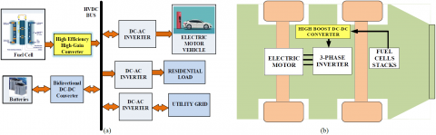
In the fuel cells, electrical energy is generated by electrochemical reactions using three vital parts, namely cathode, anode and electrolyte [1]. It utilizes hydrogen and oxygen to generate heat, water and electricity forming an indispensable, clean, reliable, noise-less, emission-free and efficient form of energy. The energy produced by fuel cell can be connected to the local loads or to the utility grid as shown in Figure1(a). The FCPEVs are one of the most efficient and highly advantageous application of the fuel cells but the major concern in utilisation of fuel cell is the low terminal outpult voltage, high current and inverse output characteristic which increases the output current with decline in output voltage [2]. Thus, a high-boost converter is required for interfacing the fuel cell and DC link inverter as depicted in Figure1(b). The high-boost converter should have widespread range of gain ratio to work along the inverse output characteristic of the fuel cell.
The basic traditional boost converter cannot be used for such applications owing to the extreme duty ratio needed for high voltage gain. It can lead to serious diode reverse recovery problem, high voltage stress on the switch and increase in conduction losses. Moreover, the electromagnetic interference (EMI) and the higher rating of components and switches required also make it unfeasible [6]. Thus, specifically designed high-gain converters are required for this purpose. There are several types of step-up dc-dc converter topologies proposed in literature. The high gain DC-DC converter can be broadly classified in two categories: Isolated and Non-Isolated Converters.
The push-pull, half and full bridge, flyback converter, etc. are some of the types of isolated high-gain converters [7, 8] in which the turn ratio of the transformer is used to impart the desired gain ratio. Nevertheless, due to the leakage inductance of the transformer, there is a higher power dissipation and voltage spike in the switches. To manage this, there is requirement of additional active clamping and snubber circuit which increases the cost and complexity of the converter [9]. Apart from this, transformer core saturation is also one of the major concerns in such type of converters.
The non-isolated high gain DC-DC converters are an economical choice when galvanic isolation is not required. In these converters, various techniques have been proposed in literature for the achievement of the high gain ratio without use of extreme duty cycle. In [10], coupled inductor is utilized to achieved the high gain. Here, the energy stored in the magnetizing inductance is utilized and voltage is uplifted with the help of turn-ratio of the coupled inductor. The limitation of this technique is the increased time for transient response due to the larger inductance of the coupled inductor [11]. In [13,14], switched capacitors technique is used for providing higher gain but the high current and the switch voltage stress impose a serious limitation. Another technique of non-isolated high gain converters is the interleaved-structure based converters as presented in [15]. It is useful in high power applications because of the division of current. In [16], the interleavec structure provides high gain with reduced filter size anc lesser number of switches but the control circuitry and the complexity of operation are increased due to parallel connection of the converter. Moreover, the losses and the voltage and current stress are increased. The use of voltage multiplier unit (VMUs) for enlarging the ratio of voltage boosting is another common and widely used method. The converter in [17], [18] uses active passive inductor cell for high gain but this accompanies the grave drawback of increased number of components. The voltage multiplier units are generally used in integration with coupled inductor. A diode-capacitor voltage multiplier cell is proposed in [19] with high gain, low input current ripple and reduced switch voltage stress but the efficiency is decreased due to high number of diodes. The quasi-Z-source network are another emerging technique of voltage gain [20]. In these converters the boosting inductor is replaced by impedance network to provide the desired gain but the duty ratio range is very limited [21]. There are many single-switch based nonisolated high gain converters which are simple have control circuitry due to single switch but the gain is limited and the input current is discontinuous [22]-[24]. A single-switch converter based on hybrid switched-inductor cell is proposed in [27]. The converter is capable of achieving high gain ratio but there is a high frequency PWM voltage difference between input and output ground which increases the EMI and maintenance requirement.
In [28], there is parallel charging of switched inductors. In [29] switched capacitors are utilized to achieve the gain. Nevertheless, the gain achieved is not high even with multiple switches. In [30-32], converters with voltage multiplier units and various active and passive switched inductors and switched capacitors units are proposed. In these the components increases, leading to increased complexity, conduction losses and not rendering it useful for wide range of desired gain and voltage fluctuations. In [36] and [37], modified switched inductor converter with two duty ratios are designed but the voltage stress on the switches remains high.
Thus, even now there is scope in designing high-boost DC-DC converter and in this paper, a novel high gain nonisolated DC-DC converter is proposed with divided dutyratio and switched capacitor. The converter provides the high gain without any transformer, voltage multiplier unit or coupled inductor. The converter gives higher gain ratio without extreme duty ratio value. The flexibility in choosing the divided duty ratio of the switches along with the capacitor provides wide range of operation of the converter is the major advantage. The additional advantage of the two duty ratios use is that the two duty ratios can be regulated simultaneously in application like solar PV cells in which one duty ratio can be used for tracking the MPPT while the other to control the terminal output voltage. The flexibility in duty ratio selection can also prove useful in governing the inductor ripple current.
The work presented is organized in total six sections. The circuit structure, continuous and discontinuous mode working and boundary condition is grouped in section 2. The parameter design, voltage stress analysis, efficiency and to form the section 3. The comparison of the given converter is complied in section 4. The theoretical analysis is verified by experimental result in section 5 followed by conclusion.
Figure 1. (a) Role of High gain DC-DC in Fuel Cell Utilisation, (b) Fuel Cell Powered Electric Vehicle using the High-boost Converter
2.1 Proposed Circuit Topology
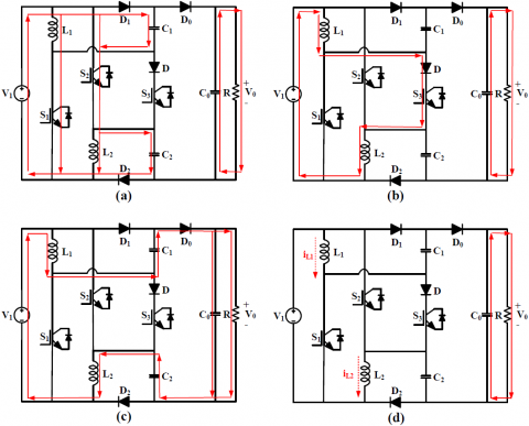
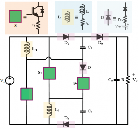
The circuit proposed in this paper is shown in the Figure2. This high-boost converter is based on bifurcated duty ratio technique (BDRT) along with the switched capacitors. There are three switches $S_1, S_2$ and $S_3$, two identical inductors $\mathrm{L}_1$ and $\mathrm{L}_2$ and two capacitors $\mathrm{C}_1$ and $\mathrm{C}_2$ connected to inductors with diodes $D_1$ and $D_2$ respectively. Also, there is output diode $\mathrm{D}_0$ and output capacitor $\mathrm{C}_0$.
Figure 2. Proposed High-Boost DC-DC converter
There is no mutual coupling between the two inductors. The inductors $\mathrm{L}_1, \mathrm{~L}_2$ and capacitors $\mathrm{C}_1, \mathrm{C}_2$ stores the energy and feed it to the output. The frequency of operation and time period are fs and $T_S$ respectively.
For simplification of the circuit analysis, the following assumptions are made:
- The inductor current is continuous due to high value of inductance.
- The capacitor voltage is assumed constant for one switching period due to high value of capacitance.
- All the components are considered ideal.
- The output voltage is constant.
- The inductors $\mathrm{L}_1$ and $\mathrm{L}_2$ are identical.
The operation of the given converter is shown in both continuous conduction mode (CCM) and discontinuous conduction mode (DCM). For the continuous mode of operation, there are three stages of operation and for the discontinuous mode, there are four stages.
2.1.1 CCM (Continuous Conduction Mode):
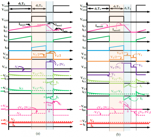
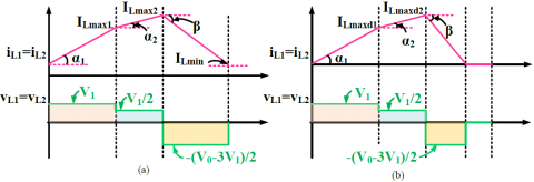
In CCM, the operation, the three stages are $d_1 T_s, d_2 T_S$ and $\left(1-\mathrm{d}_1-\mathrm{d}_2\right) \mathrm{T}_{\mathrm{s}}$. The inductor current is continuous and does not reach zero in the discharging mode. The demagnetizing angle is denoted by $\beta$. The minimum inductor current is $\mathrm{I}_{\mathrm{MN}}$.
The stages of operation of the proposed converter in $\mathrm{CCM}$ are discussed as follows:
Stage $1\left(0 \leq t \leq d_1 T_S\right)$: Figure3(a) represents the first operating stage of the converter. Here, the parallel switches $S_1$ and $S_2$ are switched on and the third switch $S_3$ is switched off. The inductors $L_1$ and $L_2$ are charged to source voltage $V_1$ through switch $S_1$ and $S_2$ in parallel. The diode $D_1$ and $D_2$ are conducting and charge the capacitors $\mathrm{C}_1$ and $\mathrm{C}_2$ to input voltage $V_1$. The typical operating waveform of the key components is shown in the Fig 4(a). The inductor currents $i_{L 1}$ and i i 2 increase linearly with a magnetizing angle $\alpha_1$ and $\alpha_2$ respectively and reaches to the maximum value equal to $I_{\operatorname{MAX} 1}$ and $\mathrm{I}_{\mathrm{MAX} 2}$. The inductors are identical and thus the magnetizing angle and maximum currents are equal. The variation of inductor current and voltages for CCM is shown in Figure5(a).
Figure 3. Stages of Operation (a) Stage 1, (b) Stage 2, (c) Stage 3 of CCM, (d) Stage 4 of DCM
Figure 4. Waveform of Key Elements (a) In CCM, (b) In DCM
Figure 5. Inductor Current and Voltage (a) In CCM, (b) In DCM
$V_L=V_{L 1}=V_{L 2}=V_1$ (1)
$V_{C 1}=V_{C 2}=V_1$ (2)
$V_{C 0}=V_0$ (3)
$I_L=I_{L 1}+I_{L 2}$ (4)
$\alpha_1=\tan ^{-1} \frac{I_{M A X 1}-I_{M I N}}{d_1 T_S}=\tan ^{-1}\left[L_1^{-1} V_1\right]$ (5)
$\alpha_1=\tan ^{-1}\left[L^{-1} V_1\right]$ (6)
Stage $2\left(0 \leq t \leq d_2 T_S\right)$: At the end of $\mathrm{d}_1 T_{\mathrm{S}}$, the parallel connected switches $S_1$ and $S_2$ are turned off and the switch $\mathrm{S}_3$ is turned on establishing a series connection between the two inductor and the input voltage. The equivalent circuit is shown in the Figure3(b). The inductors are charged in series and the input voltage is distributed equally to the inductors $L_1$ and $L_2$. The diodes $D_1$ and $D_2$ remain blocked and the capacitors remain charged to input voltage from the previous mode.
The inductor current increases further as shown in the waveform but the slope of the inductor current decreases due to the serial connection of the inductors. The inductor current slope is denoted by $\alpha_2$ for both the identical inductors $\mathrm{L}_1$ and $\mathrm{L}_2$ during time $\mathrm{d}_2 \mathrm{~T}_{\mathrm{s}}$.
$V_L=V_{L 1}=V_{L 2}=\frac{V_1}{2}$ (7)
$I_L=I_{L 1}=I_{L 2}$ (8)
$\alpha_2=\tan ^{-1} \frac{I_{M A X 2}-I_{M A X 1}}{d_2 T_S}=\tan ^{-1}\left[\frac{L_1^{-1} V_1}{2}\right]$ (9)
$\alpha_2=\tan ^{-1}\left[\frac{L^{-1} V_1}{2}\right]$ (10)
$\alpha_2=\frac{\alpha_1}{2}$ (11)
Stage $3\left(\left(d_1+d_2\right) T_S \leq t \leq T_S\right)$: In the last mode of operation, all the switches are off and the energy garnered in the inductors and capacitors is transferred to the load. The inductors $\mathrm{L}_1$ and $L_2$ reverses their polarity and the voltage of inductor comes in serial additive way along with the capacitor voltage and the input voltage yielding the high gain. The diodes $D_1$ and $D_2$ are reverse biased and diode $D_0$ is forward biased. The inductor current $I_{L 1}$ and $I_{L 2}$ is decreased linearly with slope $\tan \beta$ respectively where $\beta$ is the demagnetizing angle of inductor $\mathrm{L}_1$ and $\mathrm{L}_2$. The inductor and capacitor voltages and inductor current are given by equations below.
$V_L=V_{L 1}=V_{L 2}=\left(\frac{V_0-3 V_1}{2}\right)$ (11)
$I_L=I_{L 1}=I_{L 2}$ (12)
$\beta=\tan ^{-1} \frac{I_{M A X 2}-I_{M I N}}{\left(1-d_1-d_2\right) T_S}=\tan ^{-1}\left[\frac{V_0-3 V_1}{2}\right]$ (13)
$\beta=\tan ^{-1}\left[\frac{V_0-3 V_1}{2}\right]$ (14)
By charge balance equation for inductor $\mathrm{L}_1$,
$\int_0^{d_1 T_S} V_{L 1}+\int_0^{d_2 T_S} V_{L 1}+\int_0^{\left(1-d_1-d_2\right) T_S} V_{L 1}=0$ (15)
Solving the above equation,
$\frac{V_0}{V_1}=\left(\frac{3-d_1-2 d_2}{1-d_1-d_2}\right)$ (16)
And thus, the voltage gain ratio for $\mathrm{CCM}$ is given by,
$G_{C C M}=\left(\frac{3-d_1-2 d_2}{1-d_1-d_2}\right)$ (17)
Where $d_1$ is the duty ratio of switches $S_1$ and $S_2$
$\mathrm{d}_2$ is the duty ratio of switch $\mathrm{S}_3$,
$V_1$ is the input voltage,
$i_{L 1}$ is the current through inductor $L_1$,
$\mathrm{i}_{\mathrm{L} 2}$ is the current through inductor $\mathrm{L}_2$,
$\mathrm{V}_{\mathrm{C} 1}$ is the voltage across capacitor $\mathrm{C}_1$,
$\mathrm{V}_{\mathrm{C} 2}$ is the voltage across capacitor $\mathrm{C}_2$,
$V_{C 0}$ is the voltage across capacitor $C_0$,
$\mathrm{V}_0$ is the output voltage.
2.1.2 DCM (Discontinuous Conduction Mode)
In this mode, inductor current is reduced to zero before the end of discharging time and thus the discharging time is further split into two and forming total four operating stages as described below:
Stage $1\left(0 \leq t \leq d_1 T_S\right)$: This is similar to stage 1 of $\mathrm{CCM}$ and the peak inductor current at the end of this stage is $\mathrm{I}_{\mathrm{Lmaxd1}}$.
$I_{L 1(\max 1)}=I_{L 2(\max 1)}=I_{L \max d 1}$ (18)
$I_{L \max d 1}=\frac{V_1}{L} d_1 T_S=\tan \left(\alpha_1\right) d_1 T_S$ (19)
Stage $2\left(0 \leq t \leq d_2 T_S\right)$: This stage is also similar to stage 2 of CCM. In this the inductors are charged in series with switch $\mathrm{S}_3$. The inductor current reaches $\mathrm{I}_{\mathrm{Lmax} \mathrm{d} 2}$ during the time $\mathrm{d}_2 \mathrm{~T}_{\mathrm{s}}$.
$I_{l 1(\max 1)}=I_{L 2(\max 2)}=I_{L \max d 2}$ (20)
$I_{L \max d 1}=I_{L \max d 2}+\frac{V_1}{2 L} d_2 T_S=\frac{V_1}{L} d_1 T_S+\frac{V_1}{2 L} d_2 T_S$ (21)
Stage $3\left(0 \leq t \leq d_3 T_S\right)$: In this stage, the inductor current is reduced to zero. Here, in DCM it is denoted by $\mathrm{d}_3 \mathrm{~T}_{\mathrm{S}}$.
$I_{L \max d 2}=\left(\frac{V_0-3 V_1}{2 L}\right) d_3 T_S$ (22)
Stage $4\left(\left(d_1+d_2+d_3\right) T_S \leq t \leq T_S\right)$: In this stage, all the switches are already off and the current through the inductors is zero. The output capacitor $C_0$ feeds the load. By equating $I_{L \max 2}$ from stage 2 and stage 3,
$d_3=V_1\left(\frac{2 d_1+d_2}{V_2-3 V_1}\right)$ (23)
The average current across $\mathrm{C}_0$ can be stated as,
$I_{C_0}=\frac{\left(\frac{I_{L(\max 2)}}{2} d_3 T_S-I_2 T_S\right)}{T_S}$ (24)
Using above two equations,
$I_{C_0}=\frac{V_1^2\left(2 d_1+d_2\right)^2}{4 L\left(V_2-3 V_1\right)} T_S-\frac{V_2}{R}$ (25)
And
$I_2=\frac{V_2}{R}$ (26)
As the average current across $\mathrm{C}_0$ is zero in steady state, the above equation can be simplified as follow:
$V_2=\frac{V_1^2\left(2 d_1+d_2\right)^2}{4 \Gamma\left(V_2-3 V_1\right)}$ (27)
Solving the equation,
$G_{D C M}=\frac{3}{2}+\sqrt{\frac{9}{4}+\frac{\left(2 d_1+d_2\right)^2}{4 \Gamma}}$ (28)
Where $\Gamma=\mathrm{L} / \mathrm{RT}_{\mathrm{S}}$ is the normalized inductor time constant. For achieving desired value of voltage gain ratio in DCM, corresponding values of $d_1$ and $d_2$ need to be selected.
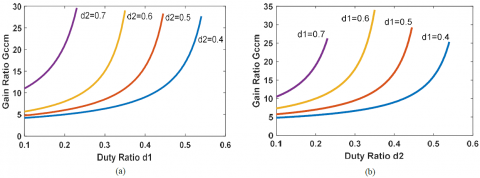
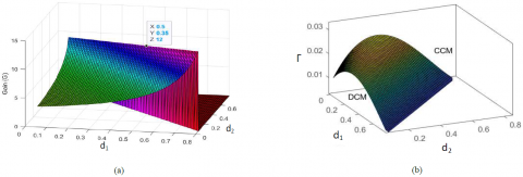
The variation of gain by varying one of the duty ratio while keeping the other constant is shown in the Figure6(a) and Figure6(b). The sum of duty ratio is taken less than $1 .$ $\left(\left(\mathrm{d}_1+\mathrm{d}_2\right)<0.85\right)$. This sum cannot be one because the energy stored in the passive elements must be transferred to load to uplift the gain. The three-dimensional variation of gain with two duty ratios is shown in Figure7(a) with the condition of $\left(\mathrm{d}_1+\mathrm{d}_2\right)<0.85$.
Figure 6. Variation of Gain $\mathrm{G}_{\mathrm{CCM}}$ with Duty Ratio (a) Gain $\mathrm{G}_{\mathrm{CCM}}$ with Duty Ratio $\mathrm{d}_1$ (b) Gain $\mathrm{G}_{\mathrm{CCM}}$ with Duty Ratio $\mathrm{d}_2$
Figure 7. (a). Variation of Gain $\mathrm{G}_{\mathrm{CCM}}$ with Duty Ratio $\mathrm{d}_1$ and $\mathrm{d}_2$, (b) Boundary Condition of operation depicting Inductor time-constant $\Gamma$ with $\mathrm{d}_1$ and $\mathrm{d}_2$
2.1.3 BCM (Boundary Conduction Mode)
In this mode of operation, the value of $T$ for boundary condition is obtained. In $\mathrm{BCM}$, the gain ratio obtained by $\mathrm{CCM}$ and DCM are equal. Thus, equating the Eq. 17 and Eq. 28,
$\frac{3-d_1-2 d_2}{1-d_1-d_2}=\frac{3}{2}+\sqrt{\frac{9}{4}+\frac{\left(2 d_1+d_2\right)^2}{4 \Gamma_B}}$ (29)
$\Gamma_B=\frac{\left(2 d_1+d_2\right)\left(1-d_1-d_2\right)^2}{4\left(3-d_1-2 d_2\right)}$ (30)
The surface of $\Gamma_{\mathrm{B}}$ is shown in the Figure7(b) for variation in values of $\mathrm{d}_1$ and $\mathrm{d}_2$ with the condition of $\left(\mathrm{d}_1+\mathrm{d}_2\right)<0.85$. For the converter to operate in CCM mode, it should have $\Gamma>\Gamma_{\mathrm{B}}$. The volume below the curved surface represents the $\mathrm{DCM}$ and the volume above represent CCM. For the converter to operate in CCM, the condition of $\Gamma$ is as follow:
$\Gamma>\frac{\left(2 d_1+d_2\right)\left(1-d_1-d_2\right)^2}{4\left(3-d_1-2 d_2\right)}$ (31)
3.1 Parameter Design
An appropriate designing of the converter parameters is essential for its enhanced performance. The DCM operation of the converter has certain drawbacks like discontinuous current, slower dynamic response, increased stress on semiconductor devices, etc. Therefore, it is desirable to operate the converter in CCM condition.
Inductor Design: the value of inductor $\mathrm{L}_1$ and $\mathrm{L}_2$ is same as inductors are assumed identical. The inductance value depends on maximum inductor voltage $\left(\mathrm{V}_{\mathrm{L}}\right)$, ripple current $\left(\Delta \mathrm{i}_{\mathrm{L}}\right)$, switching frequency $\left(\mathrm{f}_{\mathrm{S}}\right)$ and duty ratio $\left(d_1\right)$ for charging to maximum voltage. Thus, the inductance is given by the equation:
$L_1=L_2=\frac{V_L d_1}{\Delta i_L f_S}$ (32)
$L_1=L_2=\frac{V_1 d_1}{\Delta i_L f_S}$ (33)
This equation will give critical value of inductance and below this value, the converter will slip to DCM operating condition.
Capacitor Selection: The value of output capacitor $\mathrm{C}_0$ depends on output power $\mathrm{P}_0$, output voltage $\mathrm{V}_0$, ripple voltage across capacitor $\Delta \mathrm{V}_{\mathrm{C} 0}$ and switching frequency $\mathrm{f}_{\mathrm{s}}$.
$C_0 \geq \frac{P_0}{V_0 \Delta V_{C 0} f_s}$ (34)
The equation above given the critical value of output capacitance. The value of switched capacitor $C_1$ and $C_2$ will be equal and will be given by equation:
$C_1=C_2 \geq \frac{I_1 d_1}{\Delta V_{C 12} f_S}$ (35)
Where $I_1$ is the input current and $\Delta V_{C 12}$ is the ripple voltage across capacitor $\mathrm{C}_1$ or $\mathrm{C}_2$.
3.2 Voltage Rating of the Switch
The voltage stress on the switches and the diodes is shown in Figure4(a). The voltage rating of the switch is determined by the maximum voltage stress subjected to the switch which is given by the following equation:
$V_{S 1}=V_{S 2} \geq \frac{V_0}{2}$ (36)
$V_{S 3} \geq\left(\frac{G_{C C M}-2}{G_{C C M}}\right) V_0$ (37)
3.3 Voltage Rating of the Diode
The diode voltage stress on the diodes $D_1, D_2$ and $D_0$ is listed in Figure4(a). The diode rating given by the peak reverse voltage subjected to diode is given as follow:
$V_{D 1}=V_{D 2} \geq\left(\frac{G_{C C M}-1}{2 G_{C C M}}\right) V_0$ (38)
$V_{D 0} \geq\left(\frac{G_{C C M}-2}{G_{C C M}}\right) V_0$ (39)
3.4 Voltage Gain and Efficiency in Practical Conditions
Figure 8. Practical representation of Propounded Converter
The efficiency analysis is done by considering the practical condition of the converter circuit as depicted in Figure8. The inductors are assumed to be identical and the effective series resistance is represented by $r_{\mathrm{L}}\left(\mathrm{r}_{\mathrm{L} 1}=\mathrm{r}_{\mathrm{L} 2}=\mathrm{r}_{\mathrm{L}}\right)$. The diodes $D_1$ and $D_2$ are identical with forward voltage drop $V_{F D}$ and forward resistance drop $\mathrm{r}_{\mathrm{FD}}\left(\mathrm{V}_{\mathrm{FD} 1}=\mathrm{V}_{\mathrm{FD} 2}=\mathrm{V}_{\mathrm{FD}}\right.$ and $\left.\mathrm{r}_{\mathrm{FD} 1}=\mathrm{r}_{\mathrm{FD} 2}=\mathrm{r}_{\mathrm{FD}}\right)$. The capacitors $\mathrm{C}_1$ and $\mathrm{C}_2$ are also considered identical with equal voltage. All the switches $\mathrm{S}_1$, $S_2$ and $S_3$ are identical with on state resistance $r_s$. The diode $\mathrm{D}$ is neglected for simplicity. The output diode $\mathrm{D}_0$ is considered to have forward voltage drop $\mathrm{V}_{\mathrm{FD} 0}$ and forward resistance $\mathrm{r}_{\mathrm{FD} 0}$. The equations for inductor and capacitor voltage and current with considering the internal resistances and voltage drops are described below:
3.4.1 Mode 1
For the first mode, the average voltage and current across inductor are given as:
$V_L=V_1-i_L\left(r_S+r_L\right)$ (40)
$I_{C 1}=I_{C 2}=I_C=\frac{I_1-2 I_L}{2}$ (41)
$I_{C 0}=-\frac{V_0}{R}$ (42)
$V_C=V_1-V_{F D}-i_L\left(r_S+r_D\right)$ (43)
3.4.2 Mode 2
In the second mode, there is series charging of the inductor and the inductor voltage and capacitor current is given by:
$V_L=\frac{V_1-i_L\left(2 r_L+r_S\right)}{2}$ (44)
$I_{C 0}=-\frac{V_0}{R}$ (45)
3.4.3 Mode 3
In this mode when all the switches are off and the energy garnered in the passive elements are transferred to load.
$V_L=\frac{V_1-V_0+2 V_C-i_L\left(2 r_L+r_{D 0}\right)+V_{F D 0}}{2}$ (46)
$I_{C 0}=I_L-\frac{V_0}{R}$ (47)
By applying the ampere-second balance equation to the average output capacitor current,
$\int_0^{d_1 T_S} I_{C 0} d t+\int_0^{d_2 T_S} I_{C 0} d t+\int_0^{\left(1-d_1-d_2\right) T_S} I_{C 0} d t=0$ (48)
Solving the above equation:
$I_L=\frac{V_0}{R\left(1-d_1-d_2\right)}$ (49)
Applying voltage-second balance equation on the inductor voltage,
$\int_0^{d_1 T_S} V_L d t+\int_0^{d_2 T_S} V_L d t+\int_0^{\left(1-d_1-d_2\right) T_S} V_L d t=0$ (50)
Simplifying the above equation:
$\frac{V_0}{V_1}=\frac{\left(1+d_1\right)-\frac{V_{D 0}}{V_1}\left(1-d_1-d_2\right)}{\frac{2\left(d_1 A_1+d_2 A_2+A_3\right)}{R\left(1-d_1-d_2\right)}+\left(1-d_1-d_2\right)}+\frac{2 V_C}{V_1}$ (51)
Where
$A_1=r_S+\left(\frac{r_L}{2}-r_{D 0}\right)$ (52)
$A_2=\left(\frac{r_S+r_L-r_{D 0}}{2}\right)$ (53)
$A_3=\left(\frac{r_L+r_{D 0}}{2}\right)$ (54)
And
$\frac{V_C}{V_1}=\frac{V_1-V_{D 0}-i_D r_D-i_S r_S}{V_1}$ (55)
$\frac{V_C}{V_1}=1-\frac{V_{D 0}+i_D r_D+i_S r_S}{V_1}$ (56)
Where $\left(\mathrm{V}_{\mathrm{D}}+\mathrm{i}_{\mathrm{D}} \mathrm{D}\right)$ is the voltage drop across diode $\mathrm{D}_1$ or $\mathrm{D}_2$ and $i_S r_{\text {Son }}$ is the voltage drop across switch $S_1$.
3.5 Efficiency of the Converter
The efficiency of the given converter is calculated by the following equation:
$\eta=\frac{P_0}{P_0+P_{\text {Losses }}}$ (57)
For the computation of total losses, the loss of all passive components and switches is considered. The loss in the switches $\left(P_{\text {Loss }}^{S W}\right)$, losses in the diodes $\left(\Sigma P_{\text {Loss }}^{\text {Diodes }}\right)$, losses in the capacitors ( $\Sigma P_{\text {Loss }}^{\text {Capacitor }}$ ), and the inductor losses $\left(\Sigma P_{\text {Loss }}^{\text {Inductor }}\right)$ are taken into consideration. The total switch losses, switching losses and conduction losses of the switches are given by the equation below:
$P_{\text {Loss }}^{S W}=P_{\text {Switching }}^{S W}+P_{\text {Conduction }}^{S W}$ (58)
$P_{\text {Switching }}^{S W}=\sum_{k=1}^3 \frac{1}{6} V_B I_{D S}\left(t_{o n}+t_{o f f}\right) f_S$ (59)
Here, $V_B$ is the forward blocking voltage, $I_{D S}$ is the RMS current through the switch, $t_{\text {on }}$ and $t_{\text {off }}$ are the rise and fall times which can be found from the datasheet and $f_s$ is the switching frequency. For the conduction loss, the given formula is considered,
$P_{\text {Conduction }}^{S W}=\sum_{k=1}^3 R_{D S(O N)} I_{D S, r m s}^2$ (60)
The $R_{D S(O N)}$ is the on-state conduction resistance of the switch. For the diodes, the given formula is used for loss calculation,
$P_{\text {Loss }}^{\text {Diodes }}=R_{D 1} I_{D 1, r m s}^2+R_{D 2} I_{D 2, r m s}^2+R_{D 0} I_{D 0, r m s}^2$ (61)
Here, $R_D$ is the forward resistance of the diode. The power losses in the passive elements, inductors and capacitors are taken into account considering the equivalent series resistance of the capacitors and inductors.
$P_{\text {Loss }}^{\text {Capacitor }}=r_{C 1} I_{C 1 r m s}^2+r_{C 2} I_{C 2 r m s}^2+r_{C 0} I_{C 0 r m s}^2$ (62)
$\sum P_{\text {Loss }}^{\text {Inductor }}=r_{L 1} I_{L 1 r m s}^2+r_{L 2} I_{L 2 r m s}^2=2 r_L I_{L r m s}^2$ (63)
Here $r_C$ and $r_L$ are the equivalent series resistance of the capacitors and inductors respectively. The total loss is given by,
$P_{\text {Losses }}=P_{\text {Loss }}^{S W}+P_{\text {Loss }}^{\text {Diodes }}+P_{\text {Loss }}^{\text {Capacitor }}+P_{\text {Loss }}^{\text {Inductor }}$ (64)
Using Eq. 57 an efficiency of $92.6 \%$ is achieved at $200 \mathrm{~W}$. The variation of efficiency with power is as shown in the Figure11(a). For practical applications, electric vehicle work can be powered from $40 \mathrm{~kW}$ to more than $100 \mathrm{~kW}$. The proposed converter maintains higher efficiency even at high power rating because as stated in Eq.(57), even though the loss will increase but the percent loss will come down and the efficiency will be maintained.
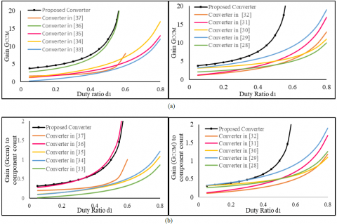
The proposed converter is compared with other converters that apply different techniques and various topologies. The converters from recent literature given in [25]-[37] are compared with the given topology. The various attributes taken into consideration are presented in Table 2. The proposed topology uses the bifurcated duty ratio and the high gain ratio is achieved without extreme value of duty cycle. The gain, gain to component count and ratio of switch voltage stress and the output diode voltage are listed for the particular converter. For a better insight to comparison, the graphs of variation of these parameters with duty ratio $d_1$ is shown in the Figure9. For the converters proposed in [36], [37] and the designed converter, the value of duty ratio $\mathrm{d}_2$ is considered an optimum value of $\mathrm{d}_2=0.35$ and with the constraint of $\mathrm{d}_1+\mathrm{d}_2<0.85$. The proposed converter is capable of providing gain of 12 times with duty ratio of $0.5$ and $0.35$. This implies that none of the switches is subjected to higher conduction time and thus, gets sufficient turn-off time which eliminates the reverse recovery problem. The gain of the proposed converter is higher than any of the listed converter topologies at a given duty ratio as can be seen in the Figure9(a). The converter in [28], also uses two inductors but they are charged in parallel and discharged in series. Though the number of components and switches are lesser, gain as well as gain to component count ratio is lesser along with considerably higher switch stress. In [29], switched capacitor technique is utilized to achieve the higher gain ratio. There are two switches with comparatively lesser stress but the gain is lesser. The hybrid converter proposed in [30] uses only single switch, but the gain provided by the converter considering the total number of components is lesser. In [31], the topology proposed is based on active switched inductor and passive switched capacitor with lesser number of switches and diodes and also lesser switch voltage stress but the drawback the lesser losses. An extendable converter with active-passive inductor cells (APIC) is proposed in [32]. With considering single unit of the extension cell, the number of components is high.
Figure 9. (a) Variation of gain $\left(\mathrm{G}_{\mathrm{CCM}}\right)$ and duty ratio $\left(\mathrm{d}_1\right)$; (b) Variation of gain to component count ratio $\left(\mathrm{G}_{\mathrm{CCM}} / \mathrm{TCC}\right)$ vs duty $\operatorname{ratio}\left(\mathrm{d}_1\right)\left[\right.$ where $\left.\mathrm{V}_{\mathrm{SN}}=\mathrm{V}_{\mathrm{SW}} / \mathrm{V}_0\right]$
Table 2. Comparison of proposed converter with other converter in recent literature
The advantage of the converter is that separate gate driver circuit is not required due to simultaneous operation of the switches and the increment in the number of the APICs reduces the voltage stress on the switches. The disadvantage of the given converter is lesser gain as compared to the number of components used. Similarly, in the converter in [33], higher number of components are utilized. This SEPIC based converter though uses only single switch but the number of inductors, capacitors and diodes are high, leading to low gain to component count ratio. The switch stress is a function of duty ratio and is equal to $\mathrm{V}_0 / 3 \mathrm{D}$. The converter in [34] is similar to [32] in structure comprising of extendable active-passive inductor cell (APICs). Here, the number of switches used is 3 , and the switch voltage stress is lesser at the cost of proliferation in the total number of components. In [35], a single switch with integrated with $\mathrm{L}^2 \mathrm{C}^3 \mathrm{D}^2$ is presented. It gives high gain with low voltage stress but the gain to component count is low as compared to proposed converter. The converters in $[28]-[35]$ use only single duty ratio and are not capable of providing higher gain to component count as compared to proposed converter. In [36] and [37], two duty ratios are used but the gain to component count of the proposed converter is lesser as shown in the Figure9(b). The converter in [36] show the gain ratio near to the proposed converter but in this the switch voltage stress in the diode voltage stress is higher. Thus, a better component utilization is done in the proposed converter. Thus, it can be concluded that the proposed converter is capable of providing very high gain without use of extreme duty ratio. This bifurcated duty ratio provides wide range of gain with lesser switch and diode voltage stress.
Also, it gives a wide range of variation of duty ratio thus controlling the dynamic operation of converter due to change in input or change in load.
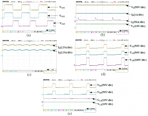
For the experimental verification, a $150 \mathrm{~W}$ prototype is designed. The switching frequency is $50 \mathrm{kHz}$. The gate pulses for the three switches are generated by the DSP controller integrated with code composer interface. The Texas F28335 is used in the experimental prototype. The components used are given in Table 3. The duty ratio of $0.5$ is used for the switches the $\mathrm{S}_1, \mathrm{~S}_2$ and $0.35$ for switch $\mathrm{S}_3$ as shown in the Figure10(a). With the input of $10 \mathrm{~V}$, $120 \mathrm{~V}$ output is obtained with output current of $1 \mathrm{~A}$ and load resistance of $120 \Omega$ as shown in the Figure10(b). The output is in accordance with the gain equation given in Eq.17. The input voltage equal to $10 \mathrm{~V}$ and input current of approximately $9 \mathrm{~A}$ is also shown in Figure10(b). (The ratio of output voltage to input voltage and output current to input current is same only for ideal conditions where there are no losses). The inductor currents $\mathrm{I}_{\mathrm{L} 1}$ and $\mathrm{I}_{\mathrm{L} 2}$ is $4.5 \mathrm{~A}$ approximately with two slopes of the increase in inductor current, $\alpha_1$ and $\alpha_2$ due to the two different charging paths of the inductor with bifurcated duty ratios between $\mathrm{S}_1, \mathrm{~S}_2$ and switch $\mathrm{S}_3$. The inductor current is equal in both the inductors because the inductors are identical and also connected in parallel with the input voltage source as shown in the Figure10(c). The capacitors $C_1$ and $C_2$ are charged to input voltage $\mathrm{V}_1$ equal to $10 \mathrm{~V}$.The voltage stresses of the switch $S_1$ and $S_2$ is equal to $V_1 / 2$ for the second mode in which only the switch $\mathrm{S}_3$ is $\mathrm{ON}$. In the third mode when all the switches are in off state, the voltage stress is equal to $50 \mathrm{~V}$. The voltage stress across $\mathrm{S}_3$ is $100 \mathrm{~V}\left(\mathrm{~V}_0-2 \mathrm{~V}_1\right)$.
Table 3. Parameter Tabulation
$\begin{array}{l|l}
\hline \text { Parameters } & \text { Values } \\
\hline \text { Input Voltage }\left(\mathrm{V}_1\right) & 10 \mathrm{~V} \\
\hline \text { Output Voltage }\left(\mathrm{V}_0\right) & 120 \mathrm{~V} \\
\hline \text { Duty Ratio }\left(\mathrm{d}_1 \text { and } \mathrm{d}_2\right) & 50 \%, 35 \% \\
\hline \text { Switches }\left(\mathrm{S}_1 \text { to } \mathrm{S}_5\right) & \text { IRF360 } \\
\hline \text { Diodes } \mathrm{D}_1, \mathrm{D}_0 & \text { MUR1560 } \\
\hline \text { Switching Frequency }\left(\mathrm{f}_{\mathrm{S}}\right) & 50 \mathrm{kHz} \\
\hline \text { Inductors }\left(\mathrm{L}_1 \text { and } \mathrm{L}_2\right) & \begin{array}{l}
360 \mu \mathrm{H} \\
(\text { Ferrite Core })
\end{array} \\
\hline \text { Capacitors }\left(\mathrm{C}_1, \mathrm{C}_0\right) & 10 \mu \mathrm{F}, 100 \mu \mathrm{F} \\
\hline
\end{array}$
Figure 10. (a). Variation of Gain $\mathrm{G}_{\mathrm{CCM}}$ with Duty Ratio $\mathrm{d}_1$ and $\mathrm{d}_2$, (b) Boundary Condition of operation depicting Inductor timeconstant $\Gamma$ with $\mathrm{d}_1$ and $\mathrm{d}_2$
Figure 11. (a). Variation of Efficiency (percent) with Power $P_0$ (b) Loss Distribution of the converter
In this paper, a novel topology of non-isolated high gain $\mathrm{DC}-\mathrm{DC}$ converter is proposed which has major advantage of providing considerably larger gain ratio without the use of coupled inductors, transformers, voltage multiplier units, etc. It uses novel bifurcated duty ratio (BDR) technique which helps in increasing the charging of inductor and hence the gain without using extreme duty ratio. The topology is proved economical because of wide variation of duty ratio, better gain to component ratio and decreased stress on the switches. The control of the given converter is simple and is capable of achieving wide range of gain with duty ratio. This topology can be used in renewable energy utilization for uplifting the output $\mathrm{DC}$ voltage. Moreover, integration of the green energy sources to micro-grids is one of the major applications where the proposed topology can find its application.
[1] C.T. Pan, C.-M. Lai, "A high-efficiency step-up converter with low switch voltage stress for fuel-cell system applications", IEEE Trans. Ind. Electron., vol. 57, no. 6, pp. 1998-2006, 2010.
[2] N. Eghtedarpour and E. Farjah, “Distributed charge/discharge control of energy storages in a renewable-energy-based DCmicro-grid,” IET Renewable Power Gener., vol. 8, no. 1, pp. 45–57, Jan. 2014
[3] .W. Li, W. Li, Y. Deng, and X. He, “Single-stage single-phase high-stepup ZVT boost converter for fuel-cell microgrid system,” IEEE Trans. Power Electron., vol. 25, no. 12, pp. 3057–3065, Dec. 2010.
[4] W. Li, W. Li, X. Xiang, Y. Hu, and X. He, “High step-up interleaved converter with built-in transformer voltage multiplier cells for sustainable energy applications,” IEEE Trans. Power Electron., vol. 29, no. 6, pp. 2829–2836, Jun. 2014.
[5] B. Axelrod, Y. Berkovich, A. Ioinovici, "Switched capacitor/switched inductor structures for getting transformerless hybrid DC–DC PWM converters", IEEE Trans. Circuits Syst. I Regul. Pap., vol. 55, no. 2, pp. 687-696, 2008.
[6] W. Li, J. Liu, J. Wu, and X. He, “Design and analysis of isolated ZVT boost converters for highefficiency and high-step-up applications,” IEEE Trans. Power Electron., vol. 22, no. 6, pp. 2363– 2374, Nov. 2007
[7] G. Chen, Y. Lee, S. Y. R. Hui, D. Xu, and Y. Wang, “Actively clamped bidirectional flyback converter,” IEEE Trans. Ind. Electron., vol. 47, no. 4, pp. 770– 779, Aug. 2000.
[8] H. Wu, K. Sun, L. Chen, L. Zhu and Y. Xing, "High Step-Up/Step-Down Soft-Switching Bidirectional DC–DC Converter With Coupled-Inductor and Voltage Matching Control for Energy Storage Systems," in IEEE Transactions on Industrial Electronics, vol. 63, no. 5, pp. 2892-2903, May 2016.
[9] R. Moradpour, H. Ardi, and A. Tavakoli, “Design and implementation of a new SEPIC-based high step-up DC/DC converter for renewable energy applications,” IEEE Trans. Ind. Electron., vol. 65, no. 2, pp. 1290–1297, Feb. 2018.
[10] H. Liu, H. Hu, H. Wu, Y. Xing, and I. Batarseh, “Overview of high-stepup coupled-inductor boost converters,” IEEE J. Emerg. Sel. Topics Power Electron., vol. 2, no. 3, pp. 689–704, Jun. 2016.
[11] A. Parastar and J. Seok, "High-Gain Resonant Switched-Capacitor Cell-Based DC/DC Converter for Offshore Wind Energy Systems," in IEEE Transactions on Power Electronics, vol. 30, no. 2, pp. 644-656, Feb. 2015.
[12] S. Park and S. Choi, "Soft-Switched CCM Boost Converters With High Voltage Gain for High-Power Applications," in IEEE Transactions on Power Electronics, vol. 25, no. 5, pp. 1211-1217, May 2010.
[13] S. Chen, T. Liang, L. Yang and J. Chen, "A Cascaded High Step-Up DC–DC Converter With Single Switch for Microsource Applications," in IEEE Transactions on Power Electronics, vol. 26, no. 4, pp. 1146-1153, April 2011, doi: 10.1109/TPEL.2010.2090362
[14] Y. M. Ye and K. W. E. Cheng, “Quadratic boost converter with low buffer capacitor stress,” IET Power Electron., vol. 7, no. 5, pp. 1162–1170, May 2014.
[15] M. Muhammad, M. Armstrong and M. A. Elgendy, "A Nonisolated Interleaved Boost Converter for High-Voltage Gain Applications," in IEEE Journal of Emerging and Selected Topics in Power Electronics, vol. 4, no. 2, pp. 352-362, June 2016
[16] N. Genc and I. Iskender, ``DSP-based current sharing of average current controlled two-cell interleaved boost power factor correction converter,'' IET Power Electron., vol. 4, no. 9, pp. 1015_1022, Nov. 2011.
[17] Prudente, L. L. Pfitscher, G. Emmendoerfer, E. F. Romaneli and R. Gules, "Voltage Multiplier Cells Applied to Non-Isolated DC–DC Converters," in IEEE Transactions on Power Electronics, vol. 23, no. 2, pp. 871-887, March 2008
[18] S. Padmanaban, M. S. Bhaskar, P. K. Maroti, F. Blaabjerg, and V. Fedák, ``An original transformer and switched-capacitor (T & SC)-based extension for DC-DC boost converter for high-voltage/lowcurrent renewable energy applications: Hardware implementation of a new T & SC boost converter,'' Energies, vol. 11, no. 4, p. 783, Apr. 2018.
[19] Y. Zhang, L. Zhou, M. Sumner, and P.Wang, “Single-switch,wide voltage gain range, boost DC– DC converter for fuel cell vehicles,” IEEE Trans. Veh. Technol., vol. 67, no. 1, pp. 134–145, Jan. 2018.
[20] M. M. H. Esmaeili, E. Babaei, and M. Sabahi, “High step-up quasi-Z source DC-DC converter,” IEEE Trans. Power Electron., vol. 33, no. 12, pp. 10563– 10571, Dec. 2018
[21] A. Ho, T. Chun, and H. Kim, “Extended boostactive-switched capacitor/switched-inductor quasi-Zsource inverters,” IEEE Trans. Power Electron., vol. 30, no. 10, pp. 5681–5690, Oct. 2015.
[22] B. Axelrod, Y. Berkovich, and A. Ioinovici, “Switched capacitor/ switched-inductor structures for getting transformerless hybrid dc-dc PWM converters,” IEEE Trans. Circuits Syst. I, Reg. Papers,vol. 55, no. 2, pp. 687–696, Mar. 2008.
[23] A. A. Fardoun andH. I. Esam, “Ultra step-up dc-dc converter with reduced switch stress,” IEEE Trans.Ind. Appl., vol. 46, no. 5, pp. 2025–2034, Sep./Oct. 2010.
[24] E. H. Ismail, M. A. Al-Saffar, A. J. Sabzali, and A. A. Fardoun,``A family of single-switch PWM converters with high step-up conversion ratio,'' IEEE Trans. Circuits Syst. I, Reg. Papers, vol. 55, no. 4, pp. 1159_1171, May 2008
[25] T. Cheng, D. D.-C. Lu, and L. Qin, ``Non-isolated single-inductor DC/DC converter with fully recongurable structure for renewable energy applications,'' IEEE Trans. Circuits Syst. II, Exp. Briefs, vol. 65, no. 3, pp. 351_355, Mar. 2018.
[26] F. Shang, G. Niu and M. Krishnamurthy, "Design and Analysis of a High-Voltage-Gain Step-Up Resonant DC–DC Converter for Transportation Applications," in IEEE Transactions on Transportation Electrification, vol. 3, no. 1, pp. 157-167, March, 2017.
[27] B. P. Baddipadiga and M. Ferdowsi, "A highvoltage- gain dc-dc converter based on modified dickson charge pump voltage multiplier," in IEEE Transactions on Power Electronics, vol. 32, no. 10, pp. 7707-7715, Oct. 2017.
[28] L. S. Yang, T. Liang, and J. Chen, “Transformerless DC–DC converters with high step-up voltage gain,” IEEE Trans. Ind. Electron., vol. 56, no. 8, pp. 3144–3152, Aug. 2009.
[29] Y. Tang, T. Wang and Y. He, "A Switched-Capacitor-Based Active-Network Converter With High Voltage Gain," in IEEE Transactions on Power Electronics, vol. 29, no. 6, pp. 2959-2968, June 2014, doi: 10.1109/TPEL.2013.2272639.
[30] B.Wu, S. Li,Y. Liu, andK.M. Smedley, “Anewhybrid boosting converter for renewable energy applications,” IEEE Trans. Power Electron., vol. 31, no. 2, pp.1203–1215, Feb. 2016.
[31] M. A. Salvador, T. B. Lazzarin, and R. F. Coelho, “High step-up DC–DC converter with active switched-inductor and passive switched-capacitor networks,” IEEE Trans. Ind. Electron., vol. 65, no. 7, pp. 5644–5654,Jul. 2018
[32] H. Mashinchi Maheri, E. Babaei, M. Sabahi and S. H. Hosseini, "High Step-Up DC–DC Converter With Minimum Output Voltage Ripple," in IEEE Transactions on Industrial Electronics, vol. 64, no. 5, pp. 3568-3575, May 2017, doi: 10.1109/TIE.2017.2652395.
[33] M. R. Banaei and S. G. Sani, "Analysis and Implementation of a New SEPIC-Based Single- Switch Buck–Boost DC–DC Converter With Continuous Input Current," in IEEE Transactions on Power Electronics, vol. 33, no. 12, pp. 10317-10325, Dec. 2018, doi: 10.1109/TPEL.2018.2799876
[34] E. Babaei, H. Mashinchi Maheri, M. Sabahi and S. H. Hosseini, "Extendable Nonisolated High Gain DC–DC Converter Based on Active–Passive Inductor Cells," in IEEE Transactions on Industrial Electronics, vol. 65, no. 12, pp. 9478-9487, Dec. 2018, doi: 10.1109/TIE.2018.2807367
[35] N. Elsayad, H. Moradisizkoohi and O. A. Mohammed, "A Single-Switch Transformerless DC--DC Converter With Universal Input Voltage for Fuel Cell Vehicles: Analysis and Design," in IEEE Transactions on Vehicular Technology, vol. 68, no. 5, pp. 4537-4549, May 2019, doi: 10.1109/TVT.2019.2905583.
[36] Bhaskar Ranjana, Mahajan & Meraj, Mohammed & Iqbal, Atif & Sanjeevikumar, P. & Pandav, Kiran & Alammari, Rashid. “High Gain Transformer-less Double-Duty-Triple-Mode DC/DC Converter for DC Microgrid”. IEEE Access. PP. 10.1109/ACCESS.2019.2902440,2019
[37] M. Lakshmi and S. Hemamalini, ``Nonisolated high gain DC-DC converter for DC microgrids,'' IEEE Trans. Ind. Electron., vol. 65, no. 2, pp. 1205-1212, Feb. 2018.