
Sifeddine Ayad* | Lynda Saci | Abdelmalek Khezzar
© 2026 The authors. This article is published by IIETA and is licensed under the CC BY 4.0 license (http://creativecommons.org/licenses/by/4.0/).
OPEN ACCESS
Digital control latency significantly influences the effectiveness of Insulated Gate Bipolar Transistor (IGBT) short‑circuit protection. This study experimentally investigates this influence by implementing an identical dual‑threshold di/dt‑based protection strategy on two digital platforms: an STM32F411CEU6 microcontroller unit (MCU) and an Altera Cyclone II Field Programmable Gate Array (FPGA). Both implementations share the same analog conditioning to ensure a fair comparison. Experiments were conducted at multiple DC‑link voltages; results at $\mathrm{V}_{\mathrm{DC}}=200 \mathrm{~V}$ using a K50T60 IGBT are presented as representative. The FPGA‑based implementation achieved a digital processing latency of 60 ns, compared with 298 ns for the MCU – a reduction of 240 ns. Under identical analog front‑end conditions, this latency difference contributed to a 57% decrease in peak short‑circuit current, a 45% reduction in fault duration, and a 76% decrease in estimated dissipated energy for the FPGA. Consequently, the protection safety margin relative to the device’s 5 µs short‑circuit withstand capability increased from 52.8% to 74.0%. These results indicate that, even when using a conventional Hall‑effect sensor (bandwidth 200 kHz), sub‑microsecond differences in digital control latency have a significant effect on fault mitigation performance under high di/dt conditions. The FPGA’s deterministic pipelined execution provides a quantifiable system‑level advantage over sequential microcontroller implementations within realistic industrial sensing constraints.
digital control architecture, di/dt detection, Field Programmable Gate Array, Insulated Gate Bipolar Transistor, latency, microcontroller, power electronics reliability, short-circuit protection
Insulated Gate Bipolar Transistors (IGBTs) serve as the backbone of modern power electronics, but exhibit critical vulnerability under short-circuit conditions. During hard-switching faults (type I), the collector current rises at rates exceeding $100 \mathrm{~A} / \mu s$, rapidly driving the device into saturation and threatening thermal destruction within the Short-Circuit Withstand Time (SCWT)—typically $5 \,\mu s$ for the K50T60. This severe fault induces localized hot spots and thermo-mechanical stress, leading to accelerated switching cell and wirebond degradation [1, 2]. Consequently, recent literature has heavily focused on hard-switching fault mitigation strategies that minimize the critical delay between fault initiation and gate turn-off [3]. Accurately capturing these extreme transients also dictates a strict consideration of sensor-bandwidth limits, as insufficient frequency response can severely distort the fault image and delay the protection logic [4].
Conventional desaturation (DESAT) protection monitors the collector-emitter voltage during the on-state. However, it requires blanking intervals of $1-3 \,\mu s$ to avoid nuisance tripping caused by Miller capacitance and high dv/dt effects during normal turn-on transients [5, 6]. These blanking times consume 20–60% of the available SCWT, leaving narrow safety margins. Single-threshold overcurrent detection reduces the blanking time but remains prone to false triggering due to parasitic inductances and electromagnetic interference, with response variability reaching several hundred nanoseconds [7].
di/dt-based strategies overcome these limitations by monitoring the current rise rate rather than its absolute magnitude. Using two thresholds ($i_{t h 1}$ and $i_{t h 2}$) combined with a timing window, they enable effective discrimination between normal switching transients and true short-circuit faults within sub-microsecond intervals [8-10]. Nevertheless, this temporal selectivity imposes severe constraints on the digital protection paths [11]. As advancements in fast gate drivers drastically reduce analog propagation delays [12], the bottleneck in fault-clearing time has shifted strictly to the digital controller. Microcontroller-based implementations execute protection decisions sequentially through interrupt service routines, where pipeline stalls, bus contention, and context switching introduce significant latency variations, typically ranging from 200 ns to over 1 µs. In contrast, Field Programmable Gate Arrays (FPGAs) implement the equivalent logic as pipelined hardware paths, achieving deterministic response times bounded by a fixed number of clock cycles—as low as (three pipeline stages at 50 MHz) in the Cyclone II implementation used in this study [11, 13].
Whether this architectural difference in latency and determinism materially affects IGBT survival under short-circuit stress remains experimentally unresolved. Prior studies have primarily focused on optimizing detection algorithms [8, 10] or validating single-platform implementations [14], without isolating the digital controller from variations in the analog front-end. This study addresses this gap by implementing an identical dual-threshold di/dt discrimination algorithm on an STM32F411CEU6 microcontroller unit (MCU) and an Altera Cyclone II FPGA, while maintaining strictly identical analog conditioning circuits, gate drivers, and power stage conditions. The objective is to quantify the influence of control latency and its variability on peak short-circuit current, fault duration, dissipated energy, and safety margin relative to the device SCWT.
Conventional desaturation (DESAT) and single-threshold overcurrent methods suffer from significant limitations, including blanking delays of $1-3 \,\mu s$ and high sensitivity to parasitic effects [5-7]. To overcome these drawbacks, this work adopts a dual-threshold di/dt discrimination approach. The following subsections detail the proposed algorithm and the two digital control platforms used for its implementation.
2.1 Conventional protection methods and their limitations
Conventional DESAT protection monitors the collectoremitter voltage $v_{C E}$ during the on-state, while single-threshold overcurrent detection compares the collector current against a fixed threshold. Both approaches require blanking intervals to avoid false triggering during normal switching transients. These delays, combined with sensitivity to parasitic inductances, $d v / d t$ noise, and temperature variations, reduce the effective safety margin relative to the device SCWT [5-7, 15, 16].
2.2 Proposed dual-threshold di/dt discrimination algorithm
The proposed protection uses a dual-threshold $\mathrm{di} / \mathrm{dt}$ discrimination algorithm. The collector current, sensed by a LEM LA-55P Hall-effect transducer (bandwidth 200 kHz ), is compared to two reference levels $i_{\text {th1}}$ and $i_{\text {th2}}$ using highspeed LM311 comparators. The threshold values, selected based on the expected di/dt during normal switching versus fault conditions, are presented in the experimental results Section.
The operating principle is as follows:
The short-circuit energy is calculated using Eq. (1)
$E_{s c}=\int_{t_{\text {init}}}^{t_{\text {int}}} v_{C E}(t) \cdot i_C(t) d t$ (1)
where, $t_{ {init}}$ and $t_{ {int}}$ are the fault initiation and interruption instants, respectively.
To ensure robust and early-stage detection of short-circuit faults, an early-fault detection strategy is implemented. The detection thresholds, $I_{t h 1}$ and $I_{t h 2}$, are governed by strict selection rules: they are set significantly lower than the nominal current rating $\left(I_{P N}=50 \mathrm{~A}\right)$, with the maximum threshold capped at 20 A.
In normal switching operation, the current commutation from the freewheeling diode to the IGBT begins with a very fast initial phase limited only by the stray inductance of the circuit. However, due to the limited bandwidth of the Hall-effect current sensor (200 kHz) and the associated analog conditioning circuit, the detection system cannot fully capture this extremely rapid transient. The observed current quickly transitions to a slower rise rate dictated by the load inductance. In contrast, during a hard short-circuit fault (Type I), the high di/dt persists because there is no load inductance to limit the current rise.
The timing window was therefore chosen independently of the load conditions. It is set to a fixed value well below the IGBT’s short-circuit withstand time (SCWT = 5 µs). For all tests, the timing window was fixed at 4 µs. This specific duration is translated into a strict digital counter limit within both the MCU and FPGA control architectures to guarantee precise temporal discrimination.
2.3 Digital control architectures: MCU versus FPGA
The same protection algorithm was implemented on two different digital platforms to evaluate the effect of control architecture on protection performance, and their characteristics are summarized in Table 1. The STM32F411CEU6 microcontroller (ARM Cortex-M4, 100 MHz) executes the detection through an interrupt service routine. The Altera Cyclone II FPGA (EP2C5T144C8, 50 MHz) implements the logic as a three-stage pipeline with registered stage boundaries, achieving deterministic latency bounded by a fixed number of clock cycles.
Table 1. Comparison of control architectures
|
Characteristic |
STM32F411CEU6 (MCU) |
Altera Cyclone II (FPGA) |
|
Processing paradigm |
Sequential (von Neumann) |
Spatially parallel (dataflow) |
|
Clock frequency |
100 MHz |
50 MHz |
|
Execution model |
Firmware (interrupt-driven) |
Synthesized hardware logic |
|
Latency source |
ISR entry + execution + context switching |
Combinational/registered logic delay |
|
Measured latency (Section 3) |
$298 \pm 20 \,n s$ |
$60+20 \,n s$ |
|
Latency variability (n = 10) |
$\pm 20 {~ns}$ |
Bounded (≤20 ns uncertainty) |
|
Flexibility |
High (software reprogrammable) |
Moderate (requires resynthesis) |
The MCU implementation exhibits variable latency depending on processor state, while the FPGA provides a cycle-bound response with a maximum asynchronous quantization uncertainty of 20 ns. Detailed latency measurements and variability analysis are presented in Section 3.
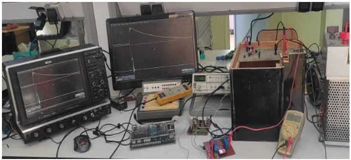
Figure 1 presents the experimental platform. A LeCroy Wave Runner 620Zi oscilloscope (500 MHz bandwidth, 2 GS/s sampling rate, 10-bit vertical resolution) was used for transient acquisition. A Keysight 33500B waveform generator provided the gate command at 1 kHz with 50% duty cycle. Collector-emitter voltage $v_{C E}$ and gate-emitter voltage $v_{G E}$ were measured using LeCroy PP023 500 MHz passive probes (10:1, 3.5 pF), while collector current was monitored by two LEM LA-55P Hall-effect sensors (bandwidth 200 kHz, rise time 1.8 µs). One sensor fed the protection circuit; the other, isolated via a 50 Ω termination, supplied the oscilloscope for independent waveform validation. The DC-link capacitor (5600 µF, 450 V) was pre-charged to the test voltage and disconnected from the supply during fault injection to eliminate source impedance variation.
To ensure a fair comparison, the entire analog signal chain—current sensor, comparators, and gate, gate driver, and power stage—remained strictly identical. Only the digital control unit (STM32F411CEU6 or Altera Cyclone II EP2C5T144C8) was interchanged via a pin-compatible header, with identical PCB trace lengths (±2 mm) for all critical paths.
Figure 1. Experimental setup consisting of the LeCroy 620Zi oscilloscope, voltage and current sensors, DC power supply, signal generator, and IGBT-based power stage. The digital controller (STM32F411 or Altera Cyclone II FPGA) is the only variable component between different tests, while all other hardware components remain unchanged
3.1 Command and protection circuit
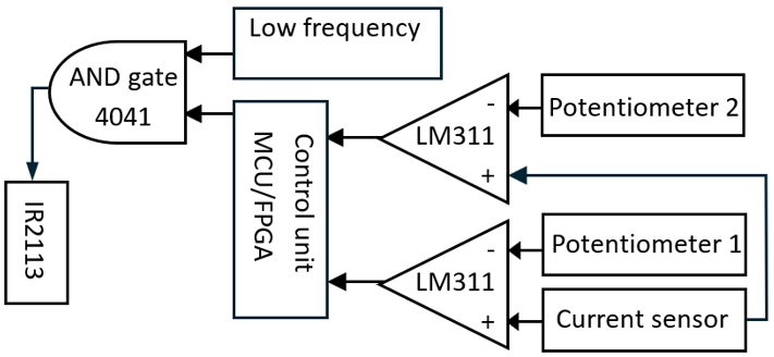
Figure 2 shows the block diagram. The collector current measured by the LEM LA-55P is converted to a voltage via a 0.5 Ω burden resistor and compared against two thresholds ($i_{t h 1}$ and $i_{t h 2}$) using LM311 comparators (response time 165 ns at 5 mV overdrive, datasheet value). The di/dt detection operates on the initial current slope before transducer saturation: the comparators trigger at approximately 10% and 90% of the expected fault current rise time, respectively. The digital controller processes comparator outputs and generates the active-low signal, which is combined with the PWM command via a 74HC08 AND gate before driving the IR2113 half-bridge gate driver.
Threshold Selection Methodology: Building upon the limitations of conventional DESAT and single-threshold methods discussed in Section 2.1, a dual-threshold di/dt approach was adopted. Thresholds were selected based on the expected di/dt discrimination requirements. For the K50T60 IGBT, hard-switching fault conditions produce a di/dt exceeding 200 A/µs. In normal inductive-load switching, the current commutation begins with a brief fast phase limited by stray inductance, but rapidly transitions to a much slower rise rate dictated by the load inductance.
To ensure robust discrimination, the timing window was chosen independently of the load conditions and fixed at 4 µs for all tests — a value well below the IGBT’s short-circuit withstand time (SCWT = 5 µs).
The timing window was calculated from:
$\Delta t_{ {win}}=\frac{I_{ {th} 2}-I_{ {th} 1}}{(d i / d t)_{ {fault,min}}}+t_{ {margin}}$ (2)
where, $(d i / d t)_{ {fault,min }}=200 {~A} / \mu {s}$ (conservative value at the lowest test voltage of 100 V), and $t_{ {comp,margin }}$ accounts for comparator propagation delay variation (±50 ns).
This ensures that any fault with di/dt ≥200 A/µs triggers both thresholds within the 4 µs window, while normal switching transients cannot reach $I_{t h 2}$ before the window expires.
Figure 2. Block diagram of the proposed protection and command circuit
Furthermore, the LEM LA-55P current sensor exhibits a stated response time of 500 ns to 1 µs to reach 90% of its nominal primary current (IPN = 50 A) at a di/dt of 200 A/µs. To significantly minimize the impact of this analog delay on the absolute detection accuracy, the fault detection thresholds Ith were deliberately constrained to less than half of the sensor's nominal range (with a maximum Ith of 20 A). This early-fault threshold selection guarantees that the protection triggers well before the sensor's maximum response time is reached, effectively mitigating the hardware delay during high di/dt fault dynamics.
3.2 FPGA pipeline architecture
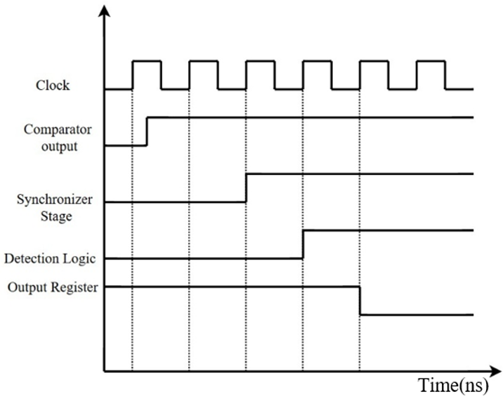
The Altera Cyclone II FPGA implements the protection logic as a three-stage pipeline operating at 50 MHz (clock period $T_{c l k}=20 \,n s$). Unlike the MCU's sequential interrupt-driven execution, the FPGA employs spatially parallel hardware with registered stage boundaries, achieving deterministic latency bounded by a fixed number of clock cycles.
Stage 1 — Synchronization: The two comparator outputs $\left(T H_1, T H_2\right)$, asynchronous to the 50 MHz clock, pass through a two-stage synchronizer comprising dual D-flip-flops per input. This stage consumes $2 \times T_{c l k}=40 n s$ and bounds the mean time between failures (MTBF) due to metastability to greater than $10^9$ years per the Cyclone II device handbook timing analysis [16]. Without synchronization, setup and hold violations could corrupt the detection logic.
Stage 2 — Detection Logic: The synchronized threshold signals feed a window comparator that asserts a window flag WIN if $T H_2$ occurs within the programmed $\Delta t_{ {win}}$ interval after $T H_1$. This combinational evaluation is registered on the next rising edge, consuming one clock cycle ($T_{c l k}=20 n s$). The detection logic is purely combinational between registers, with no feedback paths.
Stage 3 — Output Register: The final stage latches the FAULT signal with integrated glitch suppression. This registered output updates on the subsequent rising edge, consuming one additional clock cycle ($T_{c l k}=20 \,n s$).
The total pipeline latency is exactly $3 \times T_{c l k}=60 \,n s$. The throughput is one protection evaluation per $20 \,n s$, while the response latency remains fixed at $60 \,n s$ regardless of processor state. All pipeline registers use dedicated flip-flops within the Cyclone II logic elements; no combinational paths span multiple stages, eliminating race conditions.
The FPGA latency is highly bounded: the registered pipeline intrinsically consumes $60 \,n s$, with a maximum asynchronous quantization uncertainty of one clock period (20 ns) depending on the input phase relative to the 50 MHz clock, as illustrated in the detailed timing diagram in Figure 3. The MCU implementation, by contrast, uses GPIO inputs with internal Schmitt triggers and executes the protection decision through an interrupt service routine. Interrupt latency was minimized by configuring the EXTI line for rising-edge detection with the highest NVIC priority (preemption priority 0, sub-priority 0) and disabling all non-essential interrupts during tests.
Figure 3. Complete timing diagram of the Field Programmable Gate Array (FPGA)-based protection pipeline
3.3 Propagation delay characterization
The protection chain was deliberately assembled using standard industrial components rather than optimized laboratory-grade instrumentation. The LEM LA-55P Hall-effect transducer (bandwidth 200 kHz, rise time 1.8 µs) represents a conventional current sensor widely deployed in motor drives, inverters, and power conversion systems. Its bandwidth fundamentally limits the temporal fidelity of the measured current waveform—sub-microsecond transients are slewed and delayed. However, this limitation is intentional and methodologically controlled: since the sensor, analog conditioning, gate driver, and power stage remain strictly identical for both MCU and FPGA tests, the sensor-induced distortion constitutes a common-mode bias that cancels in the comparative analysis.
The objective of this study is not to optimize the entire protection chain, but to isolate the contribution of the digital controller under realistic, industrially representative conditions. The latency advantage measured between MCU and FPGA therefore reflects the architectural difference between sequential firmware execution and pipelined hardware logic, within the practical constraints of conventional Hall-effect sensing.
Component delays were characterized through datasheet extraction and oscilloscope measurement. The LEM LA-55P contributes no fixed delay but introduces bandwidth limitation; di/dt detection operates on the initial slope before transducer saturation. The LM311 comparator contributes 165 ns ($\pm 15 \,n s$ from temperature and overdrive variation). The 74HC08 AND gate contributes 7 ns ($\pm 1 \,n s$ at $\left(C_L=15 \mathrm{pF}\right)$). The IR2113 gate driver contributes 110 ns (±10 ns).
The control unit latency—the specific contribution isolated in this study—was measured as the interval between the 50% crossing of the LM311 output (test point TP1) and the 50% falling edge of FAULT (test point TP2), using the oscilloscope's built-in delay measurement with 50 ps resolution. This interval captures the digital controller's response time exclusively, excluding sensor and analog front-end delays, which are common to both implementations. Ten repetitions were performed per platform under identical fault conditions.
The MCU latency distribution (n = 10) yielded: mean = 298 ns, standard deviation = 20 ns, minimum = 264 ns, maximum = 352 ns. The propagation delay within the control unit is a critical factor in determining the response time of protection systems for power electronic devices. When utilizing a microcontroller like the STM32F411CEU6, operating at a maximum frequency of 100 MHz (Tcycle = 10 ns) [17], the measured 298 ns delay is primarily composed of hardware synchronization and software execution latencies. A cycle-level timing breakdown reveals that the interrupt entry latency intrinsically consumes 12 clock cycles, as defined by the Cortex-M4 architecture [18]. Furthermore, accessing the interrupt service routine from Flash memory at 100 MHz requires 3 wait states [19], adding pipeline flushing delays. The remaining cycles are consumed by APB/AHB bus synchronization, evaluating the detection logic (compiled with -O3 optimization for maximum speed), and asserting the GPIO output. Consequently, the total architectural latency for this sequential software-based implementation is bounded around 30 clock cycles (approx 300 ns).
The FPGA digital latency was verified to be bounded between 60 ns (best case) and 80 ns (worst case) across all ten repetitions, tracking the deterministic 60 ns pipeline delay and the maximum 20 ns asynchronous quantization uncertainty. The total protection response time sums all contributions for system-level context. The resulting delay budget is summarized in Table 2. The nominal 240 ns latency reduction achieved by the FPGA arises entirely from the architectural difference between pipelined hardware execution and sequential firmware execution. This difference is independent of the sensor bandwidth; a faster current transducer would preserve or amplify this architectural advantage, but would not alter the relative ranking of the two digital controllers. The corresponding impact of this latency reduction on short-circuit current and fault duration is presented in Table 3.
Table 2. Propagation delay budget of the protection chain
|
Component |
Delay (ns) |
Characterization Method |
|
LM311 comparator |
165 |
Datasheet, rated overdrive |
|
74HC08 AND gate |
7 |
Datasheet |
|
IR2113 gate driver |
110 |
Datasheet, turn-on propagation |
|
Control unit (STM32F411 MCU) |
298 |
Measured, Section 4 |
|
Control unit (Altera Cyclone II FPGA) |
60 |
Measured, Section 4 |
|
Total response time (MCU path) |
582 |
Sum of contributions |
|
Total response time (FPGA path) |
342 |
Sum of contributions |
Table 3. Peak short-circuit current and fault duration (mean ± std (95% CI), n = 10) (VDC = 200 V)
|
Reference Range (A) |
$i_{{th1}} / i_{ {th2}}$ (% ) |
$\Delta t$ (ns) |
$\mathrm{I}_{\text {peak,MUC }}$ (A) |
$I_{ {peak}, F P G A}$ (A) |
Reduction (%) |
$\mathrm{t}_{\text {fault}, \mathrm{MUC}}$ (µs) |
$t_{{fault}, F P G A}$ (µs) |
Reduction (%) |
|
15–20 |
75 |
230 |
144 ± 5 (140.4-147.6) |
62 ± 3 (59.8-64.1) |
56.9 |
2.36 ± 0.12 (2.27-2.44) |
1.30 ± 0.07 (1.25-1.35) |
44.9 |
|
11–15 |
73.33 |
110 |
132 ± 4 (129.1-134.9) |
54 ± 2 (52.6-55.4) |
59.1 |
2.06 ± 0.10 (1.9-2.1) |
1.23 ± 0.06 (1.18-1.27) |
40.3 |
|
8–10 |
80 |
25 |
116 ± 5 (112.4-119.6) |
49 ± 3 (46.8-51.14) |
57.8 |
1.86 ± 0.09 (1.79-1.92) |
1.14 ± 0.05 (1.10-1.17 |
38.7 |
|
5–8 |
62.5 |
45 |
109 ± 4 (106.1-111.9) |
46 ± 2 (44.6-47.4) |
57.8 |
1.76 ± 0.08 (1.70-1.81) |
0.90 ± 0.04 (0.87-0.92) |
48.9 |
3.4 Power stage
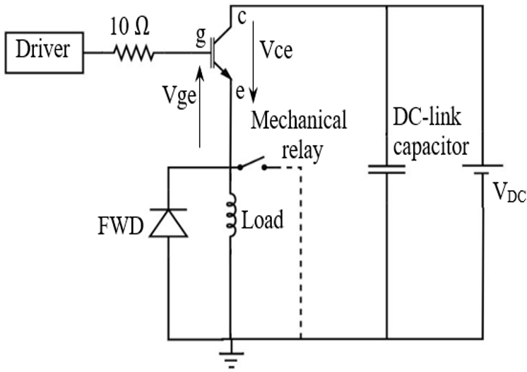
Figure 4 shows the IGBT power stage schematic. The setup uses a K50T60 IGBT (600 V / 50 A, TO-247 package), According to the manufacturer's datasheet, the K50T60 device has a guaranteed SCWT = $=5 \mu s$ at $T_j=15^{\circ} \mathrm{C}, V_{G E}=15 \mathrm{~V}, V_{D C}=400 \mathrm{~V}$ with an antiparallel MUR1560 fast-recovery diode. A 5 mH air-core inductor limits fault current rate of rise; a 5600 µF DC-link capacitor maintains voltage during the fault event. The fault is a Type-I hard-switching short-circuit. The mechanical relay closes to short-circuit the inductive load in parallel with the freewheeling diode. This directly applies the full DC-link voltage across the IGBT under test, inducing a high di/dt fault current. The gate resistance$R_G=10 \Omega$ (non-inductive, 1 W metal film) remained unchanged across all tests.
Figure 4. Schematic of the IGBT power stage used for short-circuit testing
Tests were conducted at DC-link voltages of 100 V, 200 V, and 400 V. Detailed results at 200 V are presented as representative. All tests were performed at ambient temperature $25 \pm 2{ }^{\circ} \mathrm{C}$ with forced air-cooling maintaining case temperature below $40^{\circ} \mathrm{C}$.
3.5 Protection algorithm and energy evaluation
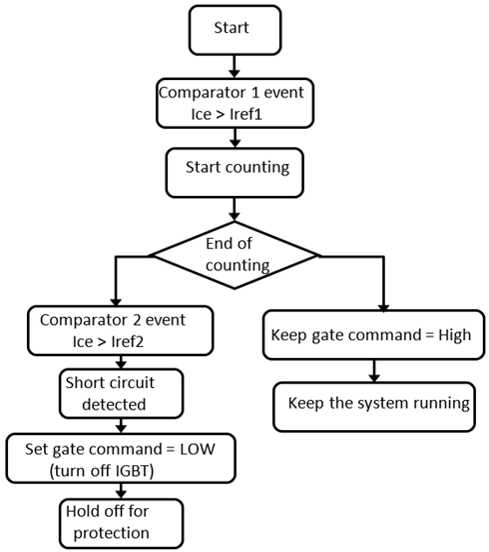
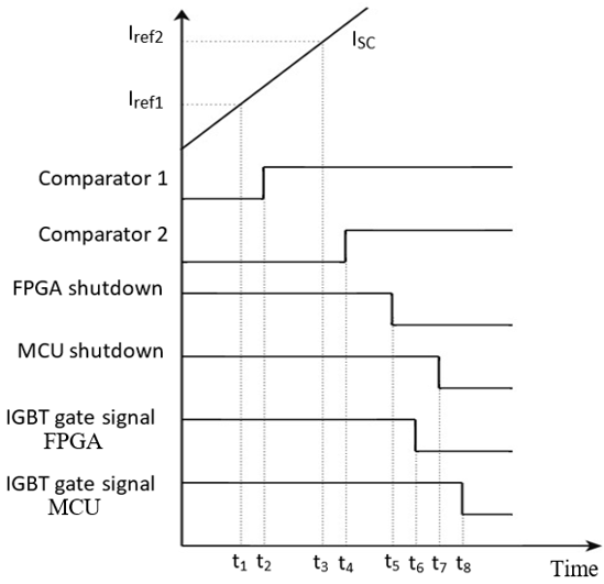
Figure 5 presents the protection algorithm flowchart. Figure 6 shows the timing diagram comparing the response of both controllers during a short-circuit event. The dissipated short-circuit energy is calculated offline from acquired waveforms using Eq. (1). Numerical integration uses the trapezoidal rule with oscilloscope samples (2 GS/s, $\Delta t=0.5 \,n s$). Waveforms were averaged over 10 shots per condition; standard deviation of $E_{S C}$ across shots was < 3% of the mean.
Figure 5. Flowchart of the proposed short-circuit protection
Figure 6. Timing diagram of a short-circuit event showing current evolution, comparator outputs, shutdown signals, and IGBT gate commands for both controllers
All reported results represent mean ± standard deviation of ten independent fault events per condition, separated by ≥ 30 s for thermal reset. To ensure the comparison is strictly architectural, the output-stage propagation delay was measured from the controller's FAULT pin to the initial $v_{C E}$ fall. With both platforms configured for maximum GPIO drive strength, this delay remained identical at approximately 117 ns. This confirms that the 240 ns performance advantage is exclusively due to the FPGA’s pipelined hardware execution, rather than varying output pin characteristics.
All experiments were conducted under the conditions described in Section 3. Each test condition was repeated ten times, and results are presented as mean ± standard deviation (n = 10). To strengthen the statistical analysis, 95% confidence intervals were calculated for all mean values using the t-distribution (df = 9) and are reported in Tables 3-5. Short-circuit tests were performed at DC-link voltages of 100 V, 200 V, and 400 V. Consistent relative trends were observed across all voltage levels; detailed results for 200 V are presented herein to avoid redundancy, while the comprehensive quantitative results for 100 and 400 voltage levels are summarized in Table 5.
Table 4. Dissipated energy and safety margins (mean ± std (95% CI), n = 10) (VDC = 200 V)
|
Reference Range (A) |
$E_{ {SC,MCU }}$ (mJ) |
$\mathrm{E}_{\text {SC,FPGA }}$ (mJ) |
Time-Based Margin MCU (%) |
Time-Based Margin FPGA (%) |
Energy-Based Margin MCU (%) |
Energy-Based Margin FPGA (%) |
|
15–20 |
33.98 ± 1.5 (32.90-35.05) |
8.06 ± 0.4 (7.77-8.34) |
52.8 |
74.0 |
92.6 |
98.2 |
|
11–15 |
27.19 ± 1.2 (26.33-28.05) |
6.64 ± 0.3 (6.42-6.85) |
58.8 |
75.4 |
94.1 |
98.6 |
|
8–10 |
21.58 ± 1.0 (20.86-22.29) |
5.59 ± 0.3 (5.37-5.80) |
62.8 |
77.2 |
95.3 |
98.8 |
|
5–8 |
19.18 ± 0.9 (18.53-19.82) |
4.14 ± 0.2 (3.99-4.28) |
64.8 |
82.0 |
95.8 |
99.1 |
Table 5. Peak short-circuit current and fault duration (mean ± std (95% CI), n = 10) (VDC = 100 V and 400 V)
|
Reference Range (A) |
DC−Link Voltage (V) |
$\mathrm{I}_{\text {peak,MUC }}$ (A) |
$I_{ {peak}, F P G A}$ (A) |
Reduction (%) |
$\mathrm{t}_{\text {fault}, \mathrm{MUC}}$ (µs) |
$t_{ {fault}, F P G A}$ (µs) |
Reduction (%) |
|
5–8 |
100 |
92 ± 3 (89.8-94.1) |
29 ± 2 (27.5-30.4) |
68.5 |
1.54 ± 0.08 (1.48-1.59) |
0.80 ± 0.04 (0.77-0.82) |
48.1 |
|
5–8 |
400 |
171 ± 7 (165.9-176) |
68 ± 3 (65.8-70.1) |
60.2 |
2.80 ± 0.13 (2.70-2.89) |
1.70 ± 0.07 (1.65-1.75) |
39.3 |
|
8–10 |
100 |
96.4 ± 4 (93.5-99.2) |
34.2 ± 2 (32.8-35.6) |
64.5 |
1.60 ± 0.06 (1.55-1.64) |
1.06 ± 0.05 (1.02-1.09 |
33.8 |
|
8–10 |
400 |
194 ± 7 (188.9-199) |
73.2 ± 3 (71-75.3) |
62.3 |
3.06 ± 0.15 (2.95-3.16) |
2.11 ± 0.10 (2.03-2.18) |
31.0 |
|
11–15 |
100 |
107 ± 4 (104.1-109.8) |
36 ±2 (34.5-37.4) |
66.4 |
1.80 ± 0.07 (1.74-1.85) |
1.12 ± 0.05 (1.08-1.15) |
37.8 |
|
11–15 |
400 |
247 ± 9 (240.5-253.4) |
89 ± 3 (86.8-91.1) |
64.0 |
3.40 ±0.16 (3.28-3.51) |
2.35 ± 0.12 (2.26-2.43) |
30.9 |
|
15–20 |
100 |
118 ± 4 (115.1-120.8) |
43 ± 2 (41.5-44.4) |
63.6 |
2.10 ±0.11 (2.02-2.17) |
1.19 ± 0.10 (1.118-1.262) |
43.3 |
|
15–20 |
400 |
264 ± 9 (257.5-270.4) |
110.6 ± 4 (107.7-113.4) |
58.1 |
3.90 ±0.18 (3.77-4.02) |
2.80 ± 0.14 (2.69-2.90) |
28.2 |
4.1 Normal operation validation
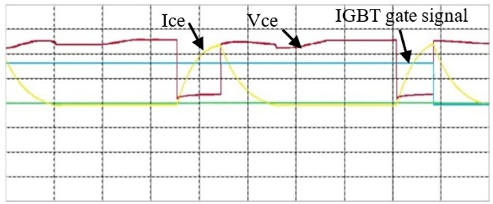
The protection system was first validated under normal PWM switching conditions with an inductive load. As shown in Figure 7, the gate signal remained active during normal transients, and no false protection triggering was observed. This confirms that the dual-threshold algorithm correctly distinguishes normal switching events from short-circuit faults. Validation tests were deliberately conducted at a 1 kHz switching frequency to prevent normal PWM turn-off from prematurely interrupting the short-circuit, ensuring the protection algorithm is the sole factor clearing the fault. Additionally, extensive testing across all DC-link voltages demonstrated complete robustness against nuisance tripping.
Figure 7. Validation waveforms under normal PWM switching conditions with inductive load. No false protection triggering is observed
It is worth noting that while rapid hard turn-off can induce $V_{C E}$ overshoots due to parasitic circuit inductance, the peak voltage in all experimental conditions remained strictly below the 600 V breakdown limit of the K50T60 device. Interestingly, the MCU implementation produced a higher peak $V_{C E}$ compared to the FPGA, primarily due to the significantly larger fault current accumulated prior to the delayed interruption. Consequently, both implementations maintained safe operation within the Reverse Bias Safe Operating Area (RBSOA).
4.2 Short-circuit performance comparison
Table 3 compares the peak short-circuit current and fault duration for both platforms at the representative DC-link voltage of 200 V across different threshold ranges. The control unit latencies, measured as the interval between comparator threshold crossing and shutdown signal assertion, were $298 \pm 20 \,n s$ for the MCU and $60+20 \,n s$ for the FPGA (mean ± std, n = 10), confirming the latency budget presented in Table 2. The FPGA achieves consistent reductions in peak current (57–59%) and fault duration (38–49%). The non-proportional relationship between latency improvement and fault duration reduction reflects the nonlinear IGBT current dynamics during desaturation.
4.3 Dissipated short-circuit energy and safety margins
The dissipated short-circuit energy was calculated using Eq. (1). Table 4 presents the mean energy values and the corresponding safety margins for both implementations.
To quantify the protection effectiveness, the time-based safety margin and the energy-based margin are defined and calculated using the following formulas:
Time-based margin $=\left(1-\frac{t_{\text {fault}}}{\mathrm{SCWT}}\right) \times 100 \%$ (3)
Energy-based margin $=\left(1-\frac{E_{S C}}{E_{\max}}\right) \times 100 \%$ (4)
where, $t_{\text {fault}}$ is the measured fault duration, $E_{S C}$ is the measured dissipated short-circuit energy, and $E_{\text {max}}$ is the critical allowable short-circuit energy limit derived from the device's SCWT rating.
To guarantee the accuracy of the $E_{S C}$ calculations, the energy was computed by integrating the instantaneous power from 10% of the peak current to the gate shutdown instant using carefully deskewed 2 GS/s waveforms. The overall measurement uncertainty is strictly bounded at ±6.5% (accounting for sensor bandwidth, probe calibration, and numerical integration), which confirms the high validity of the reported energy reductions.
4.4 Waveform analysis
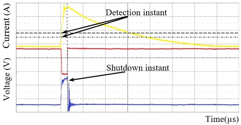
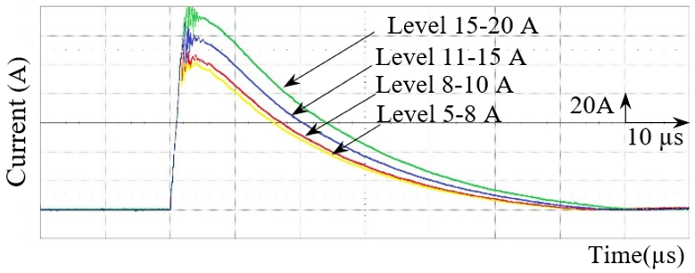
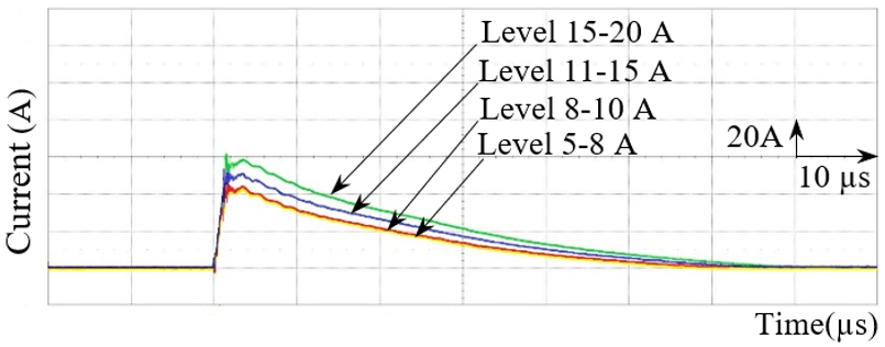
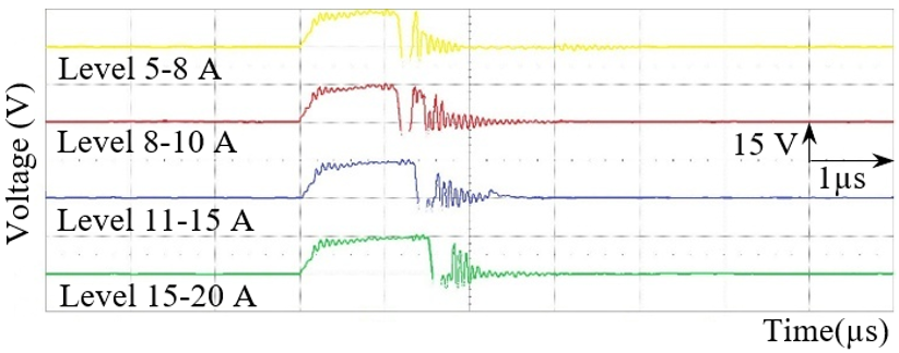
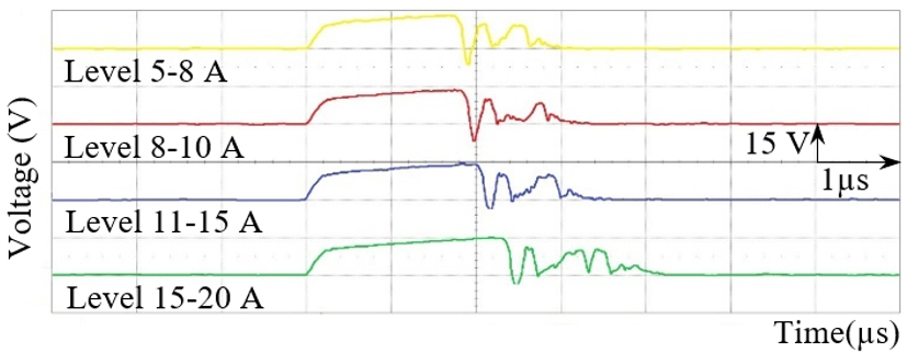
Figures 8-11 compare key waveforms under identical fault conditions (11–15 A threshold range). Figure 8 shows fault detection and shutdown instants. The FPGA detects the fault and asserts the shutdown signal 240 ns earlier than the MCU, consistent with the measured latency difference (Table 2). This temporal advantage translates directly into reduced current stress. Figure 9 presents collector current waveforms: MCU: Peak current reaches 132 A with a fault duration of $2.06 \,\mu s$. The slower response allows the current to rise further into saturation, increasing resistive losses. FPGA: Peak current limited to 54 A with a fault duration of $1.23 \,\mu s$. The earlier gate disable intercepts the current on its rising slope, before full desaturation.
Figure 8. Experimental short-circuit waveforms showing fault detection and gate shutdown instants for both MCU and Field Programmable Gate Array (FPGA) implementations (threshold range 15–20 A)
(a) MCU
(b) Field Programmable Gate Array (FPGA)
Figure 9. Collector current waveforms for MCU (top) and FPGA (bottom) under identical fault conditions
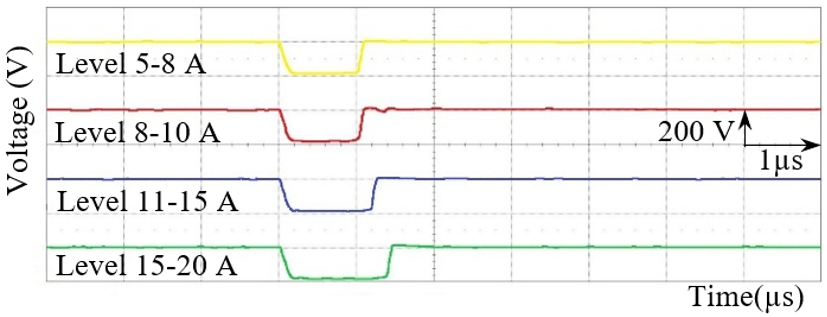
Figure 10 shows collector-emitter voltage: MCU: Higher $v_{C E}$ overshoot during turn-off due to larger interrupted current and longer fault duration. The energy dissipated during this phase contributes significantly to the total Esc.
FPGA: Reduced $v_{C E}$ overshoot reflecting lower energy dissipation at current interruption. The faster current decay limits the voltage spike amplitude.
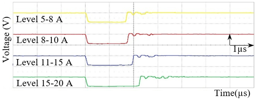
Figure 11 shows gate-emitter voltage during turn-off: MCU: Standard hard turn-off sequence. The gate discharge rate is limited by the IR2113 driver capability under high current conditions.
FPGA: Earlier initiation of turn-off sequence at lower current level. The gate reaches cutoff voltage faster, reducing the switching energy contribution to total dissipation.
These waveforms confirm that the 240 ns latency reduction is amplified by the high di/dt dynamics: the FPGA intercepts the fault earlier on the current slope, while the MCU allows the current to approach its saturation limit. The resulting differences in peak current (59% reduction), fault duration (40% reduction), and energy dissipation (76% reduction) are consistent with the quantitative data in Tables 3 and 4.
(a) FPGA
(b) MCU
Figure 10. Collector-emitter voltage waveforms for FPGA (top) and MCU (bottom) implementations
(a) FPGA
(b) MCU
Figure 11. Gate-emitter voltage waveforms for FPGA (top) and MCU (bottom) implementations
The experimental results in Section 4 show that the nominal 240 ns reduction in control latency achieved by the FPGA (342 ns vs 582 ns ) translates into substantial differences in IGBT stress metrics: peak current reduced by 57–59%, fault duration by 38–49%, and dissipated energy by 76%. Since the analog hardware chain and power stage were strictly identical, these differences are attributable to the digital controller's response time.
The non-proportional relationship between latency gain and current reduction (nominal 240 ns → 59% less current) reflects the high di/dt characteristic of short-circuit events. At $100 A / \mu S$, each nanosecond of additional delay allows 0.1 A of additional current. The FPGA's faster interception on the rising slope—before the current approaches its saturation limit—is the primary mechanism for the observed improvements.
5.1 FPGA latency advantage and its limits
The FPGA achieves lower latency through pipelined hardware execution: three registered stages consuming $60 \,n s$ at 50 MHz, without software overhead. This is inherently faster than the MCU's interrupt-driven sequence (ISR entry + context switching + execution ≈ $300 \,n s$).
However, it is important to clarify that the FPGA response is not entirely jitter-free; it exhibits a bounded asynchronous quantization uncertainty of up to one clock cycle (20 ns) due to the random arrival time of the asynchronous fault event relative to the 50 MHz sampling clock.
However, the measured repeatability of protection performance (Table 3) shows comparable standard deviations for both platforms (±2–5 A for peak current, ±0.04–0.12 µs for fault duration). This suggests that analog front-end variability (sensor noise, comparator threshold tolerance, IGBT parameter spread) significantly dominates over both the MCU's software jitter and the FPGA's bounded quantization uncertainty in the present setup. Consequently, the FPGA's theoretical determinism is masked by analog limitations at the system level.
5.2 MCU vs FPGA: Application-specific trade-offs
The choice between MCU and FPGA for IGBT protection depends on application constraints beyond raw latency:
5.3 Limitations and future work
Future work should include evaluation of modern FPGA platforms and extension to wide-bandgap devices such as SiC MOSFETs. The integration of soft turn-off techniques to further reduce voltage overshoot during fast interruption will also be investigated.
In summary, the choice of digital control architecture is not merely an implementation detail but a key design factor that directly influences IGBT reliability and protection effectiveness under short-circuit conditions.
|
Symbols |
|
|
$d i / d t$ |
Current rate of rise, A/µs |
|
$d v / d t$ |
Voltage rate of rise, V/µs |
|
$E_{ {max }}$ |
Critical allowable short-circuit energy limit, J |
|
Esc |
Dissipated short-circuit energy, J |
|
$i_C$ |
Collector current, A |
|
$I_{P N}$ |
Nominal primary current rating of the sensor, A |
|
$I_{S C}$ |
Short-circuit current, A |
|
$i_{t h 1}, i_{t h 2}$ |
First and second detection threshold currents, A |
|
$I_{ {peak }}$ |
Peak short-circuit current, A |
|
n |
Number of experimental repetitions |
|
$R_G$ |
Gate resistance, Ω |
|
$t_{ {fault }}$ |
Measured short – circuit fault duration, $\mu \mathrm{s}$ |
|
$t_{{init}}$ |
Fault initiation instant, s |
|
$T_{c l k}$ |
Clock period of the digital controller, ns |
|
$V_{C E}$ |
Collector-emitter voltage, V |
|
$V_{G E}$ |
Gate-emitter voltage, V |
|
$\Delta t_{ {win }}$ |
Timing window duration, s |
|
Acronyms |
|
|
DESAT |
Desaturation |
|
FPGA |
Field Programmable Gate Array |
|
IGBT |
Insulated Gate Bipolar Transistor |
|
MCU |
Microcontroller Unit |
|
PWM |
Pulse Width Modulation |
|
SCWT |
Short-Circuit Withstand Time |
|
RBSOA |
Reverse Bias Safe Operating Area |
|
SiC |
Silicon Carbide MOSFET |
[1] Numan, A.H., Hameed, A.Q. (2025). Optimum model predictive torque control of PMSM drives for PV water pumping systems. Journal Européen des Systèmes Automatisés, 58(9): 1975-1986. https://doi.org/10.18280/jesa.580919
[2] Kumar, D.G., Bhoopal, N., Ganesh, A., Sireesha, N.V., Rao, D.S.N.M. (2023). Implementation of an asymmetric multilevel inverter for solar photovoltaic applications using NR approach. Journal of New Materials for Electrochemical Systems, 26(1): 7-17. https://doi.org/10.14447/jnmes.v26i1.a02
[3] Lyu, G., Ali, H., Tan, H., Peng, L., Ding, X. (2024). Review on short-circuit protection methods for SiC MOSFETs. Energies, 17(17): 4523. https://doi.org/10.3390/en17174523
[4] Rafiq, A., Pramanick, S. (2022). Ultrafast protection of discrete SiC MOSFETs with PCB coil-based current sensors. IEEE Transactions on Power Electronics, 38(2): 1860-1870. https://doi.org/10.1109/TPEL.2022.3207594
[5] Qin, H., Hu, H., Huang, W., Mo, Y., Chen, W. (2022). An improved desaturation short-circuit protection method for SiC power modules. Energy Reports, 8: 1383-1390. https://doi.org/10.1016/j.egyr.2021.11.274
[6] Scholl, F., Fuhrmann, J., da Cunha, J., Eckel, H.G. (2021). A new robust short-circuit protection gate-driver circuit for IGBT with high desaturation current. In 2021 23rd European Conference on Power Electronics and Applications (EPE'21 ECCE Europe), Ghent, Belgium, pp. 1-10. https://doi.org/10.23919/EPE21ECCEEurope50061.2021.9570635
[7] Huang, X., Ji, S., Nie, C., et al. (2021). Comprehensive analysis and improvement methods of noise immunity of desat protection for high voltage SiC MOSFETs with high dv/dt. IEEE Open Journal of Power Electronics, 3: 36-50. https://doi.org/10.1109/OJPEL.2021.3134498
[8] Zhang, M., Li, H., Yang, Z., Zhao, S., Wang, X., Ding, L. (2024). Short circuit protection of silicon carbide MOSFETs: Challenges, methods, and prospects. IEEE Transactions on Power Electronics, 39(10): 13081-13095. https://doi.org/10.1109/TPEL.2024.3430897
[9] Meng, Z., Shi, F., Gao, Y., Hu, M. (2023). An improved protection circuit design for fast detection of short-circuit in IPM. IEEE Access, 11: 40430-40440. https://doi.org/10.1109/ACCESS.2023.3259460
[10] Xue, J., Xin, Z., Wang, H., Loh, P.C., Blaabjerg, F. (2020). An improved di/dt-RCD detection for short-circuit protection of SiC MOSFET. IEEE Transactions on Power Electronics, 36(1): 12-17. https://doi.org/10.1109/TPEL.2020.3000246
[11] Sha, Y., Wang, L., Zhou, M. (2024). Research on IGBT digital drive and protection technology based on FPGA. In: 2024 11th International Forum on Electrical Engineering and Automation (IFEEA), Shenzhen, China, pp. 1440-1443. https://doi.org/10.1109/IFEEA64237.2024.10878635
[12] Yuan, Q., Chen, Y., Liu, M. (2026). A 500kHz 600V capacitive isolated SiC converter with switching-on transition detection for hard-switching fault prognosis achieving 58ns short-circuit protection. In: 2026 Custom Integrated Circuits Conference (CICC), Seattle, WA, USA, pp. 1-4. https://doi.org/10.1109/CICC65509.2026.11509474
[13] Mocevic, S., Wang, J., Burgos, R., et al. (2020). Comparison and discussion on shortcircuit protections for silicon-carbide MOSFET modules: Desaturation versus Rogowski switch-current sensor. IEEE Transactions on Industry Applications, 56(3): 2880-2893. https://doi.org/10.1109/TIA.2020.2972816
[14] Vechalapu, K., Bhattacharya, S., Van Brunt, E., Ryu, S.H., Grider, D., Palmour, J.W. (2016). Comparative evaluation of 15-kV SiC MOSFET and 15-kV SiC IGBT for medium-voltage converter under the same dv/dt conditions. IEEE Journal of Emerging and Selected Topics in Power Electronics, 5(1): 469-489. https://doi.org/10.1109/JESTPE.2016.2620991
[15] Zhang, G., Shu, L., Zhang, J., Shao, S., Ke, J. (2023). A high speed short-circuit protection circuit with current limitation and soft turn-off for high power IGBTs. In: 2023 11th International Conference on Power Electronics and ECCE Asia (ICPE 2023-ECCE Asia), Jeju Island, Republic of Korea, pp. 3287-3293.
[16] Altera Corporation. (2008). Cyclone II device handbook, volume 1. Altera Corp. https://www.intel.com/content/dam/www/programmable/us/en/pdfs/literature/hb/cyc2/cyc2_handbook.pdf.
[17] STMicroelectronics. (2024). STM32F411xC STM32F411xE datasheet: Arm Cortex-M4 32b MCU+FPU, 125 DMIPS, 512KB flash, 128KB RAM (DS10314 Rev 8).
[18] STMicroelectronics. (2020). PM0214 programming manual: STM32 Cortex-M4 MCUs and MPUs programming manual (Rev 10).
[19] STMicroelectronics. (2025). RM0383 reference manual: STM32F411xC/E advanced Arm-based 32-bit MCUs (Rev 4).