Messaoud Makhlouf*![]() | Ouassim Laouar
| Ouassim Laouar![]()
© 2025 The authors. This article is published by IIETA and is licensed under the CC BY 4.0 license (http://creativecommons.org/licenses/by/4.0/).
OPEN ACCESS
In this paper, we compare three control strategies for a two-phase bidirectional interleaved DC–DC boost converter: classical Proportional–Integral–Derivative (PID) voltage control, a dual-loop PI scheme for voltage and current, and Model Predictive Control (MPC). Renewable energy systems, electric vehicles, and industrial power electronics widely use such converters, emphasizing the importance of stable operation, high efficiency, and fast dynamics. The practical question of which control strategy offers the best trade-off between simplicity, robustness, and performance motivates the study. To address this, we carried out simulations in MATLAB/Simulink under different conditions, including sudden changes in input voltage and load. The main performance indicators were response time, overshoot, steady-state error, and stability. Our findings show that open-loop control is unsuitable, as it leads to significant steady-state error and weak dynamic response. Single-loop PID improves accuracy but remains slow (~70 ms) and less robust. The dual PI controller eliminates steady-state error and overshoot, with a moderate response (~20 ms), which makes it attractive for general applications. MPC, however, achieves the strongest results: rapid response (~8 ms), no overshoot, negligible steady-state error, and excellent adaptability to load changes. The contribution of this study lies in its side-by-side evaluation of both classical and predictive controllers on the same converter platform. From a practical standpoint, dual-loop PI is recommended when cost and simplicity are priorities, while MPC is the preferred option for high-performance or time-critical systems.
interleaved DC–DC boost converter, single PID voltage control, dual PI control, Model Predictive Control (MPC), dynamic response analysis
The rising demand for efficient power conversion systems in renewable energy integration, electric vehicles (EVs), and industrial applications has propelled substantial developments in bidirectional DC–DC converter topologies and control methodologies. The bidirectional interleaved DC–DC boost converter has become a vital component owing to its capability for high voltage gain, reduced current ripple, and enhanced power density relative to traditional converters. Recent studies have highlighted these advantages [1]. The efficacy of these converters is significantly influenced by the control approach employed, which must guarantee rapid dynamic response, stability, and efficiency across diverse load conditions.
Despite extensive studies on converter topologies and individual control strategies, to the best of our knowledge, a unified comparative evaluation of PID, dual-loop PI, and MPC on the same bidirectional interleaved DC–DC boost converter platform has not been previously reported. This gap highlights the novelty of the present work, which systematically benchmarks these three control approaches under identical operating conditions.
Bidirectional converters are essential in contemporary energy systems, especially in applications necessitating energy transfer in both directions, including battery energy storage systems (BESS), vehicle-to-grid (V2G) systems, and hybrid renewable energy configurations. These applications are well documented in the literature [2]. The interleaved configuration optimizes performance by diminishing input current ripple, lowering inductor dimensions, and improving heat distribution. This improvement has been demonstrated in previous studies [3]. The advantages notwithstanding, the performance of interleaved converters depends heavily on the control strategy adopted, which necessitates a comprehensive comparative investigation of various methods.
Several control approaches have been suggested to manage bidirectional interleaved DC–DC boost converters, each possessing distinct merits and limitations. The principal strategies considered are summarized below.
1.1 Proportional–Integral–Derivative (PID) voltage regulation
PID controllers remain among the most widely utilized control strategies in power electronics, owing to their simplicity, ease of implementation, and established tuning methodologies. Their effectiveness and broad adoption have been well documented in the literature [4]. In bidirectional converters, PID controllers regulate the output voltage by altering the duty cycle in response to error feedback. Nonetheless, PID controllers show constraints in handling highly dynamic operating circumstances, such as abrupt load fluctuations or input voltage variations, frequently leading to overshoot, sluggish transient response, or instability. These limitations have been highlighted in prior research [5]. Furthermore, the fixed-gain characteristic of PID controllers may not efficiently adapt to changing system parameters, requiring advanced tuning or adaptive methods.
While PID controllers remain widely adopted for their simplicity, their limited ability to handle rapid disturbances has motivated the development of more advanced strategies, such as dual-loop PI control.
1.2 Dual proportional–integral loops for voltage and current regulation
To address the limitations of single-loop PID control, dual-loop PI control techniques have been formulated, integrating both voltage and current feedback loops, as demonstrated in the study [6]. The external voltage loop guarantees steady-state regulation, while the internal current loop improves dynamic response by managing inductor current ripple. This configuration enhances disturbance rejection and ensures superior stability during transient conditions. However, the tuning of dual-loop controllers is more complex, necessitating careful parameter selection to prevent interactions between the loops that may impair performance, as reported in the study [7]. In addition, their reliance on linear control theory may restrict efficacy in strongly nonlinear systems.
Despite these improvements, dual-loop designs introduce additional tuning complexity, prompting interest in alternative methods like Model Predictive Control (MPC), which offers systematic optimization under constraints.
1.3 Model Predictive Control (MPC)
Model Predictive Control (MPC) has emerged as a superior option for power electronics applications, due to its ability to handle system constraints and optimize control actions in real time, as shown in the study [8]. In contrast to conventional PI-based methods, MPC relies on a predictive model of the converter to anticipate its future behavior and select the optimal switching sequence. This predictive approach enhances dynamic response and reduces steady-state errors, as reported in the study [9]. Owing to these benefits, MPC has been increasingly applied in power converters and electric drive systems, where efficiency, fast dynamics, and robustness against parameter variations are critical. Nevertheless, MPC requires significant computational resources, demanding high-speed digital signal processors (DSPs) or field-programmable gate arrays (FPGAs) for real-time execution. Furthermore, its performance is highly dependent on the quality of the predictive model, making parameter sensitivity a critical concern, as discussed in the study [10].
Although extensive studies have examined these control strategies individually, a direct comparative analysis for two-phase bidirectional interleaved DC–DC boost converters remain limited, motivating the present work.
1.4 Research gap and objectives
A thorough evaluation of control techniques is crucial for identifying the most appropriate approach, taking into account the trade-offs between simplicity, dynamic performance, and computational burden. Although previous research has investigated individual control techniques, comprehensive comparative analyses focused specifically on bidirectional interleaved boost converters remain scarce.
This work aims to address this deficiency by:
Assessing the dynamic performance of PID, dual-loop PI, and MPC in terms of transient responsiveness, steady-state error, overshoot, and stability.
Evaluating robustness under diverse load and input voltage conditions.
Considering computational demands and feasibility of real-time implementation.
Providing criteria for selecting the most suitable control approach tailored to application-specific requirements.
The remainder of this paper is organized as follows:
Section~2 presents the topology and modelling of the bidirectional interleaved DC–DC boost converter.
Section~3 describes the design and implementation of the three control strategies.
Section~4 provides comparative simulation studies.
Section~5 concludes the work.
This study serves as a theoretical reference for enhancing the efficiency and reliability of bidirectional power converters in modern energy systems.
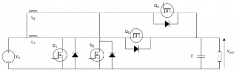
The boost converter illustrated in Figure 1 is a DC-DC power converter designed to increase (boost) the input voltage while proportionally reducing the output current. Its operation can be understood in two main states:
When the MOSFET switches (Q1, Q2) are turned ON, the inductors (L1, L2) store energy from the input source.
When the MOSFET switches (Q3, Q4) are turned ON, the inductors release their stored energy, which adds to the input voltage Vin, thereby boosting the output voltage Vout.
Figure 1. Interleaved boost converter
Interleaving is a control technique in which several converter phases operate in parallel, each with a phase-shifted switching cycle. By staggering the switching instants, the current ripples of individual phases partially cancel each other, leading to smoother input current, higher overall efficiency, and reduced electrical and thermal stress on the components.
A bidirectional converter, on the other hand, has the ability to transfer power in both directions, as seen in the study [11]. It operates in two modes:
Forward mode: energy flows from the input to the output.
Reverse mode: energy flows from the output back to the input.
This bidirectional capability is made possible by replacing conventional passive switches, such as diodes, with actively controlled semiconductor switches. Doing so not only reduces conduction losses caused by forward voltage drops but also enables controlled energy transfer in either direction, as shown in the study [12].
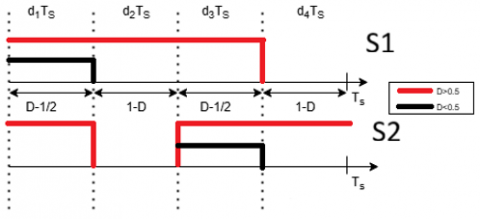
Figure 2. Switching states and corresponding duty-cycle intervals
From the diagram in Figure 2, we can observe that the switching signals of S1 and S2 are phase-shifted to ensure interleaving. Depending on the duty cycle D, two different operating cases are identified:
For D < 0.5, the conduction intervals of the switches partially overlap, leading to alternating conduction of the pairs (Q1, Q4) and (Q3, Q2).
For D > 0.5, the conduction intervals extend, and the switching sequence alternates between (Q1, Q2) and (Q3, Q4).
This phase-shifted operation distributes the current between phases, reduces input current ripple, and enables proper interleaving of the two converter legs.
Based on this diagram, the following relations can be established:
$d_1+d_2+d_3+d_4=\mathrm{D}$ (1)
$\frac{d X}{d t}=A X+B u$ (2)
$Y=C u$ (3)
With:
$C=\left[\begin{array}{lll}0 & 0 & 1\end{array}\right]$ (4)
$X=\left[\begin{array}{l}i_{L 1} \\ i_{L 2} \\ V_0\end{array}\right]$ (5)
$u=\left[V_{\text {in }}\right]$ (6)
Here, D represents the duty cycle over one switching period.
Based on the different switching states, the converter can operate in distinct modes, each described by its corresponding state-space matrices.
Mode 1 (Q1, Q4):
$A_1=\left[\begin{array}{ccc}0 & 0 & 0 \\ 0 & 0 & -\frac{1}{L_2} \\ 0 & \frac{1}{C} & -\frac{1}{R C}\end{array}\right]$ (7)
$B_1=\left[\begin{array}{c}\frac{1}{L_1} \\ \frac{1}{L_2} \\ 0\end{array}\right]$ (8)
Mode 2 (Q3, Q4):
$A_2=\left[\begin{array}{ccc}0 & 0 & -\frac{1}{L_1} \\ 0 & 0 & -\frac{1}{L_2} \\ \frac{1}{C} & \frac{1}{C} & -\frac{1}{R C}\end{array}\right]$ (9)
$B_2=\left[\begin{array}{c}\frac{1}{L_1} \\ \frac{1}{L_2} \\ 0\end{array}\right]$ (10)
Mode 3 (Q2, Q3):
$A_3=\left[\begin{array}{ccc}0 & 0 & -\frac{1}{L_1} \\ 0 & 0 & 0 \\ \frac{1}{C} & 0 & -\frac{1}{R C}\end{array}\right]$ (11)
$B_3=\left[\begin{array}{c}\frac{1}{L_1} \\ \frac{1}{L_2} \\ 0\end{array}\right]$ (12)
Mode 4 (Q1, Q2):
$A_4=\left[\begin{array}{ccc}0 & 0 & 0 \\ 0 & 0 & 0 \\ 0 & 0 & -\frac{1}{R C}\end{array}\right]$ (13)
$B_3=\left[\begin{array}{c}\frac{1}{L_1} \\ \frac{1}{L_2} \\ 0\end{array}\right]$ (14)
2.1 State-space averaging
State-space averaging offers a way to tame the complexity of switching converters by smoothing out their rapid on--off behavior. Instead of dealing with the fast, nonlinear, and time-dependent switching waveforms directly, this method replaces them with an averaged continuous-time model. In this model, the state equations describe how the system behaves over an entire switching period, while the matrices A and B are treated as constant within that interval, which has been discussed in the study [13]. The result is a simpler, Linear Time-Invariant (LTI) representation that is much easier to analyze and design controllers for.
Of course, this simplification comes with trade-offs. By averaging, the method overlooks what happens inside each switching cycle. That means it cannot capture high-frequency details such as switching noise caused by parasites, or ringing from LC resonances and transients. The model is reliable only for small variations around a steady operating point and assumes that the duty cycle changes slowly. Because it ignores current and voltage ripple, it may underestimate peak stresses on components an important factor when evaluating reliability. Finally, it loses accuracy altogether when the converter enters Discontinuous Conduction Mode (DCM). By using the switching states shown in Figure 2 and assuming D>0.5, the following mathematical equations can be derived:
$A_{\text {avg }}=\sum A_i \times d_i$ (15)
$B_{a v g}=\sum B_i \times d_i$ (16)
$A_{\text {avg }}=\left[\begin{array}{ccc}0 & 0 & \frac{D-1}{L_1} \\ 0 & 0 & \frac{D-1}{L_2} \\ \frac{1-D}{C} & \frac{1-D}{C} & -\frac{1}{R C}\end{array}\right]$ (17)
$B_{\text {avg }}=\left[\begin{array}{c}\frac{1}{L_1} \\ \frac{1}{L_2} \\ 0\end{array}\right]$ (18)
In order to obtain the transfer function relating the duty cycle to the output voltage, the governing equations are linearized around the steady-state operating point by introducing the following perturbations:
$i_{L 1}=I_{L 1}+\hat{\imath}_{I 1}$ (19)
$i_{L 2}=I_{L 2}+\hat{\imath}_{I 2}$ (20)
$D=D_{d c}+\hat{d}$ (21)
$V_o=V_o+\hat{V}_o$ (22)
Assuming that the perturbation in the input voltage Vin is negligible and substituting Eqs. (17)-(22) in Eq. (15) and write the differential equations. The system can be simplified, leading to the following expressions:
$\frac{d \widehat{l_{L 1}}}{d t}=\frac{D_{d c}+\hat{d}-1}{L_1}\left(V_o+\widehat{V}_o\right)+\frac{V_{i n}}{L_1}$ (23)
$\frac{d \widehat{l_{L 2}}}{d t}=\frac{D_{d c}+\hat{d}-1}{L_2}\left(V_o+\hat{V}_o\right)+\frac{V_{i n}}{L_2}$ (24)
$\begin{gathered}\frac{d \hat{V}_o}{d t}=\frac{1-D_{d c}-\hat{d}}{C}\left(I_{L 1}+\hat{\imath}_{L 1}\right)+ \\ \frac{1-D_{d c}-\hat{d}}{C}\left(I_{L 2}+\hat{\imath}_{L 2}\right)-\frac{1}{R C}\left(V_o+\hat{V}_o\right)\end{gathered}$ (25)
By rearranging the expressions and neglecting second-order terms, the following equations are obtained.
DC terms:
$\frac{D_{d c}-1}{L_1} V_o+\frac{1}{L_1} V_{i n}=0$ (26)
$\frac{D_{d c}-1}{L_2} V_o+\frac{1}{L_2} V_{i n}=0$ (27)
$\frac{1-D_{d c}}{C}\left(I_{L 1}+I_{L 2}\right)-\frac{1}{R C} V_o=0$ (28)
AC terms:
$\frac{d \widehat{\imath_{L 1}}}{d t}=\frac{\hat{d}}{L_1} V_o+\frac{D_{d c}-1}{L_1} \hat{V}_o$ (29)
$\frac{d \widehat{\imath_{L 2}}}{d t}=\frac{\hat{d}}{L_2} V_o+\frac{D_{d c}-1}{L_2} \hat{V}_o$ (30)
$\begin{gathered}\frac{d \widehat{V}_o}{d t}=-\frac{\hat{d}}{C}\left(I_{L 1}+I_{L 2}\right)+\frac{1-D_{d c}}{L_2}\left(\hat{l}_{L 1}+\hat{l}_{L 2}\right)-\frac{1}{R C} \hat{V}_o\end{gathered}$ (31)
By applying the Laplace transform in the AC term the following equations are obtained:
$p \times \widehat{l_{L 1}}=\frac{\hat{d}}{L_1} V_o+\frac{D_{d c}-1}{L_1} \hat{V}_o$ (32)
$p \times \widehat{l_{L 2}}=\frac{\hat{d}}{L_2} V_o+\frac{D_{d c}-1}{L_2} \hat{V}_o$ (33)
By summing Eqs. (32) and (33)
$\begin{aligned} p \times\left(\widehat{l_{L 1}}+\widehat{l_{L 2}}\right)= & \left(\frac{1}{L_1}+\frac{1}{L_2}\right) \hat{d} V_o +\left(\frac{1}{L_1}+\frac{1}{L_2}\right)\left(D_{d c}-1\right) \hat{V}_o\end{aligned}$ (34)
$\begin{gathered}p \times \widehat{V}_o=-\frac{\hat{d}}{C}\left(I_{L 1}+I_{L 2}\right)+\frac{1-D_{d c}}{L_2}\left(\hat{\imath}_{L 1}+\hat{\imath}_{L 2}\right) -\frac{1}{R C} \hat{V}_o\end{gathered}$ (35)
$I_{L 1}+I_{L 2}=I_{i n}=\frac{V_o}{R}$ (36)
By substituting Eqs. (34) and (36) in Eq. (34) we get the following result:
$\frac{\hat{V}_o}{\hat{d}}=\frac{R-p\left(L_1 L_2 V_o\right)+\left(1-D_{d c}\right)^2 V_o\left(L_1+L_2\right)}{p^2\left(R C L_1 L_2\left(1-D_{d c}\right)\right)+p\left(L_1 L_2\left(1-D_{d c}\right)\right)+R\left(L_1+L_2\right)\left(1-D_{d c}\right)^3}$ (37)
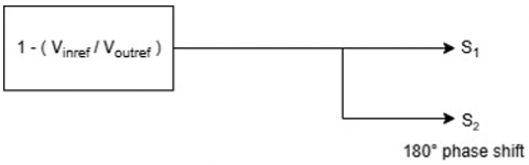
3.1 Open loop control
An open-loop system refers to a configuration in which the output is not fed back to regulate the input, its represented in Figure 3. In the present case, the duty cycle of the switches is predetermined based on theoretical calculations and is not dynamically adjusted according to the actual output voltage.
The duty cycle is determined using the conventional boost converter relation:
$V_{\text {out }}=\frac{V_{\text {in }}}{1-D}$ (38)
To guarantee interleaved operation, the switching signals are phase-shifted by
$\varphi=\frac{360^{\circ}}{N}$ (39)
where, N denotes the number of IBC phases.
Figure 3. Open loop basic control
In this study, the open-loop control is used as a worst-case reference to illustrate the limitations of an uncontrolled system, including large steady-state error, significant overshoot, and slow settling. In all figures and tables comparing control strategies, the open-loop performance is explicitly labeled as “Open-loop (worst case)” to clearly indicate its poor performance relative to the closed-loop and predictive controllers.
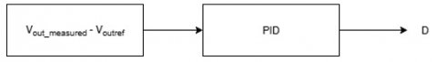
3.2 Voltage loop control
Voltage loop controls a single-loop feedback method that constantly checks the output voltage and compares it to a reference value. A voltage controller (PID in this case) processes the error signal and changes the duty cycle to maintain the output voltage at the desired level as represented in Figure 4. Then, the duty cycle is sent to the PWM generators, which are phase-shifted to ensure that the converter phases are properly interleaved, a method described in the study [14].
The error signal and the corresponding duty cycle are expressed as follows:
$e_v=V_{r e f}-V_o$ (40)
$D=f\left(e_v\right)$ (41)
For a PID controller, the duty cycle in the Laplace domain can be written as:
$D(s)=K_p \times e_v+\frac{K_i}{s} \times e_v+K_d \times s \times e_v$ (42)
The PID parameters were chosen through the pole placement method.
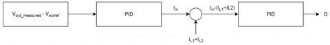
3.3 Double loop control
Double-loop control consists of two nested feedback loops: an inner current loop to enhance dynamic response and limit excessive current, and an outer voltage loop to regulate the output voltage, as reported in the study [15]. In Figure 5 the scheme senses the output voltage and compares it to a reference. A voltage controller then processes the voltage error to produce a reference current. The duty cycle is generated by the current controller processing the current error, which is obtained by comparing this reference with the sum of the inductor currents.
The PWM generators, phase-shifted to ensure proper interleaving, are then subjected to the duty cycle.
The error signal, reference inductor current, and duty cycle are expressed as follows:
$e_v=V_{r e f}-V_o$ (43)
$I_{i n}=f\left(e_n\right)$ (44)
In the Laplace domain, the reference current can be written as:
$I_{i n}(s)=K_p \times e_v+\frac{K_i}{s} \times e_v$ (45)
The current error is defined by:
$e_i=I_{i n}-\sum I_L$ (46)
$D=f\left(e_i\right)$ (47)
In the Laplace domain the duty cycle becomes:
$D(s)=K_p \times e_i+\frac{K_i}{S} \times e_i$ (48)
Figure 4. Voltage control principle
For the cascaded (double-loop) PID controller, a structured two-step manual tuning procedure was used. In the first stage, the outer voltage loop was adjusted to generate a current reference that closely matched the average input current under nominal conditions, ensuring stable voltage and proper power flow. In the second stage, the inner current loop was iteratively tuned by adjusting the proportional and integral gains to achieve fast dynamic response with minimal overshoot and satisfactory settling time.
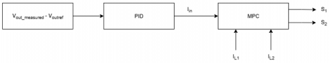
3.4 Finite control set model predictive control (FCS-MPC)
A predictive control technique called FCS-MPC was developed specifically for power electronic converters, whose switching states are discrete and finite rather than continuous. The FCS-MPC algorithm as represented in Figure 6 evaluates a cost function at each control cycle, predicts the system behavior for all possible switching states, and selects the switching state that minimizes the cost function, as shown in the study [16]. The process consists of four primary steps:
(i) extracting the converter's mathematical model;
(ii) forecasting future inductor current states;
(iii) evaluating a cost function;
(iv) selecting the switching state that minimizes the cost function.
The current tracking cost function is given by:
$J=w_i \sqrt{\sum\left(\frac{I_{r e f}}{N}-I_{L N}\right)^2}$ (49)
where, J is the cost function, Iref is the reference input current, N is the number of phases, ILN is the inductor current of the N-th phase, and wi is a weighting factor for current tracking. Minimizing this cost function ensures accurate current sharing among the converter phases while maintaining the desired output voltage regulation.
Unlike PID controllers, FCS-MPC does not rely directly on the exact converter parameters for its control decisions. This inherent feature makes it more robust to parameter mismatches, uncertainties, and load variations, thereby maintaining accurate tracking and stable operation even when component values deviate from their nominal values. However, this robustness comes at the expense of relatively high computational complexity, since the algorithm must evaluate all possible switching states at every sampling interval. This requirement increases execution time and places substantial demands on digital hardware. In practical implementations, real-time operation typically necessitates high-performance DSPs or FPGA platforms, where resource utilization and processing overhead become critical design considerations.
3.5 Design equations of interleaved boost converter (IBC)
The design of the IBC requires proper sizing of the inductors and capacitors to meet desired current ripple and voltage ripple specifications. The following relations are commonly used, which have been presented in prior research [17]:
$L \geq \frac{V_{\text {in }} \times D}{\Delta I_I \times f_{\text {switch }}}$ (50)
$C \geq \frac{V_{\text {in }} \times D}{\Delta V_o \times R \times f_{\text {switch }}}$ (51)
The main design parameters of the interleaved DC-DC boost converter are summarized in Table 1. These parameters define the operating conditions and provide the basis for simulation and controller design.
Table 1. Specifications of the two-phase interleaved boost converter
|
Vin |
Vout |
RLoad |
fswitch |
Iripple |
Vripple |
|
24 V |
220 V |
100 Ω |
10 KHz |
5% |
1% |
The design equations of the two-phase interleaved boost converter are given by [17]:
$L \geq 4.24 \times 10^{-3} H$
$C \geq 9.72 \times 10^{-6} F$
$I_L=\frac{I_{i n}}{2}$ (52)
$I_{\text {Lavg }}=\frac{I_{\text {out }}}{2 *(1-D)}$ (53)
The voltage control PID parameters are listed in Table 2.
Table 2. Voltage loop PID parameters
|
Kp |
Ki |
Kd |
N |
|
0.00014639 |
0.10587 |
3.7604e-08 |
250 |
The employed controller is a filtered discrete PID, whose transfer function is expressed as:
$\begin{aligned} P I D=K p+K i \times & T s \times \frac{1}{z-1} +K d \times \frac{N}{1+N \times T s \times \frac{1}{z-1}}\end{aligned}$ (54)
The double-loop control PI parameters are presented in Table 3.
Table 3. Voltage and current loop PI parameters
|
Control Loop |
Kp |
Ki |
|
Voltage PI |
0 |
35 |
|
Current PI |
0.05 |
0.1 |
The discrete PI controller is expressed as:
$P I=K p+K i \times T s \times \frac{1}{z-1}$ (55)
Finally, the PI parameters for the FCS--MPC-based voltage loop are summarized in Table 4.
Table 4. FCS--MPC-based voltage loop PI parameters
|
Kp |
Ki |
|
0 |
40 |
The tables summarize the converter specifications and controller parameters for the two-phase interleaved boost converter. Inductor and capacitor values were selected to satisfy the desired ripple limits and ensure proper energy storage. The discrete PID and PI controller formulations account for the sampling period, allowing straightforward digital implementation. The listed parameters enable each control strategy single-loop PID, double-loop PI, and FCS-MPC to achieve a balance between fast dynamic response, minimal steady-state error, and strong stability, supporting effective voltage regulation under varying load conditions.
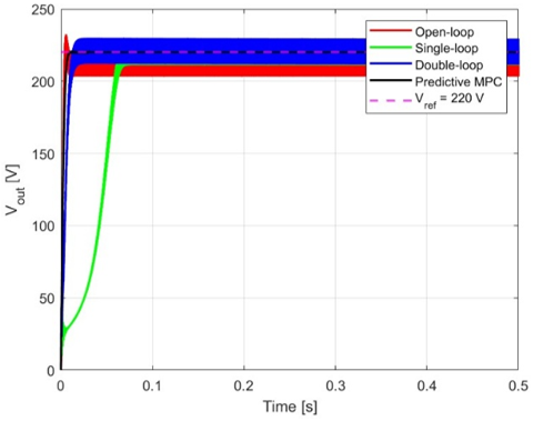
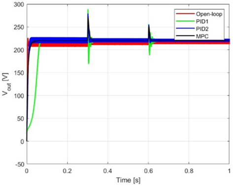
As expected, the open-loop case demonstrates poor voltage regulation, steady-state error, and ripple exceeding the 10% margin, confirming its role as a worst-case reference, and making it unsuitable for practical applications. The single-loop voltage control achieves regulation but with a slow response (~70 ms) and oscillations, indicating weak dynamic performance and suitability only where speed is not critical. The double-loopPI method significantly improves performance, reducing settling time to ~20 ms, eliminating overshoot, and providing strong stability, making it a good compromise for general-purpose use. In contrast, the FCS-MPC method delivers the best overall results, with the fastest response (~8 ms), negligible steady-state error, and very strong stability. Its ability to directly generate MOSFET switching signals explains its superior ripple suppression. However, this advantage comes at the cost of higher computational requirements and more complex switching frequency management. Overall, these results underline the trade-off between simplicity (single-loop PID), robustness (dual-loop PI), and superior dynamics (FCS-MPC). When considering quantitative stability metrics, the phase margin analysis confirms these observations: the open-loop system is unstable with a -90° phase margin, the voltage control loop is moderately stable at 60°, the double-loop PI achieves very strong stability at 89.9°, and the FCS-MPC reaches an almost ideal 90° phase margin, reinforcing its superior dynamic performance.
Figure 7. Output voltage for different control methods. The open-loop case is a benchmark (worst-case) and shows poor regulation compared to closed-loop methods
Figure 7 compares the output voltage of the converter under different control strategies. The comparison is summarized in Table 5.
Table 5. Comparative performance of different control methods
|
Control Method |
Open Loop (Unstable) |
Voltage Control |
Double Loop PI |
FCS-MPC |
|
Overshoot |
10% |
0% |
0% |
0% |
|
Response time |
10ms |
70ms |
20ms |
8ms |
|
Steady state error |
10% |
0 |
0 |
0 |
|
Stability phase margin |
-90° |
60º |
89.9º |
90º |
|
Remarks |
Benchmark (Worst case) |
Closed-loop baseline |
Improved dynamics |
Best overall |
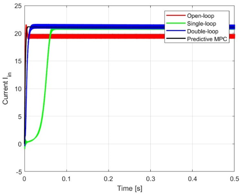
Figure 8 compares the input current response of the interleaved boost converter under different control methods.
It is evident from this figure that the open-loop method fails to achieve accurate current regulation, maintaining a steady-state offset relative to the reference. This confirms its role as a worst-case benchmark for highlighting the superior tracking accuracy of the closed-loop strategies.
With voltage control, the current slowly converges toward the reference but requires more than 0.07 seconds to reach steady state. The slow approach to the final value is evident, illustrating the limited dynamic behavior of this method.
Figure 8. Input current for different control methods. The open-loop case is a benchmark (worst-case) and performs poorly compared to closed-loop method
The double-loop PI strategy provides a faster and more accurate response. Here, the current reaches the reference within about 0.02 seconds, settling smoothly with minimal error and without significant deviations. The trajectory is clearly quicker and more stable compared to the open-loop and voltage control cases.
The predictive control (FCS-MPC) achieves the best performance overall. The current rises rapidly, reaching the reference in less than 0.01 seconds with negligible overshoot, practically no oscillations, and excellent steady-state accuracy, making it the most effective strategy in this comparison, as shown in the study [18].
Figure 9 shows the voltage response when the reference changes from 220 V to 100 V. As expected, the open-loop response shows poor voltage regulation and overshoot, highlighting its role as a worst-case benchmark for comparison against the closed-loop strategies. The PID controllers (single loop and double loop) track the new reference with noticeable overshoot and slower settling. In contrast, the MPC method provides the fastest adjustment with minimal overshoot and excellent steady-state accuracy, confirming its superior performance under variable reference conditions.
Figure 9. Voltage response to variable reference (220 V -100 V). The open-loop case is a benchmark (worst-case) and shows poor regulation versus closed-loop methods
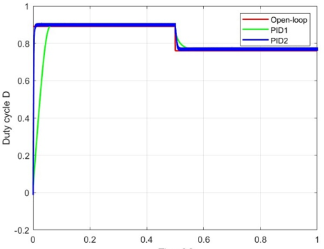
Figure 10. Duty cycle variation for open-loop, PID1, and PID2. The open-loop case is a benchmark (worst-case) and shows poor control versus closed-loop methods
Figure 10 shows the duty cycle variation for open-loop, PID1 (single-loop), and PID2 (double-loop) control methods. The open-loop which is included only as a benchmark (worst-case), maintains a fixed duty cycle with no corrective adjustment, which can lead to large voltage and current deviations across the MOSFETs, potentially increasing device stress. By using Taylor expansion, we can arrive at the following equations:
$\Delta V_{D S}(t) \approx \frac{\partial V_{D S}}{\partial D} \Delta D(t)$ (56)
$\Delta I_D(t) \approx \frac{\partial I_D}{\partial D} \Delta D(t)$ (57)
which directly affect EMI increasing it since:
$E M I \propto \frac{d V_{D S}}{d t}+\frac{d I_D}{d t} \approx \frac{\partial V_{D S}}{\partial D} \frac{d D}{d t}+\frac{\partial I_D}{\partial D} \frac{d D}{d t}$ (58)
PID1 regulates the duty cycle to reach the reference but exhibits slower convergence and slight deviations during transients, resulting in moderate MOSFET stress and EMI. In contrast, PID2 ensures faster and more stable duty cycle adjustment, maintaining closer alignment to the desired operating point. This reduces both transient voltage/current excursions and the rate of change of switching signals, thereby minimizing MOSFET stress and EMI while providing better dynamic performance.
Figure 11 illustrates the output voltage response of the converter under varying load conditions (100 ohms, 150 ohms, and 200 ohms). The open-loop case, included only as a benchmark (worst-case), fails to regulate the voltage, showing poor stability, large deviations and poor disturbance rejection. PID1 (voltage control) achieves regulation but with noticeable oscillations and slower recovery after load changes. PID2 (double-loop control) improves disturbance handling, offering faster recovery and better damping. In contrast, the MPC method provides the most robust performance.
Figure 12 shows the input current response under varying load conditions (100 ohms, 150 ohms, and 200 ohms). The open-loop case, included only as a benchmark (worst-case), fails to adapt properly to the load change, leading to poor current regulation and deviation from the expected value. PID1 responds but with slower dynamics and higher oscillations during transients. PID2 (double-loop control) provides improved disturbance rejection, ensuring smoother transitions and reduced ripple. The MPC method again demonstrates the best performance, maintaining stable current with the fastest recovery and minimal overshoot across all load variations.
Figure 11. Output voltage under load variation (100 Ω to 200 Ω). The open-loop case is shown as a benchmark and exhibits poor regulation versus closed-loop controllers
Figure 12. Input current response to load variation (100 Ω to 200 Ω). The open-loop case is a benchmark (worst-case) and performs poorly versus closed-loop methods
In this study, different control strategies for two phases interleaved boost converter were evaluated using key performance metrics, namely response time, overshoot, and steady state error.
The open loop control is unsuitable for high performance applications dues to its large steady-state error, significant overshoot and inability to track reference voltage accurately. These shortcomings lead to large deviations in both voltage and current, as well as poor settling under load variations.
The single-loop voltage control achieves excellent steady-state accuracy; however, its long response time (~70 ms) makes it appropriate only for applications where speed is not critical. Furthermore, its moderate stability limits its effectiveness in systems requiring fast dynamic response.
Double loop control offers a more balanced solution by eliminating steady-state error and overshoot while maintaining a moderate response time (~20 ms). Its strong stability and robust performance make it a better choice for a wide range of general-purpose systems.
Finally, the predictive control (FCS-MPC) method demonstrates the best overall performance, with the fastest response (~8 ms), zero overshoot, negligible steady-state error, and strong adaptability to load changes. These features establish predictive control as the most suitable choice for high-performance, time-critical applications where minimal transients are essential. While double-loop control remains a reliable alternative for general use, single-loop voltage control and open-loop control are not recommended in scenarios where performance and stability are critical.
However, it is important to note that FCS-MPC incurs higher computational complexity due to real-time optimization at each sampling step, which increases execution time and requires more DSP or FPGA resources. Therefore, while ideal for high-performance applications, its hardware and software demands must be considered, and in resource-constrained systems, simpler double-loop or single-loop controls may be more practical.
It should also be noted that the simulations in this study are idealized. In practical implementations, factors such as measurement noise, parameter drift, and component tolerances can affect performance. Future work could focus on enhancing robustness against these non-idealities, for example by incorporating adaptive or observer-based techniques, sensor filtering, and calibration strategies to maintain accurate control under real-world conditions.
[1] Hashemzadeh, S.M., Al-Hitmi, M.A., Aghaei, H., Marzang, V., Iqbal, A., Babaei, E., Hosseini, S.H., Islam, S. (2024). An ultra-high voltage gain interleaved converter based on three-winding coupled inductor with reduced input current ripple for renewable energy applications. IET Renewable Power Generation, 18(1): 141-151. https://doi.org/10.1049/rpg2.12906
[2] Sharma, A., Nag, S.S., Bhuvaneswari, G., Veerachary, M. (2020). Nonisolated bidirectional DC–DC converters with multi-converter functionality employing novel start-up and mode transition techniques. IET Power Electronics, 13(14): 2960-2970. https://doi.org/10.1049/iet-pel.2020.0475
[3] Kulasekaran, P.S., Dasarathan, S. (2023). Design and analysis of interleaved high-gain bi-directional DC–DC converter for microgrid application integrated with photovoltaic systems. Energies, 16(13): 5135. https://doi.org/10.3390/en16135135
[4] Demir, M.H., Demirok, M. (2023). Designs of particle-swarm-optimization-based intelligent PID controllers and DC/DC buck converters for PEM fuel-cell-powered four-wheeled automated guided vehicle. Applied Sciences, 13(5): 2919. https://doi.org/10.3390/app13052919
[5] Kobaku, T., Jeyasenthil, R., Sahoo, S., Ramchand, R., Dragicevic, T. (2020). Quantitative feedback design-based robust PID control of voltage mode controlled DC-DC boost converter. IEEE Transactions on Circuits and Systems II: Express Briefs, 68(1): 286-290. https://doi.org/10.1109/TCSII.2020.2988319
[6] Ullah, K., Ishaq, M., Naz, M.A., Rahaman, M., Soomar, A.M., Ahmad, H., Alam, M.N. (2024). Design of dual loop controller for boost converter based on PI controller. AIP Advances, 14(2): 025232. https://doi.org/10.1063/5.0187710
[7] Han, J.H., Kim, I.S. (2024). Double-loop controller design of a single-phase 3-level power factor correction converter. Electronics, 13(14): 2863. https://doi.org/10.3390/electronics13142863
[8] Alam, M., Ahmad, S., Anees, M.A., Tariq, M., Azeem, A. (2020). Comprehensive review on model predictive control applied to power electronics. Recent Advances in Electrical & Electronic Engineering (Formerly Recent Patents on Electrical & Electronic Engineering), 13(5): 632-640. https://doi.org/10.2174/2352096512666191004125220.
[9] Comarella, B.V., Carletti, D., Yahyaoui, I., Encarnacao, L.F. (2023). Theoretical and experimental comparative analysis of finite control set model predictive control strategies. Electronics, 12(6): 1482. https://doi.org/10.3390/electronics12061482
[10] Karamanakos, P., Geyer, T., Aguilera, R.P. (2018). Long-horizon direct model predictive control: Modified sphere decoding for transient operation. IEEE Transactions on Industry Applications, 54(6): 6060-6070. https://doi.org/10.1109/TIA.2018.2850336
[11] Bachman, S., Turzyński, M., Jasinski, M. (2024). Selected aspects of the operation of dual active bridge DC/DC converters. Bulletin of the Polish Academy of Sciences-Technical Sciences, 72: 150807-150807. https://doi.org/10.24425/bpasts.2024.150807
[12] Anbazhagan, L., Ramiah, J., Krishnaswamy, V., Jayachandran, D.N. (2019). A comprehensive review on Bidirectional traction converter for Electric vehicles. International Journal of Electronics and Telecommunications, 65(4): 635-649. https://doi.org/10.24425/ijet.2019.129823
[13] Deraz, S.A., Zaky, M.S., Tawfiq, K.B., Mansour, A.S. (2024). State space average modeling, small signal analysis, and control implementation of an efficient single-switch high-gain multicell boost DC-DC converter with low voltage stress. Electronics, 13(16): 3264. https://doi.org/10.3390/electronics13163264
[14] Divya, M., Guruswamy, K.P. (2018). Design modelling and implementation of interleaved boost DC-DC converter. International Journal of Innovative Science and Research Technology, 3(2): 451-456.
[15] Togni, E., Harel, F., Gustin, F., Hissel, D. (2023). Design and control of a synchronous interleaved boost converterbased on GaN FETs for PEM fuel cell applications. In: Pierfederici, S., Martin, JP. (eds) ELECTRIMACS 2022. ELECTRIMACS 2021. Lecture Notes in Electrical Engineering, vol 993. Springer, Cham. https://doi.org/10.1007/978-3-031-24837-5_20
[16] Liang, Y., Liang, Z., Zhao, D., Huangfu, Y., Guo, L. (2018). Model predictive control for interleaved DC-DC boost converter based on Kalman compensation. In 2018 IEEE International Power Electronics and Application Conference and Exposition (PEAC), Shenzhen, China, pp. 1-5. https://doi.org/10.1109/PEAC.2018.8590428
[17] Shenoy, K.L., Nayak, C.G., Mandi, R.P. (2017). Design and implementation of interleaved boost converter. International Journal of Engineering and Technology (IJET), 9(3S): 496-502. https://doi.org/10.21817/ijet/2017/v9i3/170903S076
[18] Zhang, Y., Shen, Y., Huang, B., Zhang, J., Chang, H. (2025). Fixed switching frequency model predictive control and passivity based control for DC-DC converter. Bulletin of the Polish Academy of Sciences. Technical Sciences, 73(1): e152209. https://doi.org/10.24425/bpasts.2024.152209