Zaid Saadi Hussein*![]() | Hassan Jassim Motlak
| Hassan Jassim Motlak![]()
© 2024 The authors. This article is published by IIETA and is licensed under the CC BY 4.0 license (http://creativecommons.org/licenses/by/4.0/).
OPEN ACCESS
The performance of optical receivers is significantly influenced by the design of Complementary Metal Oxide Semiconductor (CMOS) operational amplifiers (op-amps), which benefit from advancements in CMOS technology that offer reduced noise and power consumption. This study outlines the design process for a low-noise CMOS op-amp aimed at achieving high-quality signal output, essential for applications such as professional audio equipment and precision instruments where noise interference must be minimized. Typically, efforts to reduce noise result in diminished speed and increased power consumption. Thus, achieving an optimal balance in performance parameters is critical, with noise level being the primary focus. An effective design methodology is proposed to enhance the overall performance of op-amps. Analytical methods are employed to gain insights into the design, prioritizing noise performance. Device sizes and biasing conditions are determined based on several factors including noise level, bandwidth, signal swing, slew rate, and power consumption. A two-stage op-amp has been developed to validate the proposed design approach. The device parameters derived from this method exhibit a close match to the simulated results generated using MATLAB, underscoring the accuracy and effectiveness of the design process.
CMOS, TIA, low-noise, power reduction CMOS, Si-bipolar technology
Fast progress in CMOS technology has allowed for the development of low-power, affordable, compact, and portable electronics. The degree of integration in many modern technologies, such as Wi-Fi, radio frequency identification (RFID), Bluetooth, and ZigBee, has rapidly developed in recent years [1, 2]. The growth of optical fiber links is a result of the widespread use of data transmission in various communication systems. The fiber-optic transceiver uses a variety of communication algorithms to protect the digital data packets' spectral purity, which originates from a baseband granting consent at very low frequencies when expanding an integrated optical wireline broadband connection. A highly effective wideband amplifier is required for the receiver on the front end of an optical transceiver [3-5]. Although very high-bandwidth systems are typically implemented using GaAs or Si-bipolar technology, CMOS technology provides a more effective and economical substitute for integrating the complete optical front end in a low-power and compact form factor [6]. Therefore, in an optical communication circuit system, a low-power wideband CMOS is essential. For the receiver to function well, the Transimpedance Amplifier (TIA) must show sufficient and stable levels over the whole operating range [7]. Various receiver applications and needs are taken into account while adjusting the performance characteristics [8]. The reduction in the size of CMOS technology poses constraints for radio frequency devices operating at high frequencies, such as problems with power leakage and parasitic effects listed [9, 10]. MOS amplifiers are commonly used components in a wide range of analog and mixed-signal circuits and systems. The two-stage CMOS op-amp depicted in Figure 1 is commonly utilized due to its uncomplicated design and durability. When building an op-amp, many electrical properties such as gain bandwidth, slew rate, common-mode range, output swing, and offset must be considered. Op-amps require frequency adjustment for closed-loop stability due to their design for negative feedback connections. To attain the necessary level of stability, as measured by phase margin, other performance aspects are sometimes sacrificed. Creating an op-amp that fulfills all requirements requires a well-thought-out compensation strategy and design process [11, 12]. As we know today, the miniaturization of electronic circuits and using batteries for power supply have become very important. Low-power CMOS amplifiers play a vital role in design. This is a vibrant and thriving area of study, with discoveries and initiatives taking place continuously; however, it also raises certain basic concerns inevitably.
Reduced Supply Voltage: Some of the advanced processes that prevail today, offer the designers the ability to operate at a low voltage level on the transistors, thus reducing the overall power consumption a lot [8].
Current Mirrors: These circuits are useful for managing currents in a manner that re-creates them without much power loss. Cascode stages enhance gain and decrease power dissipation while maintaining single-stage configurations [9].
Subthreshold Operation: When the transistors are operated at the “weak inversion” level, there can be very low power consumption, as indicated by the above figures, but with the potential for low gain and low speed. FinFETs and the development of 3D transistors also result in enhanced control of leakage currents, reducing power consumption. The Limitations and Challenges of CMOS [10, 13]:
Figure 1. Two-stage CMOS op-amps receiver
Dahigaonkar et al. [15] presented a low-voltage, low-power CMOS op-amp for high-frequency applications. In this design, the total harmonic distortion of a low-power op-amp has a high slew rate. Panda et al. [16] improved the slew rate by utilizing an auxiliary circuit along with adjustable biasing circuitry. The CMOS technology was applied to the op-amp with a 2pF load capacitor. A feedback current and variable-gain voltage CMOS op-amp were also developed. Akbari et al. [17] presented an ultra-low-power CMOS operational amplifier based on flicker noise reduction utilizing a weak inversion technique. The op-amp was created using CMOS technology. Ranjan [18] introduced a low-power op-amp built with 180nm CMOS technology that minimizes power usage to 87% with the application of a power-efficient charge steering mechanism. Raghuveer et al. [19] suggested a low-power op-amp that lowers the offset voltage for sensing small analog signals. 1.8V of supply voltage was used in the creation of this op-amp. Based on the simulation findings, this op-amp can provide 2μV of offset voltage. Mai et al. [20] introduced a low-power, low-voltage op-amp with a novel chopping method that eliminates switching transistors from the high-gain circuit. Using a 5V power supply. Faheem et al. [21] a low-voltage op-amp with current feedback developed using 180nm technology. With a 1.2V supply voltage, this op-amp operates on both the voltage mode and current mode techniques. Parthipan et al. [22]. With a power dissipation of 224.8μW, this op-amp has a common-mode rejection ratio of 92dB, unity-gain bandwidth of 1.45GHz, slew rate of 174.2V/μs, and DC gain of 88dB when operating at a 1.5V power supply. Srivastava and Sharma [23] for low-power and high-gain applications. To enhance the op-amp characteristics, including DC gain, slew rate, unity-gain bandwidth, power consumption, area, and settling time, this design makes use of a variety of technologies. Maia et al. [24] have presented a low-power CMOS operational transconductance amplifier developed using 0.13μm technology. To increase the common-mode rejection ratio, paralleled transistors were added to the input transistors during the amplifier's design. This allowed the amplifier to attain an open-loop gain of 87.34dB. Al-Hashimi and Abugharbieh [25]. This operational amplifier is composed of two stages: an operational amplifier with a low supply voltage that uses common-mode feedback techniques to remove current sources and boost output voltage swing, and a pulse width modulator that converts output signal information from the voltage domain to the time domain. Dehkordi and colleagues [26] have presented a low-noise, low-power CMOS op-amp, an active feed-forward network built on the current mirror structure carried out in this design. According to the simulation results, this op-amp has an open loop gain of 54.53dB and a unity-gain frequency of 1.7GHz. Surabhi [27] has given a design and study of low-power, high-gain amplifiers for DAC applications. These designs consist of an operational amplifier, differential amplifier, and common source amplifier with various loads, including resistive, active, and current mirror loads. Techniques for lowering the offset voltage and power consumption of a two-stage folded cascade op-amp were given by Stancu et al. [28]. For low power consumption and low offset voltage, this op-amp was built with a two-stage folding cascade.
This study aims to design low-power CMOS amplifiers for important use in optical receiving circuits. In addition to that, the low supply voltage in some advanced processes prevalent today allows us to work at a low voltage level on the transistors, which reduces the overall power consumption and thus improves the power consumed compared to previous studies, which reduces the consumed currents in these circuits.
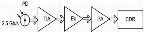
In an optical communication system, the optical receiver front-end is a key component in determining the dynamic range of the overall network. A photodetector, such as a photodiode (PD), and a high-speed TIA are the standard components of an optical receiver system. The current signal from the photodetector is amplified using a high-speed TIA [11, 12]. To ensure a consistent voltage signal that consistently oscillates at a suitable level for clock and data recovery, specific applications might require the installation of an additional high-gain broadband post-amplifier (PA) and equalizer, see Figure 2. To increase overall efficiency, the TIA measures the receiver's response and velocity. Therefore, to meet the needs of the optical receiver, it is essential to design a small-sized, low-power TIA employing CMOS technology. Here's a breakdown of TIAs: Here's a breakdown of TIA [12, 13]:
Figure 2. TIA is a standard front-end block diagram for an optical receiver
Both the decrease in mobility caused by the normal field and the limitation in velocity related to MOS devices will be ignored for simplicity. MOSFET equations for drain current and conductivity are based on the parasitic capacitance and the ratio of the width to the length of the conductor between the source and the drain, taking into account the effect of voltage as shown in the Eqs. (1)-(3) [28]:
$I_D=\frac{\mu_{n . p} C_{\mathrm{ox}}}{2}\left(\frac{W}{L}\right) V_{\mathrm{eff}}^2$ (1)
$g_m=\sqrt{2 \mu_{n . p} C_{\mathrm{ox}}\left(\frac{W}{L}\right) I_D}$ (2)
$g_m=\frac{2 I_D}{V_{\text {eff }}}$ (3)
where, $V_{\mathrm{eff}}=V_{G S}-V_{t n}$ for nMOS and $V_{\mathrm{eff}}=V_{S G}-\left|V_{t p}\right|$ for PMOS will be used throughout the paper. For bulk MOSFETs at room temperature, strong inversion often necessitates effective voltages (V "eff") above around 200 to 250mV.
The conductive substrate is eliminated in SOI chips. Although they have unique pathologies of their own, they can achieve reduced parasitic capacitance and better subthreshold slopes, which can result in lower power and/or higher speed [29].
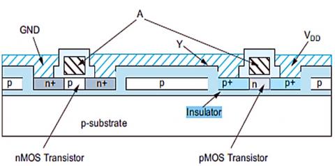
CMOS technology is being used more and more in ultra-low power systems like remote sensors that harvest energy from the environment and implantable medical devices that must operate for years on a tiny battery. At the cost of multiple orders of magnitude decrease in performance [30, 31], static CMOS gates functioning in the subthreshold regime can reduce the energy consumed per operation by an order of magnitude. Although SOI technology has long been the focus of research, it only gained commercial traction in 1998 when IBM began using it for PowerPC microprocessors. Although SOI has the potential to have reduced power consumption and higher performance [32], it also has certain odd transistor behavior that makes circuit design more difficult to handle and increases the cost of production. A cross-section of an inverter in an SOI process is shown in Figure 3 [33].
Benefits of SOI in CMOS optical amplifiers [30, 34]:
Figure 3. SOI inverter cross-section
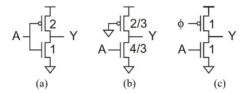
By substituting a single resistive pull-up for each of the pMOS transistors linked to the inputs, matched circuits lower the input capacitance [30]. Rationalized circuits have several disadvantages, including nonzero VOL, static power consumption, sluggish rising transitions, and contention over falling transitions. Dynamic circuits avoid these problems by utilizing a timed pull-up transistor in place of an always-on pMOS. A comparison of (a) static CMOS, (b) pseudo-nMOS, and (c) dynamic inverters is shown in Figure 4.
Since the clock Ǿ is zero during precharge, the clocked PMOS is ON and sets the output Y high. The clock is set to 1 and the clocked pMOS is turned off during evaluation. The output could be low or stay high [35]. Dynamic CMOS amplifiers benefit [30]:
Figure 4. Comparison of (a) static CMOS, (b) pseudo-nMOS, and (c) dynamic inverters
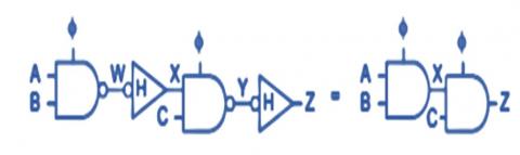
Certain functions, like XOR gates, need inversion by necessity, whereas domino gates are by nature noninverting [29]. This problem can be solved in three ways: by employing dual-rail domino logic, by delaying clocks, and by forcing inversions into static logic [31]. A traditional static CMOS XOR gate driven by the last domino circuit can be used to construct the required XOR gate at the end of the path in various circuits, including arithmetic logic units (ALUs). But now that it isn't rising monotonically, the XOR output can't trigger additional domino logic directly. To guarantee that the inputs are monotonic during evaluation, a second method involves directly cascading dynamic gates in place of the static CMOS inverter. This involves delaying the clock to the subsequent gates [32]. This is frequently implemented in NOR-NOR PLAs and content-addressable memory (CAMs). Figure 5. displays the symbols for the HI-skew inverter, domino AND, and dynamic NAND.
Figure 5. Domino gates
Over the course of a big chip, VDD and GND vary. Both are vulnerable to di/dt noise and IR drop-induced power supply noise [34]. As seen in Figure 6, IR drops happen between the supply pins and a block, drawing a current I across the resistance R of the power supply grid. When the current fluctuates quickly, di/dt noise develops across the power supply's inductance L. In particular, di/dt noise can be significant for blocks that are idle for multiple cycles [30]. There are design and layout techniques to mitigate power supply noise in CMOS amplifiers:
Figure 6. Power supply IR drops
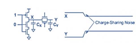
A transmission gate is driven by a dynamic inverter, as seen in Figure 7. Assume that the output is floating high due to the precharge of the dynamic gate. Assume further that Y = 0, and the transmission gate is off [29]. Charge sharing between X and Y will occur if the transmission gate is activated, disrupting the dynamic output.
Figure 7. On a dynamic gate-driven pass transistor charge
Power and ground wires inside the cells, as well as additional wires joining the cells together, make up the on-chip power distribution network [29]. Most cells have internal ground and power buses that are routed via either metal (1) or metal (2). To provide superior electro-migration immunity and reduced resistance, these wires are usually wider than the minimum. For instance, eight metal (1), power/ground buses are used by the cells on the inner front cover. Usually, an abutment connects these wires between neighboring cells. Rows of cells sharing common ground and power connections can be used in both standard cell designs and data paths [30].
These rows can be fastened together with even broader vertical metal wires in a compact, low-power form. An abstract diagram of this strapping is shown in Figure 8 (a). Figure 8 (b) displayed a typical cell layout fastened with [33].
Figure 8. Power allocation in a typical cell configuration
The design parameters of the op-amp in Figure 1 are obtained from the procedure proposed in Table 1 and meet all specifications, unlike the op-amp designed with different parameters. This study demonstrates that by utilizing this method, the compensation capacitor $C_c$ using Eq. (4) can be significantly reduced compared to other methods. The designer has more latitude to optimize the op-amp in terms of noise and power by picking from a wider variety of options.
Table 1. Parameter setting for the system proposed
|
Design Parameter |
Proposed |
|
$A_o$ (dB) |
80 |
|
$f_u$ (MHz) |
5.8 |
|
$\phi_M$ (deg) |
69 |
|
$S R$ (V/$\mu$sec) |
5.37/-5.36 |
|
Input-referred noise |
$\frac{20 \mathrm{nV}}{\sqrt{\mathrm{Hz}}}$ |
|
Cc (pf) |
0.393 |
|
Rc (kOhm) |
330.582 |
|
Ibias (uA) |
1.966 |
|
Total area (μm2) |
1220 |
|
ID (μA) |
15.35 |
|
Temperature (℃) |
300 |
|
Process transconductances |
kn=175e-8; kp=38.5e-7 |
|
Oxide thickness |
t_ox=9.6e-9 |
|
Vth |
Vtn=0.710; Vtp=-0.901 |
$C_c=\frac{16 T k}{3 \omega_u S_n(f)}\left[2+\frac{R S}{\omega_u\left(V_{\mathrm{HR}}^{C M+}+V_{t n}\right)}\right]$ (4)
Eq. (5) can be used to control the current. By adjusting various parameters, the designer can achieve greater control over the op-amp's power and noise characteristics.
$I_{D(a l l)}=R S\left(C_c+C_L\right)$ (5)
Channel length for CMOS to enhance delay of switching and current, Eq. (6) refers to channel length.
$\mathrm{W}=\frac{2 S R\left(C_c+C_L\right)}{\mu_p C_{\mathrm{ox}}\left(V_{\mathrm{HR}}^{\text {out+ }}\right)^2} L$ (6)
The current can be managed with the use of Eq. (7). The power and noise characteristics of the op-amp can be more precisely controlled by the designer by varying the W/L of several factors.
$\left(\frac{W}{L}\right)=\frac{2 C_c S R}{\mu_p C_{\mathrm{ox}} V_{\mathrm{HR}}^{\text {out+}}\left(V_{\mathrm{DD}}-V_{\mathrm{HR}}^{\text {out+ }}-2\left|V_{t p}\right|\right)}$ (7)
The circuit was created to satisfy the requirements listed in Tables 2-4, which show that for positive slews, M1 moves into the cut-off region as Vin+ rises. This indicates that M2 receives all of the current from M0. This transistor will enter the deep linear zone if the gate of M2 is subjected to an extremely high voltage. As a result, M2’s drain-source voltage will significantly decrease, leaving M5’s gate voltage extremely low. This results in an extremely low M5 gate voltage, which indicates a high overdrive voltage for this transistor. As a result, M5 operates within a deep linear range, thereby raising the output voltage to approximately the same level. Table 2 represents the calculation of Mosfet size with drain current and power consumption when the load capacitor CL equals 5pF.
Table 2. The results system for load capacitor CL equals 5pF
|
MOSFET Sizing |
||||
|
|
W (nm) |
L (nm) |
S (nm/nm) |
|
|
M1 |
516.069 |
1000.000 |
0.516 |
|
|
M2 |
516.069 |
1000.000 |
0.516 |
|
|
M3 |
28.035 |
1000.000 |
0.028 |
|
|
M4 |
28.035 |
1000.000 |
0.028 |
|
|
M5 |
19.424 |
1000.000 |
0.019 |
|
|
M6 |
0.000 |
0.000 |
0.769 |
|
|
M7 |
266.399 |
1000.000 |
0.266 |
|
|
M8 |
19.424 |
1000.000 |
0.019 |
|
|
Drain Current |
||||
|
|
I (uA) |
Power Consumption (uW) |
||
|
I1 |
0.983 |
P = 55.618 |
||
|
I2 |
0.983 |
|||
|
I3 |
0.983 |
|||
|
I4 |
0.983 |
|||
|
I5 |
1.966 |
|||
|
I6 |
26.966 |
|||
|
I7 |
26.966 |
|||
|
I8 |
1.966 |
|||
Table 3. The results system for load capacitor CL equals 1pF
|
MOSFET Sizing |
||||
|
|
W (nm) |
L (nm) |
S (nm/nm) |
|
|
M1 |
411.897 |
1000.000 |
0.412 |
|
|
M2 |
411.897 |
1000.000 |
0.412 |
|
|
M3 |
26.261 |
1000.000 |
0.026 |
|
|
M4 |
26.261 |
1000.000 |
0.026 |
|
|
M5 |
18.921 |
1000.000 |
0.019 |
|
|
M6 |
0.000 |
0.000 |
0.220 |
|
|
M7 |
79.206 |
1000.000 |
0.079 |
|
|
M8 |
18.921 |
1000.000 |
0.019 |
|
|
Drain Current |
||||
|
|
I (uA) |
Power Consumption (uW) |
||
|
I1 |
0.785 |
P = 19.416 |
||
|
I2 |
0.785 |
|||
|
I3 |
0.785 |
|||
|
I4 |
0.785 |
|||
|
I5 |
1.569 |
|||
|
I6 |
6.569 |
|||
|
I7 |
6.569 |
|||
|
I8 |
1.569 |
|||
Table 4. The results system for load capacitor CL equals 0.5pF
|
MOSFET Sizing |
||||
|
|
W (nm) |
L (nm) |
S (nm/nm) |
|
|
M1 |
411.897 |
1000.000 |
0.412 |
|
|
M2 |
411.897 |
1000.000 |
0.412 |
|
|
M3 |
26.261 |
1000.000 |
0.026 |
|
|
M4 |
26.261 |
1000.000 |
0.026 |
|
|
M5 |
18.921 |
1000.000 |
0.019 |
|
|
M6 |
0.000 |
0.000 |
0.136 |
|
|
M7 |
49.064 |
1000.000 |
0.049 |
|
|
M8 |
18.921 |
1000.000 |
0.019 |
|
|
Drain Current |
||||
|
|
I (uA) |
Power Consumption (uW) |
||
|
I1 |
0.785 |
P = 14.416 |
||
|
I2 |
0.785 |
|||
|
I3 |
0.785 |
|||
|
I4 |
0.785 |
|||
|
I5 |
1.569 |
|||
|
I6 |
4.069 |
|||
|
I7 |
4.069 |
|||
|
I8 |
1.569 |
|||
The Mosfet size calculation with drain current and power consumption, when the load capacitor CL equals 1 pF, is shown in Table 3. The table indicates that lowering the load capacitance will lower the power consumed, currents, and other significant variables.
Table 4 displays the computation of the Mosfet size with drain current and power consumption when the load capacitor CL = 0.5 pF. According to the table, reducing the load capacitance will result in a decrease in power consumption, currents, and other important factors.
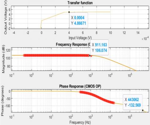
Figure 9 show the response (transfer function frequency response and phase response) for CMOS, the magnitude equals 110 dB when 1 kHz). These figures explain the behavior of the two-stage CMOS op-amp response.
Figure 9. Two-stage CMOS op-amps (transfer function frequency response and phase response)
The process of calculating the numbers in Tables 2-4 is a simulation process using MATLAB, where the equations of the programmatically designed system were applied and the values were calculated through simulations built on the basis of the equations.
The improvements in CMOS technology in this study aim to reduce power and noise levels as well as currents in a two-stage low-noise CMOS op-amp circuit. Reducing power consumption and currents results in lower losses as well as higher-quality signals in applications such as precision instruments, communication receivers, and professional audio equipment. Achieving low performance often means increasing the rate of packets to be sent. The overall performance should be ideal for low-noise amplifiers, where the noise level, power consumed, and low currents are the most important features from an application perspective. Therefore, improving the performance of operational amplifiers requires a sound design strategy.
Suggestions for future studies include increasing the number of stages, reducing the width to length, and also using improved feedback for the design.
|
Im |
Maximum current |
|
S |
Slew rate |
|
Vm |
Maximum voltage |
|
Pm |
Maximum power |
|
G |
Gain |
|
IC |
Drain current |
|
Is |
Saturation current |
[1] Zhang, J., Zhuo, W., Ma, C. (2023). A CMOS transimpedance amplifier with broad-band and high gain based on negative Miller capacitance. Integration, 91: 60-66. https://doi.org/10.1016/j.vlsi.2023.03.004
[2] Niranjan, V., Jhamb, M. (2023). Design of a low-power 180 nm broadband CMOS transimpedance amplifier for bio-medical & IoT applications. International Journal of Information Technology, 15(5): 2741-2745. https://doi.org/10.1007/s41870-023-01315-6.
[3] Takahashi, Y., Ito, D., Namamura, M., Tsuchiya, A., Inoue, T., Kishine, K. (2022). Low-power regulated cascode CMOS transimpedance amplifier with local feedback circuit. Electronics, 11(6): 854. https://doi.org/10.3390/electronics11060854
[4] Yeom, J.H., Park, K., Choi, J., Song, M., Kim, S.Y. (2019). Low-cost and high-integration optical time domain reflectometer using CMOS technology. In Conference on Ph.D Research in Microelectronics and Electronics (PRIME), Lausanne, Switzerland, pp. 145-148. https://doi.org/10.1109/prime.2019.8787845
[5] Gupta, S. (2008). Electronics Devices and Circuits. New Delhi: Dhanpat Rai Publications.
[6] Geiger, R.L., Allen, P.E., Strader, N.R. (1990). VLSI design techniques for analog and digital circuits (Vol. 90). New York: McGraw-Hill.
[7] Aminzadeh, H., Lotfi, R. (2007). Design guidelines for high-speed two-stage CMOS operational amplifiers. Arabian Journal for Science and Engineering, 32(2): 76-88.
[8] Allen, P.E., Holberg, D.R. (2002). CMOS Analog Circuit Design. New York: Oxford University Press.
[9] Palmisano, G., Palumbo, G., Pennisi, S. (2001). Design procedure for two-stage CMOS transconductance operational amplifiers: A tutorial. Analog Integrated Circuits and Signal Processing, 27: 179-189. https://doi.org/10.1023/A:1011229119071
[10] Gray, P.R., Hurst, P.J., Lewis, S.H., Meyer, R.G. (2009). Analysis and Design of Analog Integrated Circuits. John Wiley & Sons.
[11] Johns, D.A., Martin, K. (1997). Analog Integrated Circuit Design. Toronto: University of Toronto Press.
[12] Montgomery, D.C. (1997). Design and Analysis of Experiments (4th ed.). New York: John Wiley & Sons.
[13] CMOS and Design Procedure for Two-Stage CMOS Opamp. (2018). Retrieved from https://graduateway.com/cmos-and-design-procedure-for-two-stage-cmos-opamp.
[14] Baker, R.J., Li, H.W., Boyce, D.E. (1998). CMOS Circuit Design, Layout, and Simulation. New York: Wiley Interscience.
[15] Dahigaonkar, D.J., Wakde, D.G., Khare, A. (2014). A low voltage Wideband CMOS operational transconductance amplifier for VHF applications. In 2014 International Conference on Electronic Systems, Signal Processing and Computing Technologies, Nagpur, India, pp. 89-92. https://doi.org/10.1109/ICESC.2014.95
[16] Panda, B., Dash, S.K., Mishra, S.N. (2014). High slew rate op-amp design for low power applications. In 2014 International Conference on Control, Instrumentation, Communication and Computational Technologies (ICCICCT), Kanyakumari, India, pp. 1096-1100. https://doi.org/10.1109/iccicct.2014.6993124
[17] Akbari, M., Biabanifard, S., Hashemipour, O. (2014). Design of ultra-low-power CMOS amplifiers based on flicker noise reduction. In 2014 22nd Iranian Conference on Electrical Engineering (ICEE), Tehran, Iran, pp. 403-406. https://doi.org/10.1109/iraniancee.2014.6999573
[18] Ranjan, R. (2016). Design of low power operational amplifier and digital latch circuits using power efficient charge steering technique. In 2016 IEEE International Conference on Recent Trends in Electronics, Information & Communication Technology (RTEICT), Bangalore, India, pp. 316-321. https://doi.org/10.1109/RTEICT.2016.7807834
[19] Raghuveer, V., Balasubramanian, K., Sudhakar, S. (2017). A 2μV low offset, 130 dB high gain continuous auto zero operational amplifier. In 2017 International Conference on Communication and Signal Processing (ICCSP), Chennai, India, pp. 1715-1718. https://doi.org/10.1109/ICCSP.2017.8286685
[20] Mai, T., Schmid, K., Röber, J., Hagelauer, A., Weigel, R. (2017). A fully-differential operational amplifier using a new chopping technique and low-voltage input devices. In 2017 24th IEEE International Conference on Electronics, Circuits and Systems (ICECS), Batumi, Georgia, pp. 74-77. https://doi.org/10.1109/ICECS.2017.8292081
[21] Faheem, A., Bhagat, N., Khot, U.P. (2018). Design of low voltage supply current feedback operational amplifier. In 2018 Second International Conference on Inventive Communication and Computational Technologies (ICICCT), Coimbatore, India, pp. 1713-1716. https://doi.org/10.1109/ICICCT.2018.8473056
[22] Parthipan, A., Krishna, K.L., Kumar, V.N., Hareesh, C., Raviteja, B., Varshath, C.V. (2019). A high performance CMOS operational amplifier. In 2019 3rd International Conference on Computing Methodologies and Communication (ICCMC), Erode, India, pp. 702-706. https://doi.org/10.1109/ICCMC.2019.8819641
[23] Srivastava, S., Sharma, T. (2019). Performance analysis of operational amplifier for high gain & low power applications. In 2019 4th International Conference on Information Systems and Computer Networks (ISCON), Mathura, India, pp. 208-212. https://doi.org/10.1109/ISCON47742.2019.9036199
[24] Maia, N.J., Sanchez, A.R., Moreno, R.L., Pimenta, T.C., Ferreira, L.H.C. (2020). A low power CMOS operational transconductance amplifier with improved CMRR. In 2020 32nd International Conference on Microelectronics (ICM), Aqaba, Jordan, pp. 1-4. https://doi.org/10.1109/ICM50269.2020.9331501
[25] Al-Hashimi, J., Abugharbieh, K. (2021). Design of a switched-mode operational amplifier operating with a 0.5 V supply voltage. In 2021 19th IEEE International New Circuits and Systems Conference (NEWCAS), Toulon, France, pp. 1-4. https://doi.org/10.1109/NEWCAS50681.2021.9462733
[26] Dehkordi, M.A., Mirsanei, S.M., Zohoori, S. (2021). A CMOS low-noise and low-power transimpedance amplifier. In 2021 29th Iranian Conference on Electrical Engineering (ICEE), Tehran, Iran, Islamic Republic of, pp. 107-111. https://doi.org/10.1109/ICEE52715.2021.9544118
[27] Surabhi, S.P. (2022). Design and analysis of low power high gain amplifiers for DAC application. In 2022 IEEE International Conference on Data Science and Information System (ICDSIS), Hassan, India, pp. 1-6. https://doi.org/10.1109/ICDSIS55133.2022.9915853
[28] Stancu, C., Dobrescu, D., Dobrescu, L. (2022). Offset voltage reduction methods for a two-stage folded cascode operational amplifier. In 2022 14th International Conference on Electronics, Computers and Artificial Intelligence (ECAI), Ploiesti, Romania, pp. 1-4. https://doi.org/10.1109/ECAI54874.2022.9847308
[29] Razavi, B. (2016). Design of Analog CMOS Integrated Circuits. McGraw-Hill.
[30] Weste, N.H., Harris, D. (2015). CMOS VLSI design: A circuits and systems perspective. Pearson Education India. http://ci.nii.ac.jp/ncid/BA67993239.
[31] Lin, M. (2011). Introduction to VLSI Systems: A logic, Circuit, and System Perspective. CRC Press. https://doi.org/10.1201/9781439897324
[32] Kerns, S., Massengill, L., Kerns, D., Alles, M.L., Houston, T., Lu, H., Hite, L. (1989). Model for CMOS/SOI single-event vulnerability. IEEE Transactions on Nuclear Science, 36(6): 2305-2310. https://doi.org/10.1109/23.45440
[33] Inac, O., Uzunkol, M., Rebeiz, G.M. (2014). 45-Nm CMOS SOI Technology characterization for Millimeter-Wave applications. IEEE Transactions on Microwave Theory and Techniques, 62(6): 1301-1311. https://doi.org/10.1109/tmtt.2014.2317551
[34] Gitelman, L., Stolyarova, S., Bar-Lev, S., Gutman, Z., Ochana, Y., Nemirovsky, Y. (2009). CMOS-SOI-MEMS transistor for uncooled IR imaging. IEEE Transactions on Electron Devices, 56(9): 1935-1942. https://doi.org/10.1109/ted.2009.2026523
[35] Ding, L., Mazumder, P. (2004). On circuit techniques to improve noise immunity of CMOS dynamic logic. IEEE Transactions on Very Large Scale Integration (VLSI) Systems, 12(9): 910-925. https://doi.org/10.1109/tvlsi.2004.833668