Abbas Ghayebloo* | Mohsen Ghaleghovand | Abolfazl Jalilvand
© 2021 IIETA. This article is published by IIETA and is licensed under the CC BY 4.0 license (http://creativecommons.org/licenses/by/4.0/).
OPEN ACCESS
In this paper, a new controller design approach for DC-DC flyback converter has been proposed and compared with classic controller design approach. The proposed controller design method has been innovated from the identification LS method that previously applied on parameter identification. The proposed method exchanges the controller design problem to the identification problem. The proposed approach has two considerable superiority compared with common methods. It can design a controller with the desired structure and desired performance. Regard to these advantages, it can be notated that the proposed approach is well suited for SMPS application where benefits from analog controllers for the decreased total cost. For controller design purposes, the large and small-signal models of the flyback converter, using well-known state-space averaging and linearization methods have been extracted and controllers with classic and proposed approaches have been designed. Also, it proved that the conventional peak current controller used in commercial current-mode analog controllers is equivalent to a proportional average controller. One practical flyback converter has designed and implemented in continuous mode with two controllers and some experimental and simulation results have been provided for verification of the proposed method. The simulation and experimental results show that the proposed design approach can provide a controller with the desired structure and performance.
controller design, identification approach, least squares method, flyback converter
DC power supplies have two linear and switching types. Linear power supplies have some advantages compared to switching power supplies such as simple design, high stability, low noise, fast response time and low output ripple but they have some more important disadvantages such as low efficiency, low power per volume and weight and low voltage capabilities. The switching power supplies have low power loss because their switching elements work only in on or off states. Also, they have lower volume and weight per power unit because they work with the very high switching frequency, compared by linear types that work with low grid frequency. Furthermore, with ever-increasing developments in voltage and current ratings, switching frequency and cost decreasing of semiconductor devices, switching power supplies are being dominated [1].
Switching power supplies have two isolated and non-isolated types. Among the isolated switching power supplies, the flyback converter has been utilized as the power supply of various electronic systems, because of its simple structure [2]. It has very high utilization gain in power ratings under 200 W. Almost power supplies of all cell-phones, laptops, PCs, monitoring equipment, medical equipment and so on are flyback converter [3]. The main reason of the high usage of this converter is its high reliability, high efficiency and low cost because it has only one switching element. This converter operates as a step-up or step-down converter [4].
Flyback converter can work with fixed and variable switching frequency. A small-signal modelling of flyback with variable frequency has been proposed by Chen et al. [5]. In this work common operation of this converter i.e., fixed-frequency operation has not been utilized.
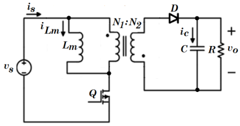
Figure 1 shows the simple structure of the flyback converter. It consists of one switching transistor on the primary side of the isolation transformer which connected to the input voltage and one diode and one capacitor which connected to load on the secondary side. In continuous conduction mode, this converter has two switching states. In the first state, the transistor is on and the diode is off therefore the magnetizing inductance of the transformer would be energized by the input voltage and in the second state of the switching interval, the switch in off and the diode is on therefore the energy of the magnetizing inductance will be transferred to load.
Figure 1. The simple structure of flyback converter
Common controllers for switching power supplies are classic controllers such as proportional-integral controller, one zero-one pole controller, one pole controller and so on that they implemented by analog integrated circuits. Industrial analog ICs for implementing the controllers for switching power supplies are offered by manufacturers in two types so called voltage mode and current mode controllers. The voltage mode controllers have been reviewed by Bogdan and Bizon [6] and current control mode controllers have discussed by Wan [7]. In current mode ICs, beside of outer voltage control loop, there exists an inner current control loop. The inner current control loop increases the stability of the control loop and it is appreciated for non-minimum phase converters with unstable zero such as flyback converter. A new analog IC structure for constant current control of flyback converter has been proposed by Li and Zhu [8].
It is common that to design a controller for SMPSs, a classic approach based on much-approximated models of them i.e., just poles and zeros related to output filter and capacitor and so on has been used. In this simple approach, the controller zeros or poles have been placed on model approximated poles and zeros and the more accurate models such as state-space averaging models be not utilized. Therefore, in these approaches desired performance such as overshoot or settling time cannot be applied in the controller design procedure. The analog implementation of these controllers using analog SMPS controller chips for low-cost applications, constrain the structure of these controllers.
Such controllers must be selected among a few structures such as one pole, one pole with the limited band, one pole-one zero, two pole-two zero and so on and any controller suggested by many methods such as nonlinear sliding mode [9-11] and fuzzy [12] could not be used.
This paper aims to propose a novel controller design that benefits two main advantages: the desired structure with the desired performance as much as possible. The proposed method is based on least square parameter identification method and can exchange a controller design problem to the identification problem. This idea in the authors view has high novelty and opens a new viewpoint in controller design using various and sophisticated identification methods. This idea can be developed to using from observers design methods, filters design methods and optimization methods for controller design and vice versa because in all controller, observer, filter, identification and optimization design methods, mathematically an error must be minimized.
The proposed approach has been applied to flyback as an example. It must be noted that this approach is completely general and can be applied on other SMPSs that benefit from analog controllers or other systems with classic controllers.
The remainder of this paper has been organized as follows. In section 2, a flyback converter has been designed based on some input design parameters. For designed converter classic one pole with the limited band and one pole-one zero controllers have been designed using the classic method. The state-space model and the linearized small-signal model of flyback converter and controllers models have been reported in section 3. These models will be used for the proposed controller design in subsequent sections. In section 4, the proposed approach will be presented. The classic and proposed controller simulation and experimental results have been provided in section 5. Finally, some conclusions have prepared in section 6.
The design input parameters for an isolated power supply for the target inverter driver board have depicted in Table 1. In this design, the continuous conduction mode has been selected. Conduction mode type (continuous or discontinuous) is an important design parameter that can affect the converter in various aspects such as dynamics, ripple of output voltage, stress on switching devices, primary and secondary peak currents and isolation transformer size.
Table 1. The flyback design input parameters
|
Parameter |
Value |
|
Input voltage |
24±10% ac |
|
Output voltage |
12 Volts |
|
Maximum output ripple |
1% |
|
Rated power |
5 W |
|
Minimum efficiency |
70% |
|
Switching frequency |
60 kHz |
|
Maximum core flux density |
0.3 Tesla |
Discontinuous conduction mode has a fast response to variation of input voltage and output current because it has not unstable zero compared to continuous conduction mode. This unstable zero appears in converters models witch in switch off state mode, the output capacitor supplies the load current alone. Despite this advantage, the discontinuous conduction mode has some drawbacks such as high peak current, higher rating values of the switch, diode and output filter, more nonlinearity and higher EMI.
2.1 Power circuit design
For the power circuit design of the desired converter, the detailed classic design procedure for electric and magnetic design in the researches [13, 14] has been utilized and finally, the parameters in Table 2, have been resulted.
Table 2. The power circuit parameters of designed flyback
|
Parameter |
Value |
|
Rated duty cycle |
33% |
|
Core Type |
ETD-29 |
|
Wire diameter |
0.45 mm |
|
Input rectifier capacitor (10% ripple) |
650 μF |
|
Primary turn number |
161 |
|
Secondary turn number |
120 |
|
Total air gap length |
1.95 mm |
|
Transformer magnetizing inductance (Primary side) |
1.9 mH |
|
Power Switch |
IRF840 |
|
Output capacitor (50 mV ripple) |
220 μF |
|
Snubber type |
RCD |
|
Snubber capacitor |
10 nF |
2.2 Controller structure selection
As previously mentioned, the analog ICs for switching power supplies are offered by manufactures in two voltage mode and current mode types. The voltage mode controllers have some advantages such as simple design and analysis but they have some drawbacks such as low response time to the input voltage and output current variations, more complicated controller design and more dependency of their gain to input voltage. Compared to single loop voltage control mode, the current mode control ICs have an additional inner loop. In the inner loop, the current of the inductor has been sensed and utilized for duty cycle control. The current mode control has better load and line regulation and high stability. In this design, the UC3845 current-mode controller has been used for analog controller implementation.
Some analog controllers that can be implemented by standard ICs have suggested for power converters such as single-pole compensator, single-pole with limited band compensator, one pole-one zero compensator and two poles- two zeros compensator. Among these compensators, limited band single pole and one pole-one zero compensators have been suggested for the current mode flyback converter. The performance of the mentioned converters in the aspect of transient response and load regulation is depicted in Table 3. It must be noted that compensators beside of their poles and zeros have one ideal or limited band integrator to eliminate the steady-state error of the output voltage.
Table 3. The performance of various analog compensators [13]
|
Compensator |
Line regulation |
Transient response |
|
Single pole |
good |
Weak |
|
Single pole with limited band |
average |
Good |
|
One pole-one zero |
good |
Good |
|
Two poles-two zeros |
good |
Good |
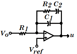
The structure of one pole-one zero compensator is shown in Figure 2. This compensator has a pole in origin caused a high DC gain for good regulation of output voltage. By designing the zero corner frequency of controller below the output filter pole, the leading phase of that compensate the delay caused by the output filter pole. Also, the pole of the compensator can be placed on the output capacitor equivalent series resistance (ERS) zero to eliminate its effect by decreasing gain gradually.
Figure 2. The one pole-one zero compensator structure
The structure of the limited band single-pole compensator is similar to one pole-one zero compensator. The only difference is the series capacitor with R2 i.e., C2 does not exist in its structure. The circuit elements of these controllers will be designed by classic approach in the next subsection and by proposed identification approach in section 4.
2.3 Controllers circuit design with the classic approach
For controllers design, at first, classic approach has been used. Generally, for controller design purposes, the system transfer function from controller output (error amplifier output) to output voltage is needed. In classic approaches that are commonly used, instead of an accurate transfer function, the approximated zeros, poles and DC gain of the converter are used for controller design. In these design procedures, the DC gain, output filter pole corner frequency and output capacitor ESR zero corner frequency of flyback converter can be calculated as Eqns. (1)-(3) [13].
$\mathrm{A}=\frac{\left(V_{s}-\mathrm{V}_{o}\right)^{2}}{V_{s} \times \Delta V_{e}} \times \frac{N_{2}}{N_{1}}$ (1)
$f_{p}=1 /(2 \pi R C)$ (2)
$f_{E S R}=1 /\left(2 \pi R_{E S R} C\right)$ (3)
Where for current mode controllers, ∆Ve is the voltage related to maximum current (for UC3845 is 1 volt). Most of capacitor manufactures do not report the ESR value for their products. Typically, the corner frequency of ESR zero for electrolyte capacitors has a value between 1 kHz to 5 kHz.
The corner frequency of pole and DC gain of the single-pole with limited band compensator can be calculated according to Eqns. (4)-(5).
${{\text{f}}_{\text{pc}}}\text{=1/(}2\pi {{R}_{2}}{{C}_{1}}\text{)}$ (4)
${{\text{A}}_{c}}\text{=}{{\text{R}}_{\text{2}}}\text{/}{{R}_{1}}$ (5)
Also, the corner frequencies of one pole-one zero compensator zero and pole and its DC gain can be calculated according to Eqns. (6)-(8).
${{\text{f}}_{\text{zc}}}\text{=1/(}2\pi {{R}_{2}}{{C}_{2}}\text{)}$ (6)
${{\text{f}}_{\text{pc}}}\text{=(}{{C}_{1}}+{{C}_{2}})/(2\pi {{R}_{2}}{{C}_{1}}{{C}_{2}})$ (7)
${{A}_{c}}\text{=1/(}{{R}_{1}}{{C}_{1}}+{{R}_{1}}{{C}_{2}})$ (8)
Before compensator design, at first, the converter frequency domain parameters such as open-loop DC gain (control to output) and the corner frequencies of output filter pole and output capacitance zero must be calculated. The open-loop DC gain of converter obtained 9.45 (19.5 dB). Also, the corner frequencies of output filter for light (50% nominal) and nominal load can be obtained 13 Hz and 26 Hz respectively. In this design, the corner frequency of capacitance ESR has been considered equal to 2 kHz.
For compensator design with the classic approach, the cutting frequency of the converter-controller closed-loop transfer function can be considered one-sixth of switching frequency to eliminate the switching ripples in the control loop. For switching frequency of 60 kHz, the closed-loop cutting frequency (fcl) can be considered less than or equal to 10 kHz. The amount of extra gain to rise up the control to output gain diagram for achieving to desired closed-loop cutting frequency can be obtained from Eqns. (9)-(10). This extra gain must be calculated for the worst case i.e., nominal load (fp).
${{G}_{\text{ex}}}\text{=}20Log\text{(}{{\text{f}}_{cl}}\text{/}{{\text{f}}_{\text{p}}}\text{)-A}=32.2dB$ (9)
${{A}_{ex}}\text{=1}{{\text{0}}^{\text{(}{{\text{G}}_{\text{ex}}}/20\text{)}}}=40.7$ (10)
In the classic design approach, for band limited single-pole compensator design with the classic approach, commonly, its pole is locating on ESR zero and for one pole-one zero compensator, the compensator zero is locating on the pole of the output filter with the least real value i.e., light load pole and its pole is locating on ESR zero. After calculating the gain, zero and pole of two compensators, the values of circuit elements of them can be obtained as Table 4.
Table 4. The controller circuit parameters of designed flyback with classic approach
|
Compensator |
Elements |
Value |
|
Band limited single pole controller |
R1 |
10K||39K→7.95KΩ |
|
R2 |
330KΩ |
|
|
C1 |
240pF |
|
|
One pole-One zero controller |
R1 |
10K||39K→7.95KΩ |
|
C1 |
20nF |
|
|
C2 |
3.08µF |
|
|
R2 |
3.9KΩ |
State-space average modelling of switch-mode converters is a well-known and sophisticated approach for extracting model of converters and reported in literature such as [15-17].
According to Figure 1, in switch on state duration (0<t<dTs), the diode is off and the transformer magnetizing inductance will be charged by the input voltage and the capacitor in the output side will be discharged by the load and Eqns. (11)-(12) can be written.
$\frac{d{{i}_{Lm}}}{dt}=\frac{{{v}_{s}}}{{{L}_{m}}}$ (11)
$\frac{d{{v}_{o}}}{dt}=-\frac{{{v}_{o}}}{rC}$ (12)
In switch off-state duration (dTs<t<Ts: for continuous conduction mode), the diode is on therefore the transformer magnetizing inductance will be discharged by the referred output voltage to the transformer primary side and the capacitor will be charged by diode current and also discharged by the load.
$d{{i}_{Lm}}=-\frac{n{{v}_{o}}}{{{L}_{m}}}$ (13)
$\frac{d{{v}_{o}}}{dt}=-\frac{n{{i}_{Lm}}}{C}-\frac{{{v}_{o}}}{rC}$ (14)
where, n is the turn ratio of the primary to the secondary side of the transformer and Lm is the transformer magnetizing inductance, r is load resistance and d is the duty cycle of the switch. By applying the state-space averaging method to Eqns. (11)-(14) simply the large-signal state-space model of flyback converter can be derived according to Eq. (15). It is obvious that this converter has a nonlinear state-space model and needs nonlinear controllers such as SMC for increased performance.
$\left[ \begin{matrix} \frac{d{{i}_{Lm}}}{dt} \\ \frac{d{{v}_{o}}}{dt} \\\end{matrix} \right]=\left[ \begin{matrix} 0 & -\frac{n(1-d)}{{{L}_{m}}} \\ \frac{n(1-d)}{{{L}_{m}}} & -\frac{1}{rC} \\\end{matrix} \right]\left[ \begin{matrix} {{i}_{Lm}} \\ {{v}_{o}} \\\end{matrix} \right]+\left[ \begin{matrix} \frac{d\,{{v}_{s}}}{{{L}_{m}}} \\ 0 \\\end{matrix} \right]$ (15)
By linearizing the large-signal model of flyback converter about operating point by substituting the instantaneous values with the summation of DC and perturbed values for switch duty cycle ($d \rightarrow D+\tilde{d}$), input voltage ($v_{s} \rightarrow V_{s}+v_{s}$), output voltage ($v_{o} \rightarrow V_{o}+v_{o}$), magnetizing inductance current ($i_{L m} \rightarrow I_{L m}+i_{L m}$) and load resistance ($r \rightarrow R+\tilde{r}$) and ignoring the high order perturbed terms, the linear model of flyback converter can be derived according to Eq. (16). In this equation $\tilde{d}$ is control input but $\tilde{v_{s}}$ and $\tilde{r}$ are disturbance inputs. Since both of two system states are measured in closed loop system therefore system is fully observable. Also, controllability issue can be concluded because of non-zero values of the first column of B matrix in Eq. (16) for the control input.
$\left[ \begin{matrix} \frac{d\overset{\tilde{\ }}{\mathop{{{i}_{Lm}}}}\,}{dt} \\ \frac{d\overset{\tilde{\ }}{\mathop{{{v}_{o}}}}\,}{dt} \\\end{matrix} \right]=\left[ \begin{matrix} 0 & -\frac{n(1-D)}{{{L}_{m}}} \\ \frac{n(1-D)}{{{L}_{m}}} & -\frac{1}{RC} \\\end{matrix} \right]\left[ \begin{matrix} \overset{\tilde{\ }}{\mathop{{{i}_{Lm}}}}\, \\ \overset{\tilde{\ }}{\mathop{{{v}_{o}}}}\, \\\end{matrix} \right]+\left[ \begin{matrix} \frac{n{{V}_{o}}+{{V}_{s}}}{{{L}_{m}}} & \frac{D}{{{L}_{m}}} & 0 \\ -\frac{n{{I}_{Lm}}}{C} & 0 & \frac{{{V}_{o}}}{C{{R}^{2}}} \\\end{matrix} \right]\left[ \begin{matrix} \overset{\tilde{\ }}{\mathop{d}}\, \\ \begin{align} & \overset{\tilde{\ }}{\mathop{{{v}_{s}}}}\, \\ & \overset{\tilde{\ }}{\mathop{r}}\, \\ \end{align} \\\end{matrix} \right]$ (16)
Finally, with the output vector as same as the state vector, the transfer functions from the duty cycle to outputs can be calculated using state-space to transfer function relation and Eqns. (17) and (18) can be derived. As could be seen from denominators of Eqns. (17) and (18), all coefficients of 2nd order systems are positive therefore it is a BIBO stable system. But Eq. (18) has an unstable zero which must be handled by the controller.
$\frac{\overset{\tilde{\ }}{\mathop{{{i}_{Lm}}}}\,(s)}{\overset{\tilde{\ }}{\mathop{d}}\,(s)}=\frac{CR(n{{V}_{o}}+{{V}_{s}})s+(n{{V}_{o}}+{{V}_{s}})+R{{n}^{2}}{{(1-D)}^{2}}{{I}_{Lm}}}{{{L}_{m}}CR{{s}^{2}}+{{L}_{m}}s+R{{n}^{2}}{{(1-D)}^{2}}}$ (17)
$\frac{\overset{\tilde{\ }}{\mathop{{{v}_{o}}}}\,(s)}{\overset{\tilde{\ }}{\mathop{d}}\,(s)}=\frac{-n{{L}_{m}}R{{I}_{Lm}}s+Rn(1-D)(n{{V}_{o}}+{{V}_{s}})}{{{L}_{m}}CR{{s}^{2}}+{{L}_{m}}s+R{{n}^{2}}{{(1-D)}^{2}}}$ (18)
It is obvious that the derived model is more accurate compared to the classic approximate model. It has an additional stable pole and one unstable zero and will be used for controller design. As can be seen from Eq. (18), the transfer function from the duty cycle to output voltage is non-minimum phase.
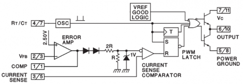
Figure 3 shows the schematic of the controller section of UC3845 chip. As it can be seen from this figure, the PWM latch has been reset lead to reset the output pulse when the increasing magnetizing inductance current in switch on mode (pin 3/5) reaches the one-third of error amplifier output. This means this section controls the peak current of magnetizing inductance with an on/off controller.
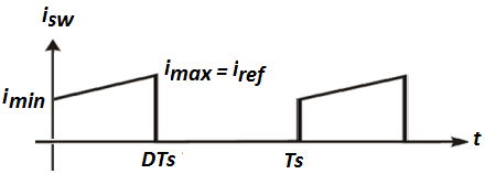
Now we can prove that the mentioned on/off control of magnetizing current peak is equivalent with a proportional controller that controls magnetizing average value. Figure 4 shows one of the well-known key waveforms of the flyback converter in continuous conduction mode. As it can be seen from this figure, the power switch current in on-mode, increases monolithically with slope Vin/Lm. Using Figure 4, Eqns. (19)-(20) can be written and with substituting imin Eq. (21) can be derived.
$\frac{{{\text{i}}_{\text{ref}}}-{{i}_{\min }}}{d{{T}_{s}}}\text{=}\frac{{{v}_{s}}}{{{L}_{m}}}$ (19)
${{\text{i}}_{\text{Lm}}}\text{=}\frac{{{i}_{ref}}+{{i}_{\min }}}{2}$ (20)
$\text{d=}\frac{2{{L}_{m}}}{{{T}_{s}}{{v}_{s}}}({{i}_{ref}}-{{i}_{Lm}})$ (21)
Eq. (21) proves that the current loop in UC3845 and many SMPS analog controllers are proportional controllers. By simple circuit theory manipulations, the transfer functions of limited band single-pole controller and one pole-one zero controller, depicted in Figure 2 can be derived as Eqns. (22)-(23) respectively.
${{G}_{c}}=\frac{{{d}_{0}}}{s+{{c}_{0}}}=\frac{(1/{{R}_{1}}{{C}_{2}})}{s+(1/{{R}_{2}}{{C}_{2}})}$ (22)
${{G}_{c}}=\frac{{{d}_{1}}s+{{d}_{0}}}{{{s}^{2}}+{{c}_{1}}s}=\frac{\frac{1}{{{R}_{2}}{{C}_{2}}}s+\frac{1}{{{R}_{1}}{{R}_{2}}{{C}_{1}}{{C}_{2}}}}{{{s}^{2}}+\frac{{{C}_{1}}+{{C}_{2}}}{{{R}_{2}}{{C}_{1}}{{C}_{2}}}s}$ (23)
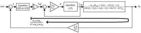
Using derived transfer functions for the converter, current loop controller and voltage loop controller, the block diagram of overall system-controller can be derived as Figure 5. In this figure, gain in feedback is related to resistance divider that converts the nominal output voltage to the internal 2.5 volts reference voltage of IC. The overall open-loop gain from the error amplifier output to scaled output can be written as Eq. (A.1).
Figure 3. Schematic of controller section of UC3845 [18]
Figure 4. Power Switch current waveform
Figure 5. Overall system-controller block diagram
The key idea of the proposed approach is to identify the controller unknown coefficients to minimize the sum of squared errors (Least Squares) between desired performance and system output. By this idea, the controller design problem will be converted to the identification problem. The error dynamic in Figure 5, using coefficients defined in Eqns. (22)-(23) and (A.1), can be derived as Eq. (24) for limited band single-pole controller and as Eq. (25) for one pole-one zero controller.
$\frac{E(s)}{{{V}_{ref}}(s)}=\frac{{{s}^{3}}+({{a}_{1}}+{{c}_{0}}){{s}^{2}}+({{a}_{0}}+{{a}_{1}}{{c}_{0}})s+{{a}_{0}}{{c}_{0}}}{{{s}^{3}}+({{a}_{1}}+{{c}_{0}}){{s}^{2}}+({{a}_{0}}+{{a}_{1}}{{c}_{0}}+{{b}_{1}}{{d}_{0}})s+{{a}_{0}}{{c}_{0}}+{{b}_{0}}{{d}_{0}}}$ (24)
$\frac{E(s)}{{{V}_{ref}}(s)}=\frac{{{s}^{4}}+({{a}_{1}}+{{c}_{1}}){{s}^{3}}+({{a}_{0}}+{{a}_{1}}{{c}_{1}}){{s}^{2}}+{{a}_{0}}{{c}_{1}}s}{{{s}^{4}}+({{a}_{1}}+{{c}_{1}}){{s}^{3}}+({{a}_{0}}+{{a}_{1}}{{c}_{1}}){{s}^{2}}+({{a}_{0}}{{c}_{1}}+{{b}_{1}}{{d}_{0}}+{{b}_{0}}{{d}_{1}}+{{b}_{1}}{{d}_{1}})s+{{b}_{0}}{{d}_{0}}}$ (25)
By replacing Laplace variable ‘s’ with its equivalent term using the forward Euler discretization method, the error dynamic can be converted to discrete form. For converting the problem to identification counterpart, the derived difference equation must be rearranged to form a linear regression equation which is essential for applying the linear identification methods. For this reason, all terms containing an unknown controller coefficient i.e., c1, d1 and d0, should be in the form a single term multiplied with related unknown coefficient in one side and other all terms that do not contain any unknown controller coefficients must be brought to the other side of the equation as Eq. (26). After some mathematic manipulations, the intended linear regression equation known values can be derived as Eqns. (A.2)-(A.4).
$\mathrm{y}=\overrightarrow{\mathrm{u}}^{T} \times \vec{\theta}=c_{0} u_{1}+d_{0} u_{2}$ (26)
Also after some manipulations, the linear regression equation for one pole-one zero controller can be derived as equations Eq. (27) with known values as Eqns. (A.5)-(A.8).
$\mathrm{y}=\overrightarrow{\mathrm{u}}^{T} \times \vec{\theta}=c_{1} u_{1}+d_{1} u_{2}+d_{0} u_{3}$ (27)
The least-squares method can find the unknown parameters with the lowest sum of square errors between the output vector of the linear regression equation and the desired output vector from Eq. (28) where U is the known matrix with rows ${{\overrightarrow{\text{u}}}^{T}}$ and Y is the output vector with elements y for all data samples. For controller design with desired performance, one can define a reference system similar to adaptive self-tuning regulators (STR) that has desired gain, time constant, overshoot, peak time, rising time or settling time. In this paper, the unit step error response of standard first-order system with desired gain and time constant and two-order system with desired overshoot and peak time has been used.
$\overrightarrow{\theta }={{({{U}^{T}}U)}^{-1}}{{U}^{T}}Y$ (28)
It can be noted that the proposed approach can design a controller with the desired structure and desired performance as possible. These features are very important for analog implemented classic controllers in SMPS application where their structures are limited to few transfer functions. Many controller design methods do not have this feature and they benefit from fixed structures. For example, the linear control design methods such as root locus and frequency design approaches use lead-lag structures or Ziegler-Nichols tuning method designs PID structure or STRs leads to probably undesired structure.
For this system that has non-minimum transfer function, the standard well-known lead-lag design by root locus method and STR design using pole placement by the Diophantine equation has been applied. The designed lead-lag controller led to an unstable system because unstable zero was very far from imaginary axis and STR led to an un-implementable structure by the selected controller chip. The other main feature of the proposed approach is its performance-based design feature. In many controller design methods, this feature does not exist. For example, in standard lead-lag controller design method, only place of two dominant poles has been considered to design controller with desired performance and extra poles and zeros may deteriorate the design. Also, in controller design methods with pole placement approach such as STRs, performance factors never involved in the design procedure.
For verification of the proposed method, for two mentioned controllers with two standard one and two order reference models outputs, the proposed identification process have been applied and the identified parameters proposed in Table 5. In this simulation, the standard first-order reference system has been considered with unit gain and time constant 20 ms and the standard two-order reference system has been considered with unit gain and peak time 20 ms and overshot 10% as examples. In all cases, R1 value considered to be equal to classic counterparts. As can be seen from this table, the values of the parameters of the first case are not logical and this controller, in fact, is single-pole controller and the third case suggests negative values for circuit elements and cannot be acceptable. Therefore, the second and fourth cases are suitable.
Also the error unit step closed-loop response of reference and designed system has shown in Figure 6. As it can be seen the unknown parameters of controllers can be identified to match the reference response especially for two order reference case as much as possible.
Table 5. The controller parameters identified by proposed approach
|
Comp. |
Ref. Model |
Par. |
Value |
El |
Value |
|
Band limited single pole controller |
1th Order |
c0 |
97×10-15 |
R2 |
2.6×10¹⁵ $\mathrm{K} \Omega$ |
|
d0 |
31.9 |
C1 |
3.9 $\mu \mathrm{F}$ |
||
|
2nd Order |
c0 |
0.023 |
R2 |
43.6 $\mathrm{M} \Omega$ |
|
|
d0 |
129.9 |
C1 |
968 nF |
||
|
One pole-One zero controller |
1th Order |
c1 |
-18 |
C1 |
N.a. |
|
d1 |
24.8 |
C2 |
N.a. |
||
|
d0 |
-929.2 |
R2 |
N.a. |
||
|
2nd Order |
c1 |
227.3 |
C1 |
964 nF |
|
|
d1 |
130.5 |
C2 |
8 nF |
||
|
d0 |
29421 |
R2 |
550 $\mathrm{K} \Omega$ |
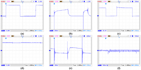
A practical prototype flyback converter with designed power circuit parameters according to Tables 1 and 2 has implemented for experimental verification of the proposed controller design approach. At first, the experimental results for the classic controller design approach and one pole-one zero case with circuit parameters depicted in Table 4 has implemented. Figure 7 shows the related results. The current of power switch has depicted in Figure 7(b) for 56 Ω load resistance. In the designed flyback converter, for sensing of switch current, a 1Ω resistor has located on switch source lead and its voltage has been filtered by a low pass RC filter with cutting frequency of 300 kHz. As can be seen from this figure, the converter operates in continuous operating mode. Figure 7(c)-7(e) depict the drain-source voltage of switch, converter output voltage and output voltage ripple respectively. It is obvious that the switch off-state voltage must be equal to source voltage and added referred output voltage to the primary side i.e., 48 volts. Also, Figure 7(e) shows that the designed snubber circuit can absorb the transformer stray inductance energy with a low voltage spike.
A good controller simultaneously, must have a good steady state and a good dynamic response. For SMPS converters the output voltage must be regulated at desired value with the least ripple as possible. Also the controller must have the ability to reject the external disturbances such as load and input voltage variations. The experimental results prepared here to discuss these two issues for the two designed controllers with classic and proposed approaches. As it can be seen from Figure 7(d)-7(e), the designed controller with classic approach could regulate the output voltage equal to desired value (12 Volts) and the output voltage has 0.2 volt peak to peak (1.5%) voltage ripple in steady-state. For studying the converter dynamic response, the load of that has been changed from half load (56 Ω) to full load (28 Ω) immediately by paralleling the second 56 Ω resistance. The result has been shown in Figure 7(f). As can be seen, the output voltage has a dynamic response with 0.5 volts (4%) undershoot and approximately 50 ms settling time similar to the simulation result.
Figure 6. Simulation results for error output signals with designed controllers: Limited band single pole controller with a) First order and b) Two order reference system and One pole-one zero controller with c) First order and d) Two order reference systems e) One pole-one zero controller with classic approach
Figure 7. Experimental results for designed one pole-one zero controller with classic approach: a) Gate pulse of power switch b) Current of power switch after low pass filter c) Drain-source voltage of power switch d) Output voltage e) Output voltage ripple f) Output voltage ripple for 50% step change of output load
Figure 8. Experimental results for designed one pole-one zero controller with proposed approach: a) Gate pulse of power switch b) Current of power switch after low pass filter c) Drain-source voltage of power switch d) Output voltage e) Output voltage ripple f) Output voltage ripple for 50% step change of output load
The experimental results of the proposed controller design approach for one pole-one zero case with circuit parameters depicted in Table 4 have shown in Figure 8. Beyond the similar results to the results that previously discussed, the dynamic response of the designed controller depicted in Figure 8(f) needs more attention. As can be seen, the output voltage has a better dynamic response with approximately 0.2 volt (1.5%) undershoot and 2 ms settling time compared with the controller designed with the classic approach. The experimental results summarized in Table 6.
Table 6. Summarized experimental results
|
Design Approach |
Steady State Output |
Steady State Ripple |
Load Dis. Undershoot |
Load Dis. Settling Time |
|
Classic |
12 V |
4% |
4% |
50 ms |
|
Proposed |
12 V |
4% |
1.5% |
2 ms |
In this paper, a novel controller design approach for DC-DC flyback converter based on the identification LS method has been proposed. The proposed method converts the controller design problem to the identification problem. As verified with simulation and experimental results, the proposed approach can design a controller with the desired structure and desired performance. These are two considerable advantages compared with common methods for classic linear controller design methods such as root-locus approach, frequency-domain method, Ziegler-Nichols method, adaptive self-tuning regulators and so on. Regard to these advantages, this approach is well suited for SMPS applications where benefit from analog controllers. The proposed idea is simple but it opens a new viewpoint in controller design using various and sophisticated identification methods and can be developed to use observer design methods, filter design methods and optimization methods. The main idea behind this approach is in all controller, observer, filter, identification and optimization design methods, mathematically an error must be minimized.
|
A |
DC gain |
|
D, d |
Switch duty cycle |
|
E, e |
Error signal |
|
Lm |
Magnetizing inductance (H) |
|
N |
Turn number of transformer windings |
|
n |
Primary to secondary turn ratio |
|
s |
Laplace variable |
|
Ts |
Sampling time (s) |
|
U, u |
Known matrix and vector |
|
Y |
Identification output vector |
|
Greek symbols |
|
|
θ |
Unknown parameters vector |
|
Subscripts
|
|
|
ESR |
Equivalent Series Resistance |
|
ex |
Extera |
|
c |
Controller |
|
cl |
Closed loop |
|
o |
Output |
|
p |
pole |
|
ref |
Reference |
|
s |
Source |
|
z |
Zero |
|
~ |
Indicate signal AC component |
$\begin{align} & G(s)=\frac{{{b}_{1}}s+{{b}_{0}}}{{{s}^{2}}+{{a}_{1}}s+{{a}_{0}}} \\ & {{b}_{1}}=\frac{1}{3}\times \frac{2{{L}_{m}}}{{{T}_{s}}{{V}_{s}}}\times \frac{-n{{L}_{m}}R{{I}_{Lm}}}{{{L}_{m}}RC}\times \frac{2.5}{12} \\ & {{b}_{2}}=\frac{1}{3}\times \frac{2{{L}_{m}}}{{{T}_{s}}{{V}_{s}}}\frac{Rn(1-D)(n{{V}_{o}}+{{V}_{s}})}{{{L}_{m}}RC}\times \frac{2.5}{12} \\ & {{a}_{1}}=\frac{2{{L}_{m}}}{{{T}_{s}}{{V}_{s}}}\times \frac{RC(n{{V}_{o}}+{{V}_{s}})}{{{L}_{m}}RC}+\frac{1}{RC} \\ & {{a}_{0}}=\frac{2{{L}_{m}}}{{{T}_{s}}{{V}_{s}}}\times \frac{n{{V}_{o}}+{{V}_{s}}+R{{n}^{2}}{{(1-D)}^{2}}{{I}_{Lm}}}{{{L}_{m}}RC}+\frac{R{{n}^{2}}{{(1-D)}^{2}}}{{{L}_{m}}RC} \\ \end{align}$ (A.1)
$\begin{align} & y=(T_{s}^{-3}+{{a}_{1}}T_{s}^{-2}+{{a}_{0}}T_{s}^{-1})\times ({{V}_{ref}}(k+3)-E(k+3)) \\ & -(3T_{s}^{-3}+2{{a}_{1}}T_{s}^{-2}+{{a}_{0}}T_{s}^{-1})\times ({{V}_{ref}}(k+2)-E(k+2)) \\ & +(3T_{s}^{-3}+{{a}_{1}}T_{s}^{-2})\times ({{V}_{ref}}(k+1)-E(k+1)) \\ & -T_{s}^{-3}\times ({{V}_{ref}}(k)-E(k)) \\ \end{align}$ (A.2)
$\begin{align} & {{u}_{1}}=-(T_{s}^{-2}+{{a}_{1}}T_{s}^{-1}+{{a}_{0}})\times ({{V}_{ref}}(k+2)-E(k+2)) \\ & +(2T_{s}^{-2}+{{a}_{1}}T_{s}^{-1})\times ({{V}_{ref}}(k+1)-E(k+1)) \\ & -T_{s}^{-2}\times ({{V}_{ref}}(k)-E(k)) \\ \end{align}$ (A.3)
${{u}_{2}}=({{b}_{1}}T_{s}^{-1}+{{b}_{0}})\times E(k+1)-{{b}_{1}}T_{s}^{-1}\times E(k)$ (A.4)
$\begin{align} & y=(T_{s}^{-4}+{{a}_{1}}T_{s}^{-3}+{{a}_{0}}T_{s}^{-2})\times ({{V}_{ref}}(k+4)-E(k+4)) \\ & -(4T_{s}^{-4}+3{{a}_{1}}T_{s}^{-3}+2{{a}_{0}}T_{s}^{-2})\times ({{V}_{ref}}(k+3)-E(k+3)) \\ & +(6T_{s}^{-4}+3{{a}_{1}}T_{s}^{-3}+{{a}_{0}}T_{s}^{-2})\times ({{V}_{ref}}(k+2)-E(k+2)) \\ & -(4T_{s}^{-4}+{{a}_{1}}T_{s}^{-3})\times ({{V}_{ref}}(k+1)-E(k+1)) \\ & +T_{s}^{-4}\times ({{V}_{ref}}(k)-E(k)) \\ \end{align}$ (A.5)
$\begin{align} & {{u}_{1}}=-(T_{s}^{-3}+{{a}_{1}}T_{s}^{-2}+{{a}_{0}}T_{s}^{-1})\times ({{V}_{ref}}(k+3)-E(k+3)) \\ & +(3T_{s}^{-3}+2{{a}_{1}}T_{s}^{-2}+{{a}_{0}}T_{s}^{-1})\times ({{V}_{ref}}(k+2)-E(k+2)) \\ & -(3T_{s}^{-3}+{{a}_{1}}T_{s}^{-2})\times ({{V}_{ref}}(k+1)-E(k+1)) \\ & +T_{s}^{-3}\times ({{V}_{ref}}(k)-E(k)) \\ \end{align}$ (A.6)
$\begin{align} & {{u}_{2}}=({{b}_{1}}T_{s}^{-2}+{{b}_{0}}T_{s}^{-1})\times E(k+2) \\ & -(2{{b}_{1}}T_{s}^{-2}+{{b}_{0}}T_{s}^{-1})\times E(k+1)+{{b}_{1}}T_{s}^{-2}\times E(k) \\ \end{align}$ (A.7)
${{u}_{3}}=({{b}_{1}}T_{s}^{-1}+{{b}_{0}})\times E(k+1)-{{b}_{1}}T_{s}^{-1}\times E(k)$ (A.8)
[1] Ned, M., Undeland, T.M., Robbins, W.P. (2003). Power Electronics: Converters, Applications and Design. John Wiley and Sons Inc.
[2] Terashi, H., Ninomiya, T. (2004). Analysis of leakage-inductance effect on characteristics of flyback converter without right half plane zero. The 4th International Power Electronics and Motion Control Conf. (IPEMC), Chicago, IL, USA, pp. 718-724. http://dx.doi.org/10.1109/INTLEC.2004.1401550
[3] Iqbal, H.K., Abbas, G. (2014). Design and analysis of SMC for second order DC-DC flyback converter. 17th IEEE International Multi Topic Conf, Karachi, pp. 533-538. http://dx.doi.org/10.1109/INMIC.2014.7097398
[4] Chen, S., Gu, Y., Lu, Z., Qian, Z., Yao, W. (2005). A transformer assisted ZVS scheme for flyback converter. 12th Applied Power Electronics Conf. and Exposition (APEC), Austin, TX, pp. 678-682. https://doi.org/10.1109/APEC.2005.1453040
[5] Chen, C.J., Cheng, C.H., Wu, P.S., Wang, S.S. (2019). Unified small-signal model and compensator design of flyback converter with peak-current control at variable frequency for USB power delivery, IEEE Trans. on Power Electron., 34(1): 783-793. http://dx.doi.org/10.1109/TPEL.2018.2812855
[6] Bogdan, A.I., Bizon, N. (2015). Voltage-mode control of the DC-DC power converter-a short review. 7th International Conference on Electronics, Computers and Artificial Intelligence (ECAI), Bucharest, pp. E-27-E-32. https://doi.org/10.1109/ECAI.2015.7301148
[7] Wan, K. (2009). Advanced current-mode control techniques for DC-DC power electronic converters. PhD thesis at Missouri University of Science and Technology.
[8] Li, Y., Zhu, Z. (2020). A constant current control scheme for primary-side controlled flyback controller operating in DCM and CCM. IEEE Trans. on Power Electron., 35(9): 9464-9472. http://dx.doi.org/10.1109/TPEL.2020.2972771
[9] Utkin, V. (2013). Sliding mode control of DC/DC converters. Journal of the Franklin Institute, 350(8): 2146-2165. http://dx.doi.org/10.1016/j.jfranklin.2013.02.026
[10] Said, O., Guo, L. (2013). PWM-based adaptive sliding-mode control for boost DC–DC converters. IEEE Transactions on Ind. Electron., 60(8): 3291-3294. http://dx.doi.org/10.1109/TIE.2012.2203769
[11] Salimi, M., Hajbani, V. (2015). Sliding-mode control of the DC-DC flyback converter in discontinuous conduction mode. 6th Power Electronics, Drives Systems & Technologies Conference (PEDSTC), Tehran, 2015, pp. 13-18. http://dx.doi.org/10.1109/PEDSTC.2015.7093242
[12] Houresh, A.B., Ershadi, M.H. (2019). Fuzzy control of the push-pull fly-back three-phase DC-DC converter. Modelling, Measurement and Control A, 92(1): 1-6. https://doi.org/10.18280/mmc_a.920101
[13] Brown, M. (2011). Power Supply Cookbook: 2nd Edition. Butterworth–Heinemann press.
[14] McLyman, C.W.T. (2011). Transformer and Inductor Design Handbook. CRC Press. http://dx.doi.org/10.1201/9780203913598
[15] Erickson, R.W., Maksimovic, D. (2001). Fundamentals of Power Electronics. 2nd Edition, Kluwer Academic Publishers. http://dx.doi.org/10.1007/b100747
[16] Pressman, A.I., Billings, K., Morey, T. (2009). Switching Power Supply Design: Third Edition, McGraw-Hill.
[17] Panday, S.K., Kumar, A., Patil, S.L. (2015). Large-signal model and nonlinear control of PWM converters in discontinuous conduction mode. 41st Annual Conference of the IEEE Industrial Electronics Society (IECON), Yokohama, pp. 003069-003074. http://dx.doi.org/10.1109/IECON.2015.7392571
[18] Texas Instruments Incorporation (2002). UC3845 datasheet. Document no.: SLUS223A.