Baban K. Suryatal* | Sunil S. Sarawade | Suhas P. Deshmukh
© 2020 IIETA. This article is published by IIETA and is licensed under the CC BY 4.0 license (http://creativecommons.org/licenses/by/4.0/).
OPEN ACCESS
The stereolithography (SL) process is one of the rapid prototyping technics and it is also known as additive layered manufacturing method. It is a chipless manufacturing method and the object is built layer by layer. A low cost stereolithography apparatus (SLA) is developed to produce highly precise, three-dimensional (3D) structures from broad selection of functional materials, especially photopolymer resin. The present SL systems available in the market are very expensive. The developed low cost SLA will be affordable to medium scale industries as well as customers. The developed SLA utilizes focused light beam of wavelength range of 300 nm – 700 nm from the DLP projector and passes through the objective lens over the surface of a photo-curable resin, which undergoes photo-polymerization and forms solid structures. The photopolymer used in this experimentation is polyethylene glycol di-acrylate and photo-initiator is Irgacure 784. The experiments are performed on objects with hexagonal cross-section and pyramid geometries and 0.1 mm curing depth along Z – axis. The trials are performed with different exposure and settling period. The 3D objects are successfully fabricated with high build speed and low cost. The pyramid object with maximum 120 numbers of layers with 12 mm dimension along Z-axis is built in 11.0 minutes. It is found that the optimum exposure time to cure a layer is two seconds. The maximum exposure area obtained in X-Y plane is 55 mm x 45 mm. The percentage dimensional error of the build objects is decreased as the curing time is reduced and the error is minimum for the two seconds curing period per layer. The obtained resolution of the build objects in X-Y plane is 23 microns and Z-stage resolution is 0.1 mm.
photo-polymer, stereolithography, rapid prototyping, ultra-violet light
There are a number of processes that can realize three-dimensional (3D) shapes such as those stored in the memory of a computer. An example is the use of holographic techniques [1], but these require many complex calculations to obtain the hologram and there is insufficient accuracy and clarity. A manual or a conventional mechanical process can also make a physical model, but such models require long fabricating times, high cost and excessive labour. To solve these kinds of problems, a new group of techniques called additive manufacturing (AM) technologies have been developed by a number of researchers group [2-5]. AM is a collection of processes in which physical objects are quickly created directly from computer generated models. The basic concept of rapid prototyping is where 3D structures are formed by laminating thin layers according to two-dimensional (2D) slice data, obtained from a 3D model created on a CAD/CAM system [2-5]. Stereolithography (SL) is one of the most popular AM process. It usually involves the curing or solidification of a liquid photosensitive polymer by focusing a light beam or laser beam of specific wavelength on the surface with liquid photopolymeric resin. The focused light beam supplies energy that induces a chemical reaction, bonding large number of small molecules and forming a highly cross-linked polymer [6]. Now a day, rapid prototypes of the different objects are required before their actual manufacturing because one can improve the design at the early stage of product development. The rapid prototyping or 3D printing field is very fast developing and this technology can applicable to all the fields i.e. engineering as well as non-engineering. The objective of this research work is to develop a low cost stereolithography apparatus (SLA) to produce highly precise, three-dimensional (3D) structures from broad selection of functional materials, especially photopolymer resin. The present SL systems available in the market are very expensive. The overall cost of the newly developed SLA is very low as compared to cost of SLA available in the market. The cost of photo-curable resin used is also low as compared to other available resins. Therefore, the developed low cost SLA will be affordable to medium scale industries and customers as the overall build cost of the objects is minimum.
A large number of researcher’s groups have developed the SL systems out of which some of them are briefed in the following literature review.
Fujimasa [7] has been described the concepts of microplanes, microrobots, microcars and microsubmarines and MEMS which are systems that combine computers with tiny mechanical devices such as sensors, valves, gears, mirrors, and actuators embedded in semiconductor chips. Ventura et al. [8] developed a direct photo shaping process for the fabrication of functional ceramic components layer by layer and each layer is photo image or a digital light processing (DLP) projection system. Bertsch et al. [9] developed a micro stereolithography apparatus employing a pattern generator in which a UV laser and dynamic LCD pattern generator were used to generate the cross section of a 3D structure. While the substrate did not move in the x–y direction in the liquid photopolymer, an LCD pattern generation system was necessary and the resulting diffraction had to be considered. Maruo et al. [10] developed two-photon polymerization (TPP) which utilizes focused lasers to precisely polymerize small volumes resin and the volume is only polymerized if it is excited by two different photons within a very short time period. TPP is much slower than SL, but has successfully created components with 100 nm features. TPP is limited to polymers because it requires a clear resin to function; suspended particles would scatter the laser beams. Young et al. [11] have described a novel device for producing 3D objects that has been developed using an LCD as a programmable, dynamic mask and visible light to initiate photopolymerization. Ikuta et al. [12] introduced micro stereolithography technology and proposed a means of applying micro stereolithography in mass-production using an optical fiber array so that multiple microstructures could be fabricated in a single process. Monneret et al. [13] presented a new process of microstereolithography to manufacture freeform solid 3D micro-components with outer dimensions in the millimeter size range. Sun et al. [14] performed Monte Carlo simulations and experimental studies to understand the detailed microscale optical scattering, chemical reaction (polymerization), and their influence on critical fabrication parameters. It was found that due to the scattering, the fabricated line is wider in width and smaller in depth compared with polymeric fabrication at the same condition. The doping technique substantially reduced the light scattering, which in turn enhanced the fabrication precision and control. The experimental values of curing depth and radius agreed reasonably well with the theoretical modeling. Bertsch et al. [15] described new polymer/composite photosensitive resins that can be used in the microstereolithography process for manufacturing complex 3D components. Huang et al. [16] analyzed the shrinkage deformation of the mask type stereolithography process. Lee et al. [17] developed a micro stereolithography apparatus using a UV laser and a complex optical system. Jiang et al. [18] developed a Masked Photopolymerization Rapid Prototyping (MPRP) system using LCD panel as dynamic mask with an upper exposure skill. Dongkeon et al. [19] developed a liquid crystal display (LCD) based micro stereolithography process in order to fabricate microparts with superior mechanical properties (for e.g., micro gears) and investigates the fabrication process of micro bevel gears using photosensitive resins reinforced with ceramic nanoparticles. Deshmukh et al. [20] proposes and develops an offaxis lens scanning technique for MSL and carries out optical analysis to compare its performance with the existing techniques mentioned above. The comparison clearly demonstrates improved performance with the proposed offaxis lens scanning technique. Limaye [21] presented a more sophisticated process planning method to build a part with constraints on dimensions, surface finish and build time and formulated an adaptive slicing algorithm that slices a CAD model so as to obtain the required trade-off between build time and surface finish of up facing surfaces of the part. Hadipoespito et al. [22] developed DMD based UV micro – stereolithography system for fabricating 2D and 3D micro – parts. With the help of characterization experiments it was observed that the developed the DMD based imaging system irradiates an entire photopolymer layer at once, providing reasonable curing speed and good resolution at a low cost. Micro parts were also fabricated in nanocomposites, which were obtained by ultrasonic mixing of the transparent photopolymer and nano-sized ceramic particles. The micro models fabricated by this process could be used for micro scale investment casting, tooling, devices, and medical applications. In this method process optimization is needed to improve the quality of fabricated micro – parts. Singhal et al. [23] has presented a statistical surface roughness model for SLS prototypes as a key to slice the tessellated CAD model adaptively. The adaptive slicing system is implemented as Graphic User Interface in MATLAB-7.
Choi et al. [24] developed a more economical and simpler micro-stereolithography technology using a UV lamp as a light source and optical fiber as the light delivery system and photopolymer solidification experiments were conducted to examine the characteristics of the developed micro-stereolithography apparatus. Zhao et al. [25] developed a thick film mask projection stereolithography to fabricate films on fixed flat substrate and develop a column cure model in which a CAD model of part is discretized into vertical columns instead of being sliced into horizontal layers, and all columns get cured simultaneously till the desired heights. Vatani et al. [26] optimized the exiting slicing algorithms for reducing the size of the files and memory usage of computers to process them. In spite of type and extent of the errors in STL files, the tail-to-head searching method and analysis of the nearest distance between tails and heads techniques were used. As a result STL models sliced rapidly, and fully closed contours produced effectively and errorless. Deshmukh et al. [27] carried out analysis and experimental verification of optomechanical scanning systems for microstereolithography. Choi et al. [28] developed MSL system for tissue engineering using a Digital Micromirror Device (DMD) for dynamic pattern generation and an ultraviolet (UV) lamp filtered at 365 nm for crosslinking the photoreactive polymer solution. Gandhi et al. [29] proposes and analyses a 2D optomechanical-focused laser spot scanning system for microstereolithography which allows uniform intensity focused spot scanning with high speed and high resolution over a large range of scan. Higher speed and high resolution at the same time are achieved by use of two serial double parallelogram flexural mechanisms with mechatronics developed around them. Itoga et al. [30] developed maskless photolithography device by modifying Liquid Crystal Display (LCD) projector optics from magnified to reduced projection. The developed device produces a practical centimeter scale micro-pattern by dividing a large mask pattern and divisionally exposing it synchronized with an auto – XY stage, applying it to cell micro-pattern and microfluidic device production. But they arise problems in jagged pattern boundaries due to the liquid crystal panel structure and collapse pattern of the boundary divided on divisional exposure using the auto – XY stage. Zhou et al. [31] presented a novel AM process based on the mask video projection. For each layer, a set of mask images instead of a single image are planned based on the principle of optimized pixel blending. Experimental results show that the mask video projection process can significantly improve the accuracy and resolution of built components. The disadvantage of this method is that it will require an additional linear stage with good accuracy and moving speed. In addition, the platform movement during the building process requires the designed hardware to ensure the repeatability between different layers which increases the overall cost of the system. Zabti [32] carried out Pareto based Multi-objective function based optimization of STL process which has three objective functions. The goal is to find the optimum exposure time value by minimizing the cure depth, surface roughness and maximizing the mechanical strength. Lehtinen [33] developed a DMD based projection stereolithography and a computer code is written to control the entire manufacturing process. Gandhi et al. [34] analyze various optical scanning schemes used for MSL systems along with the proposed scheme via optical simulations and experiments. The mechanical design of the scanning mechanism is carried out to meet requirements of high speed and resolution. The system integration and investigation in process parameters is carried out and fabrication of large micro-component with high resolution is demonstrated. Campaigne III [35] developed projection stereolithography and material characterization of nanocomposites photopolymers was carried out. Valentincic et al. [36] conclude that DLP based stereolithography is used to reduce the build time and to increase the manufacturing accuracy. Compared to fused deposition modeling (FDM) machines, machines for DLP stereolithography are expensive and thus not available to a broad range of users as it is the case with FDM 3D printers. Luo et al. [37] developed desktop manufacturing system which can produce RP parts with good machining efficiency, but the surface roughness should be further improved. Ibrahim et al. [38] investigate the influence of process parameters which are layer thickness and exposure time on physical and mechanical properties of DLP structure.
Thus, by going through the aforementioned literature on SL systems, it is observed that most of researchers develop microstereolithography systems. The developed SL systems are either LCD based or DMD based. The disadvantages of LCD based SL systems are low pixel filling ratio, print – through errors occurs due to light that penetrates into already cured layers, unnecessary wavelengths cause inaccurate dimensions in the cured part. The advantages of DMD based SL systems are availability of UV compatibility, high modulation efficiency, high light transmission, high optical fill factor, low pitch size and pixel size. Both the developed SL systems i.e. LCD as well as DMD based mentioned in above literature survey are very expensive, which are not affordable to common or medium sized industries or vendors who can build their prototypes with a cheaper cost. Therefore, development of a low cost SLA with better build speed is a goal of this research work.
The sub-section 2.1 of section 2 describes the developed low cost SLA in detail with specifications of the sub-systems, different softwares, photo-polymer and photo-initiator used in the apparatus. In sub-section 2.2 the absorbance spectrum of photo-curable resin and light beam spectrum of DLP projector are plotted. In sub-section 2.3 the slicing procedure of 3D CAD model into 2D slices is explained with the help of developed MATLAB code. The experimental results and discussions are given in section 3. Finally, the conclusions are drawn from experimental work in section 4.
2.1 Stereolithography apparatus (SLA)
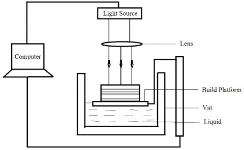
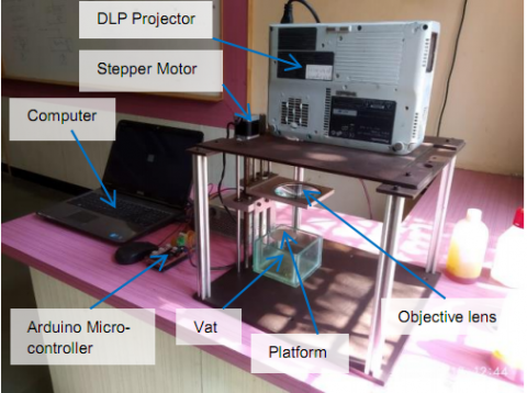
The stereolithography apparatus (SLA) is developed to produce highly precise, three-dimensional (3D) structures from broad selection of functional materials, especially photopolymer resin. The lay-out of the experimental set-up is shown in Figure 1 and the CAD model is shown in Figure 2. The developed stereolithography apparatus (SLA) utilizes focused light beam from DLP projector and then through the objective lens over the surface of a photo-curable resin, which undergoes photo-polymerization and forms solid structures. The lamp of the modified DLP projector works as light source and DMD chip in the DLP projector works as a dynamic pattern generator for this SLA. The colour wheel of the DLP projector is filtering most of the UV light out. But UV light is required for solidification of the photopolymer. Therefore, we had done changes in the colour wheel. The color wheel is a glass disc with several colored segments that spins while the projector is running to colorize the image. The projector actually requires it to run; when the color wheel is simply removed, the projector would not turn on the lamp. Therefore, only glass portion of the color wheel is removed so that maximum UV light should come out from the projector which is the requirement for solidification of liquid resin. After removing glass portion from the color wheel, the projector becomes black and white. Infocus make DLP projector with display resolution 1024×768 is used. The photograph of actual experimental set-up is shown in Figure 3.
Figure 1. Lay-out of the experimental set –up
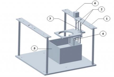
1-Frame, 2-Ball Screw, 3-Guide rod, 4-Z stage, 5-Resin Tank, 6-Stepper motor
Figure 2. CAD model of experimental set-up without DLP projector
Figure 3. Experimental set-up
The photopolymer used in this experimentation is polyethylene glycol di-acrylate with 2% Irgacure 784 as photo-initiator. The absorbance spectrum of the photopolymer is plotted and the maximum absorbance observed is in the range of 315 nm to 480 nm. The peak absorbance of polyethylene glycol di-acrylate matches with the peak intensity of light beam of DLP projector which is in the range of 400 nm – 570 nm. Therefore, polyethylene glycol di-acrylate is selected as photo-curable resin and cost of the same resin is also low as compared to other resins. From this data it is concluded that maximum UV light is required for solidification of the photopolymer. The NEMA 17 bipolar stepper motor with 0.9˚ step angle, 5% step accuracy, 5 mm shaft diameter is used to rotate the ball screw. The ball screw with nominal diameter 12 mm, pitch 2.0 mm, core diameter 10.084 mm and lead angle 3.04˚ is used for up and down motion of the Z-stage. The maximum speed of the stepper motor is 2344 rpm and holding torque is 4.8 kg-cm. The Creo 3.0 software is used for modeling of 3D CAD model. The 3D CAD model and STL file format in Creo 3.0 software is more compatible with developed MATLAB code for slicing of 3D CAD model as compared to other modeling softwares. Therefore, Creo 3.0 software is selected for 3D CAD modeling. A special MATLAB code is developed for slicing of the 3D CAD model and this sliced 3D CAD model is imported into the Creation Workshop software version 1.0.0.75 which is used to control the focusing time period of sliced images through DLP projector and focusing lens. The make of focusing lens is Optics and Allied Engineering Private Limited, Bangalore with 100 mm diameter and 100 mm focal length. The Creation Workshop software also controls the motion of the Z-stage through Arduino MEGA 2560 micro- controller and NEMA 17 bipolar stepper motor. It also controls input parameters, such as layer thickness, motor movement speed, exposure time and settling period. These parameters make the equipment versatile and suitable for a wide range of different tasks. Finally, the different shape objects are built by curing the aforementioned photo-curable resin. The photographs of the build components are taken by the Amp Cam digital microscope with optimum resolution 640×480 and 5X digital zoom. The FARO Edge 3D scanner with the specifications ±25µm accuracy, 25µm repeatability, 115 mm depth of field, 80 mm effective scan width for near field, 2,000 scanning points per line, 40µm minimum point spacing, 280 frames/second scan rate and Class 2M laser is used to measure the dimensions of the build objects. Thus, a low cost, high build speed SLA is developed to fabricate 3D components.
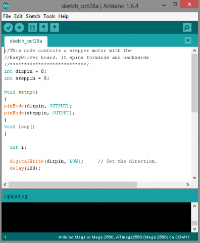
In the Z- Stage, we have to control the linear movement of the platform with the help of stepper motor and ball screw. The stepper motors rotational motion is transformed in to linear motion with help of ball screw coupled with motor shaft. Arduino microcontroller is used for precise and accurate control the movement of the motion stage. The rotational movement of the stepper motor is controlled with the help of special Arduino program. The program mainly consists of various commands and statements to control the various parameters such as speed, time delay etc. Figure 4 shows the window of Arduino software in which the uploaded program is shown. The Arduino Micro-controller with stepper motor is interfaced with Creation Workshop Software to obtain desired motion of Z-stage.
Figure 4. The program uploaded to the Arduino software
2.2 Spectrum study of photopolymer and DLP projector
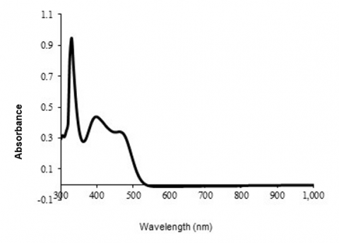
The 3D object is built by focusing the light beam of DLP projector through objective lens on the z-stage platform. On the Z-stage platform a layer of liquid photopolymer of thickness equal to the slice thickness of CAD model is made available by lowering the platform with help of ball screw and stepper motor. Therefore, it is necessary to plot the absorbance spectrum of photopolymer from which we can conclude that what is value of wave length for peak absorbance. The Figure 5 shows the absorbance spectrum plot of photopolymer and it is observed that the peak absorbance is at wavelength 335 nm, 410 nm and 480 nm. Therefore, the focused light beam must have the peak wavelength in the range of 300 – 500 nm which is a UV light region.
Figure 5. Absorbance spectrum of photopolymer
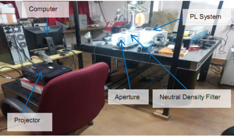
Figure 6. DLP projector light beam spectrum plotting set-up
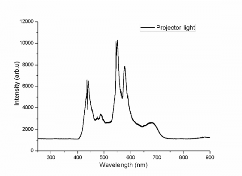
Figure 7. Light beam spectrum of DLP projector
The study of DLP light beam spectrum is done by using Horriba (model iHR320) light spectrometer. The Figure 6 shows the set-up for plotting the spectrum of DLP projector light beam. The light beam from the DLP projector is passes through the aperture then it passes through the neutral density filter. The neutral density filter removes the unwanted light rays. The spectrum is plotted for the light wavelength range of 250 – 900 nm. Finally, light beam passed into the photoluminescence (PL) system. The PL system consists of optical grating, mirror 1 and mirror 2 with CCD (closed circuit device) camera. The measured spectrum data by PL system is collected by the computer. The Figure 7 shows the light beam spectrum obtained by above mentioned spectrometer. From light beam spectrum it is observed that the peak values are in the wavelength range of 400 nm – 570 nm. Therefore, the light beam of DLP projector is useful to cure the selected photopolymer as peak wavelength range matches with each other.
2.3 Slicing of 3D CAD model
Basically, the stereolithography equipment consists of a DLP projector, focusing lens, resin vat, a linear translation stage with a platform and a computer. Before the manufacturing can begin, some preparations must be done. First, the CAD model is sliced into horizontal cross-section images. These black and white images will be projected one by one onto the platform with resin layer. As there are different methods available to slice a CAD model without tessellation but slicing a triangulated mesh model is still the commonly used method in 3D printing caused by its format (i.e. STL) is widely adopted in software and machine. These different methods of slicing a 3D CAD models are Contour, Voxelization and Ray tracing [39]. The contour method is the traditional slicing process that generates the cross-sectional information by intersecting the input model with a set of horizontal planes. As the input model is tessellated into faces (e.g. triangles defined in the STL), the slicing operation is actually a number of face-plane intersections, each of which is a segment. In a layer, the intersection between the model and a slicing plane is one or more polygons (contours), which are constituted by the segments. The voxelization method creates a 3D array of voxels that can cover the whole volume of the input model, and then decides whether each voxel is inside or outside the model. The in/out determination is challenging, because the mesh is just a set of faces in the 3D space without the information of inside or outside. In ray-tracing method, 2D image is used and in/out for every pixel in a slice is determined similar to point-in-polygon testing. In this method testing can be done by casting a ray from each pixel to intersect with the model, and finding out if the ray reaches the interior or exterior of the model at a particular height. Out of the above three slicing technologies, the ray-tracing method is the fastest in most cases and it needs a moderate amount of memory for computation. It maintains a good balance between computation time and memory space. It would be optimal if the intersection problem can be handled without creating other problems. Therefore, due to these advantages, the ray-tracing method is used for development of a special MATLAB code for slicing of 3D CAD model in this research work.
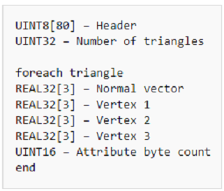
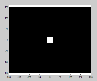
The STL file shown in Figure 8 was originally conceived by 3D Systems [40] and it opened the door for rapid prototyping and manufacturing market by allowing CAD data to be used in STL systems. The file consists of an unordered list of triangular facets that represent the outside skin of a part. The triangular facets are described by a unit normal vector and a set of X, Y, Z coordinates for each of the three vertices. The unit vectors indicate the outside of the part. Since the STL model consists of triangular facets, it is an approximate model of the accurate CAD data. Regardless of being an imprecise model, STL has become the standard used by most CAD and RP systems. STL is a simple solution for representing 3D CAD data and it provides small and accurate files for data transfer for specific shapes [41, 42]. There are two formats for STL file: ASCI and Binary which are shown in Figure 9 and Figure 10 respectively. Binary files are smaller and more compact. Hence, they are more common. After generating the STL file of the 3D CAD model then it is necessary to slice the model into a number of horizontal cross-section images. The 3D CAD model of the object which is to be built by using stereolithography process is developed with the help of CREO 3.0 software. Then it is saved in STL file format using the same software. The Figure 11 shows the 3D CAD model in STL file format.
Figure 8. Standard Tessellation Language (STL) file and CAD model [42]
Figure 9. ASCII STL file format [42]
Figure 10. Binary STL file format [42]
Figure 11. 3D CAD model in STL file format
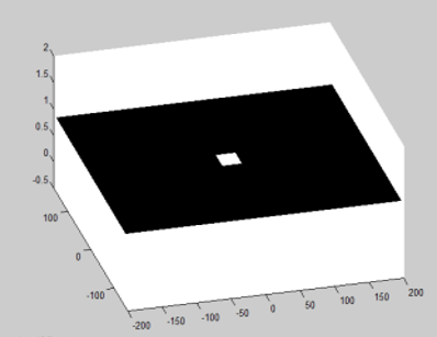
Thus, a special MATLAB code is developed by using ray tracing method and by using this code, the 3D CAD model is sliced into a number of layers as shown in Figure 12. The Figure 13 (a) and (b) shows a single sliced layer in MATLAB software window. Then these sliced layers are imported in Creation Workshop software and focused one by one at required time interval with the help of DLP projector through objective lens on the Z- stage platform and finally the 3D object is built.
Figure 12. Sliced 3D CAD model
(a)
(b)
Figure 13. 2D Slices in MATLAB window
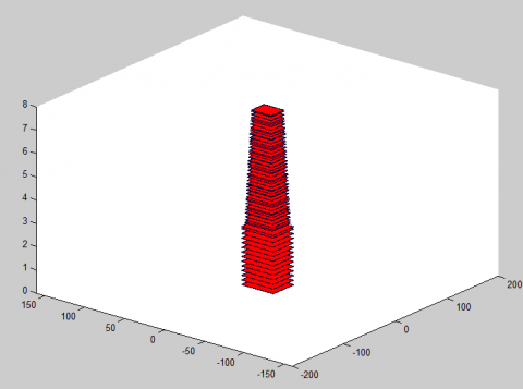
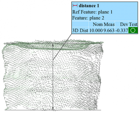
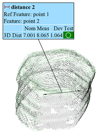
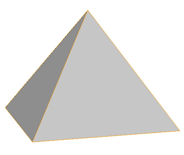
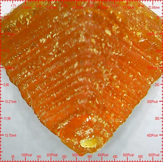
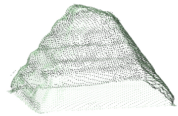
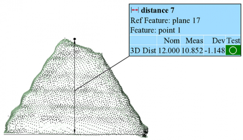
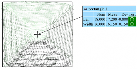
The experiments are performed with hexagonal cross-section and pyramid objects with 0.1 mm curing depth along Z – axis. The trials are performed with different exposure time and settling period. The exposure time is varied from 10 seconds to 1 second and it is observed that the objects are best cured for 2 seconds curing period. The experimental test data for hexagonal cross-section and pyramid objects are given in Table 1 and Table 2 respectively. The CAD model of the hexagonal prism is shown in Figure 14 and scanned image of build hexagonal prism by FARO Edge 3D scanner is shown in Figure 15. The built hexagonal prism is shown in Figure 16 (a) and (b). The Figure 17 shows the measurements of dimensions of hexagonal prism by FARO Edge 3D scanner. The Figure 18 shows the CAD model of pyramid and Figure 19 shows the built pyramid. The scanned image of built pyramid by FARO Edge 3D scanner is shown in Figure 20 and the measurement of dimensions of pyramid by FARO Edge 3D scanner are shown in Figures 21-23. The pyramid object with 120 numbers of layers with 12 mm dimension along Z-axis is built. The maximum area 18 mm x 16 mm of pyramid object along X-Y plane is cured. For commercial SLA machines resolution in Z-axis is in between 0.01 to 0.25 mm. The resolution along Z-axis of 0.25mm creates a fairly coarse surface for medium sized parts, but for larger models, the layer steps are not too noticeable due to the relative size of larger parts. A resolution of 0.1mm provides a more favorable surface finish for medium and small parts. Therefore, experiments are performed with 0.1 mm curing depth along Z-axis. The maximum exposure area obtained is 55mm x 45mm. It is observed that as the curing time decreases the percentage error between the 3D CAD model dimensions and built dimensions are also decreases. The maximum and minimum percentage errors for hexagonal cross-section object are 9.43 and 2.0 respectively. The maximum and minimum percentage errors for pyramid object are 4.44 and 0.93 respectively. The minimum percentage error is observed for 2 seconds curing period. The dimensions of the built components are measured by FARO Edge 3D scanner with ±25µm accuracy. Creation Workshop software Version 1.0.0.75 is used: (i) to control the Z-stage motion, (ii) to control the focusing time of sliced images and settling time. The resolution of the built components depends upon Software Imposed Parameters (SIP) and SL Process Parameters (PP). The Software Imposed Parameters (SIP) are line width compensation, .stl file resolution, layer thickness, z compensation, and stereolithography grid. The SL Process Parameters (PP) consists of light beam size and intensity, light beam focus depth, and layer thickness [43].
Figure 14. CAD model of hexagonal prism
Figure 15. Scanned image of build hexagonal prism
(a)
(b)
Figure 16. Built hexagonal prism
Table 1. Hexagonal prism experimentation data
|
Object Cross-section |
Measuring Scale |
Dimensions (mm) |
Layer thickness (mm) |
No. of layers |
Exposure time (sec.) |
Settling Period (sec.) |
Build time (sec.) |
||
|
x |
y |
z |
|||||||
|
Hexagon (7 mm side) |
CAD Model |
14 |
14 |
10 |
0.1 |
100 |
2 |
3.5 |
546.5 |
|
Built object |
15.32 |
14.28 |
9.66 |
||||||
|
% Error |
9.43 |
2.0 |
3.4 |
||||||
Table 2. Pyramid experimentation data
|
Object Cross-section |
Measuring Scale |
Dimensions (mm) |
Layer thickness (mm) |
No. of layers |
Exposure time (sec.) |
Settling Period (sec.) |
Build time (sec.) |
||
|
x |
y |
z |
|||||||
|
Pyramid |
CAD Model |
18 |
16 |
12 |
0.1 |
120 |
2 |
3.5 |
656.5 |
|
Built object |
17.20 |
16.15 |
10.85 |
||||||
|
% Error |
4.44 |
0.93 |
2.33 |
||||||
(a)
(b)
Figure 17. Measurement of height and side of hexagonal prism
Figure 18. CAD Model of pyramid
Figure 19. Built pyramid
Figure 20. Scanned Image of build pyramid
Figure 21. Height measurement of build pyramid
Figure 22. Base measurement of pyramid
Figure 23. Faro edge 3D scanner
A low cost stereolithography apparatus (SLA) has been developed with DLP projector as a UV light source. The overall cost of the developed SLA is very low as compared to the present commercial SLA available. Therefore, the build cost of the fabricated objects is reduced due to developed low cost SLA. The optimum curing period per layer is two seconds per layer as the percentage error is minimum for two seconds curing period. Therefore, build speed obtained is two seconds per layer which is remarkable compared with present SLA. The dimensional accuracy of fabricated objects is also satisfactory as the maximum and minimum percentage error is 9.43 and 0.93 respectively which is acceptable comparing with the results available in the literature [33, 36]. The dimensional percentage error is decreased as the curing period or image focusing period is reduced. The pyramid object with maximum 120 numbers of layers with 12 mm dimension along Z-axis is built in 11 minutes. The maximum exposure area obtained which can be cured in X-Y plane is 55 mm x 45 mm. The resolution of the build objects in X-Y plane is 23 microns which is resolution of sliced image focused from DLP projector and Z-stage resolution is 0.1 mm. The advantages of the developed SLA are low build cost, high fabrication speed, excellent resolution in X-Y plane, low resin cost etc. The limitations are low dimensional accuracy, poor resolution of the fabricated objects along Z-stage. The future scope of the work is to introduce the dimensional error correction model in the experimentation to minimize the percentage errors of the build objects. Another future scope is to perform the experiments with values lower than 0.1 mm curing depth so that resolution of build objects along Z- stage will be improved.
The authors are thankful to the Board of Colleges and University Development (BCUD) of Savitribai Phule Pune University, Pune for funding this research project under the grant number OSD/BCUD/360/122. The authors are also thankful to Dr. S. H. Gawande Professor, M.E.S. College of Engineering, Pune for technical support and Management, Principal Dr. R. V. Patil of Pune District Education Association’s College of Engineering, Manjari (Bk.), Pune for permitting to carry out this research work.
|
3D |
three dimensional |
|
AM |
additive manufacturing |
|
CAD CAM |
computer aided design computer aided manufacturing |
|
DLP DMD LCD MEMS MSL PL RP SL SLA STL UV |
digital light processing digital micro-mirror device liquid crystal display micro-electro-mechanical systems microstereolithography photoluminescence rapid prototyping stereolithography stereolithography apparatus standard tessellation language ultra-violet |
[1] Wilson, J., Hawkes, J.F.B. (1987). Lasers, Principles and Applications. Prentice Hall, New York.
[2] Gibson, I., Rosen, D.W., Stucker, B. (2009). Additive manufacturing technologies: Rapid Prototyping to Direct Digital Manufacturing, Springer, New York.
[3] Chua, C.K., Leong, K.F., Lim, C.S. (2003). Rapid Prototyping – Principles and Applications. World Scientific Publishing, Singapore.
[4] Gibson, I. (2006). Rapid prototyping from product development to medicine. Virtual and Physical Prototyping, 1(1): 31-42. http://dx.doi.org/10.1080/17452750500271298
[5] Bidanda, B., Bartolo, P.J. (2008). Virtual prototyping and Bio-manufacturing in medical applications. Springer, New York. http://dx.doi.org/10.1007/978-0-387-68831-2
[6] Fouassier, J. (1995). Photoinitiation, Photopolymerization, and Photocuring: Fundamentals and Applications. Hanser.
[7] Fujimasa, I. (1996). Micromachines: A New Era in Mechanical Engineering. Oxford University Press.
[8] Ventura, S.C., Narang, S.C., Sharma, S., Stotts, J., Liu, C., Liu, S., Ho, L.H., Annavajjula, D., Lombardi, S.J., Hardy, A., Mangaudis, M., Chen, E., Groseclose, L. (1996). A new SFF process for functional ceramic components. Proceedings of the Solid Freeform Fabrication, pp. 327-334.
[9] Bertsch, A., Zissi, S., Jezequel, J., Corbel, S., André, J. (1997). Microstereolithography using liquid crystal display as dynamic mask-generator. Microsystems Technologies, 3(2): 42-47. https://doi.org/10.1007/s005420050053
[10] Maruo, S., Kawata, S. (1998). Two-photon-absorbed near-infrared photopolymerization for three-dimensional microfabrication. Journal of Microelectromechanical Systems, 7(4): 411–415. http://dx.doi.org/10.1109/84.735349
[11] Young, J.S., Fox, S.R., Anseth, K.S. (1999). A novel device for producing three dimensional objects. Journal of Manufacturing Science & Engineering, 121(3): 474-477. http://dx.doi.org/10.1115/1.2832705
[12] Ikuta, K., Hirowatari, K. (1993). Real three-dimensional microfabrication using stereolithography and metal mold. Proceedings of IEEE International Workshop on Micro Electro Mechanical Systems (MEMS’93), pp. 42–47.
[13] Monneret, S., Le, G., Bade, H., Devaux, V., Mosset, F., Lantz, A. (2002). Dynamic UV microstereolithography. Applied Physics, 6(3): 213-218. http://dx.doi.org/10.1051/epjap:2002094
[14] Sun, C., Zhang, X. (2002). Experimental and numerical investigations on Microstereolithography of ceramics. Journal of Applied Physics, 92(8): 4796. http://dx.doi.org/10.1063/1.1503410
[15] Bertsch, A., Jiguet, S., Renaud, P. (2003). Microfabrication of ceramic components by microstereolithography. Journal of Micromechanics and Microengineering, 14(2): 197-203. http://dx.doi.org/10.1088/0960-1317/14/2/005
[16] Huang, Y.M., Jiang, C.P. (2003). Numerical analysis of a mask type stereolithography process using a dynamic finite element method. The International Journal of Advanced Manufacturing Technology, 21(9): 649-655. http://dx.doi.org/10.1007/s00170-002-1388-x
[17] Lee, I.H., Cho, D.W., Lee, E.S. (2004). Development of microstereolithography systems for the fabrication of three-dimensional micro-structure. Journal of Korean Society Precision Engineering, 21(2): 29-36. https://doi.org/10.1007/s00170-008-1461-1
[18] Jiang, C.P., Jeng, J.Y., Huang, Y.M., Tsai, M.J. (2005). Development of masked photo-polymerization rapid prototyping system using liquid crystal display panel. Journal of the Chinese Institute of Industrial Engineers, 22(1): 76-81. http://dx.doi.org/10.1080/10170660509509279
[19] Lee, D., Miyoshi, T., Takaya, Y., Ha, T. (2006). 3D microfabrication of photosensitive resin reinforced with ceramic nanoparticles using LCD micro stereolithography. Journal of Laser Micro/Nano Engineering, 1(2): 142-148.
[20] Deshmukh, S.P., Dubey, S., Gandhi, P.S. (2006). Optical analysis of scanning micro stereolithography systems. Micromachining and Microfabrication Process Technology XI, Proceedings, 61090C. http://dx.doi.org/10.1117/12.645856
[21] Limaye, A.S. (2007). Multi-objective process planning method for mask projection stereolithography. PhD dissertation, Georgia Institute of Technology.
[22] Hadipoespito, G.W., Yang, Y., Choi, H., Ning, G., Li, X. (2003). Digital micromirror device based microstereolithography for micro structures of transparent photopolymer and nanocomposites. Department of Mechanical Engineering University of Wisconsin-Madison, Madison, WI 53706.
[23] Singhal, S.K., Jain, P.K., Pandey, P.M. (2008). Adaptive slicing for SLS prototyping. Computer-Aided Design and Applications, 5(1-4): 412-423. http://dx.doi.org/10.3722/cadaps.2008.412-423
[24] Choi, J., Kang, H.W., Lee, I.H., Ko, T.J. (2009). Development of micro-stereolithography technology using a UV lamp and optical fiber. International Journal of Advance Manufacturing Technology, 41: 281-286. https://doi.org/10.1007/s00170-008-1461-1
[25] Zhao, X. (2009). Process planning for thick-film mask projection micro-stereolithography. PhD thesis, Georgia Institute of Technology.
[26] Vatani, M., Rahimi, A.R., Brazandeh, F., Sanatinezhad, A. (2009). An enhanced slicing algorithm using nearest distance analysis for layer manufacturing. World Academy of Science, Engineering and Technology, 3(1): 74-79. https://doi.org/10.5281/zenodo.1082905
[27] Deshmukh, S.P., Gandhi, P.S. (2009). Optomechanical scanning systems for microstereolithography (MSL): Analysis and experimental verification. Journal of Materials Processing Technology, 209(3): 1275-1285. http://dx.doi.org/10.1016/j.jmatprotec.2008.03.056
[28] Choi, J.W., Wickera, R., Leeb, S.H., Choi, K.H., Had, C.S., Chung, I. (2009). Fabrication of 3D biocompatible/biodegradable micro-scaffolds using dynamic mask projection microstereolithography. Journal of Materials Processing Technology, 209(15-16): 5494–5503. http://dx.doi.org/10.1016/j.jmatprotec.2009.05.004
[29] Gandhi, P.S., Deshmukh, S.P. (2009). A 2D optomechanical focused laser spot scanner: Analysis and experimental results for microstereolithography. Journal of Micromechanics and Microengineering, 20(1): 15-35. http://dx.doi.org/10.1088/09601317/20/1/015035
[30] Itoga, K., Kobayashi, J., Yamato, M., Okano, T. (2010). Development of microfabrication technology with maskless photolithography device using LCD projector. Journal of Robotics and Mechatronics, 22(5): 608-612. http://dx.doi.org/10.20965/jrm.2010.p0608
[31] Zhou, C., Chen, Y. (2011). Additive manufacturing based on optimized mask video projection for improved accuracy and resolution. Proceedings of NAMRI/SME, 14(2): 107-118. http://dx.doi.org/10.1016/j.jmapro.2011.10.002
[32] Zabti, M.M. (2012). Effects of Light Absorber on micro stereolithography parts. PhD thesis, School of Mechanical Engineering, The University of Birmingham, Edgbaston, Birmingham.
[33] Lehtinen, P. (2013). Projection microstereolithography equipment. MS thesis, School of Science, Aalto University.
[34] Gandhi, P.S., Deshmukh, S.P., Ramtekkar, R., Bhole, K., Baraki, A. (2013). “On-axis” linear focused spot scanning microstereolithography system: optomechtronic design, analysis and development. Journal of Advanced Manufacturing Systems, 12(01): 43-68. http://dx.doi.org/10.1142/S0219686713500030
[35] Campaigne III, E.A. (2014). Fabrication and Characterization of Carbon Nanocomposite Photopolymers via Projection Stereolithography. MS Thesis, Virginia Polytechnic Institute and State University, USA.
[36] Valentincic, J., Perosa, M., Jerman, M., Sabotin, I., Lebar, A. (2017). Low cost printer for DLP stereolithography. Journal of Mechanical Engineering, 63(10): 559-566. http://dx.doi.org/10.5545/sv-jme.2017.4591
[37] Luo, R.C., Tzou, J.H. (2010). Development of a LCD Photomask Based Desktop Manufacturing System. Motion Control, Federico Casolo (Ed.), ISBN: 978-953-7619-55-8, http://dx.doi.org/10.1109/TIE.2008.922603
[38] Ibrahim, A., Saude, N., Ibrahim, M. (2017). Optimization of process parameter for digital light processing (DLP) 3D printing. Proceedings of Academics World 62nd International Conference, Seoul, South Korea, 18th -19th April 2017, pp. 11-14.
[39] Kwok, T.H. (2017). Comparing slicing technologies for digital light processing printing. ASME, Department of Mechanical, Industrial and Aerospace Engineering Concordia University Montreal, Canada, 19(4): 044502. http://dx.doi.org/10.1115/1.4043672
[40] 3D Systems (1988). Stereolithography Interface Specification, Inc.
[41] Chua, C., Leong, K., Lim, C. (2010). Rapid Prototyping: Principles and Applications. Third edition, World Scientific.
[42] Jacobs, P., Reid, D. (1992). Rapid Prototyping and Manufacturing: Fundamentals of Stereolithography. Society of Manufacturing Engineers.
[43] Sager, B., Rosen, D. (2002). Stereolithography Process Resolution, The George W. Woodruff School of Mechanical Engineering Georgia Institute of Technology Atlanta, USA.