V. Madhurima* | K. Padmapriya
© 2022 IIETA. This article is published by IIETA and is licensed under the CC BY 4.0 license (http://creativecommons.org/licenses/by/4.0/).
OPEN ACCESS
Hardware efficient DTCWT architecture for intra prediction coding that is designed using systolic array algorithm is presented in this work. In order to have a trade-off between computation complexity and latency systolic array based architecture is designed for DTCWT computation. Design of optimum structure for systolic array algorithm is presented. Parallel processing of the input images considering multiple rows and columns is designed to accelerate the throughput. The systolic array structure design presented in this work is for multiplying matrix of 6 x 6 and 6 x 4 elements. The data control unit provides synchronization of information flow in both the SAA structures. The design is synthesized in the Cadence environment, post place, map and route simulation also have been carried out. Tables in the text summarizes the initial estimation of area performances for the four different timing constraints set. The maximum operating frequency is identified to be of 300 MHz and the power dissipation is limited to less than 3 mW at 2.0 V power. Further optimization in the design metrics can be achieved by increasing the number of frames to be processed.
intra prediction, dual tree complex wavelet, ASIC, low power, HEVC, systolic array, parallel processing
The High Efficiency Video Coding (HEVC) standards, which support all existing H.264/MPEG-4 standards, are more versatile when it comes to specifying partition sizes, prediction modes, and transform block sizes. The significant advancements in HEVC include the use of interpolation filters, daglocking filters, motion vector estimation techniques, and parallel processing architecture [1]. In their paper, they offer a video coding technique based on the HEVC standard [2], which integrates both spatial and temporal correlation between pixels, frames, and objects within and between frames. The input frame is divided into many sub units, with the intra-frame prediction module predicting each unit and subtracting the predicted sub unit from the actual sub unit [3]. The subtraction's residual is processed using the Discrete Cosine Transform, and the resulting output is quantized. To complete the compression of the input data, the modified output, expected units, and mode information, as well as the relevant header, are entropy encoded. The HEVC decoder at the receiver, which reverses the process, decodes the compressed data. Intra-frame prediction is the process of forecasting pixels while taking into account the pixels around them [4]. Intra-frame prediction is done by predicting groups of pixels or macro-blocks with sizes of 64 x 64, 32 x 32, 16 x 16, 8 x 8, or 4 x 4, rather than individual pixels. The number of modes in intra prediction is 35 including 33 directional predictions, DC mode and planar mode. Prediction Unit (PU) size decides the number of modes in luminance image prediction. To synchronize between encoder and decoder intra prediction modules the prediction mode is incorporated in the bit stream. Depending upon the prediction mode all possible predictions are carried out and Sum of Absolute Errors (SAE) is computed considering the actual reference block that is being predicted to identify the prediction errors. From the SAE the best match is considered and the error between the reference block and the predicted block is transformed using Discrete Cosine Transform (DCT). The DCT coefficients are encoded and transmitted along with the mode information to the receiver for decoding. Atul Puri [5] has discussed a novel method for intra video frame or image coding that is carried out in wavelet domain. In this work, the input image is grouped in tiles of a specific size (64 x 64, 32 x 32, 8 x 8 or 4 x 4) and multilevel DWT is computed to obtain sub bands. At every level of decomposition, the sub bands are considered for intra prediction considering all the three sub bands. In the last level of decomposition intra prediction is carried out on all four sub bands considering different intra prediction modes as according to AVC or HEVC standards. The encoding of data from intra prediction is carried out further based on standard encoding methods. The work by Kingsbury [6] reports the limitations of DWT that does not support shift invariant property and has limited directional orientations. To overcome the limitations of DWT, complex wavelet transforms (CWT) and undecimated DWT (UDWT) have been published in the literature. Image de-noising, texture analysis, segmentation, classification, motion estimation, watermarking, and compression are all possible with DTCWT [Kingsbury]. Image processing techniques perform better in real time with additional directional characteristics in the wavelet domain originating from DTCWT coefficients [7]. When compared to DWT-based intraprediction coding, DTCWT-based intraprediction coding has been shown to produce greater accuracy measured in terms of MSE and PSNR [8]. Computing DTCWT output coefficients is twice complex than DWT computation as it generates 2N DWT output coefficients, where N is the input data size. With computation complexity being reported to be one of the major challenges for considering DTCWT for intraprediction coding, there is a need for design of hardware efficient architecture design. A improved method based on Distributive Arithmetic Algorithm (DAA) is presented that optimizes the number of memory elements required for implementation DTCWT [9] and the design is implemented on FPGA. FPGA implementation is limited by the resources available and to further optimize DTCWT performances it is required to evaluate the performances with ASIC implementation strategies. In this work, improved methods are proposed for design and implementation of DTCWT architecture for intraprediction process.
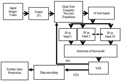
Figure 1. Block diagram of intra prediction coding
Figure 1 presents the block diagram of intra prediction coding performed in complex wavelet domain. The input video or image data is grouped into frames and each frame (F) is first encoded using intra frame coding. Within frames and between frames, the video coding model encompasses both spatial and temporal correlation between pixels, frames and objects. The input frame is divided into many sub units, each of which is predicted by the intra-frame prediction module and then subtracted from the actual sub unit. In the proposed method the frame is decomposed using DTCWT into complex wavelet sub bands and the subtraction residual is processed, the resulting output is quantized. To complete the compression of the input data, the modified output, expected units, and mode information, as well as the relevant header, are entropy encoded. The compressed data is decoded by the HEVC decoder at the receiver.
In the proposed method the frame is decomposed using DTCWT into complex wavelet sub bands. In this work we limit the decomposition to one level. One-level decomposition generates 16 sub bands that are grouped into two as real and imaginary sub bands. There are 8 real sub bands and 8 imaginary sub bands. Of the 8 sub bands 2 of them are low pass that contain intensity information of the original image and 6 of them are high pass that hold 6 directional orientations. Intra prediction is carried out on each of these 8 frames either considering real sub bands or imaginary sub bands. In this work, the real and imaginary sub bands are combined by taking magnitude of both. From the two low pass and six high pass sub bands intra prediction is carried out according to HEVC standards. The error (SAE) between the predicted sub bands and the actual sub bands are computed and the best mode of prediction is selected.
According to HEVC specifications, there are four macro blocks with block sizes ranging from 4 × 4 to 32 x 32, and each macro block has angular predictions in 33 directions, resulting in 132 different prediction modes [10]. This is done in the complex wavelet domain with all eight-sub bands.
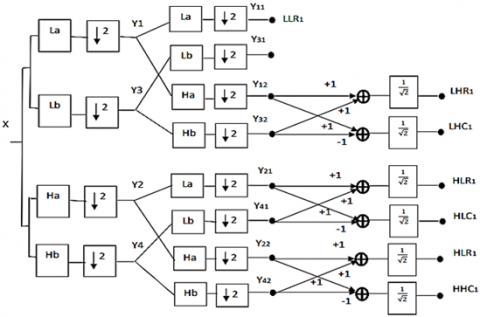
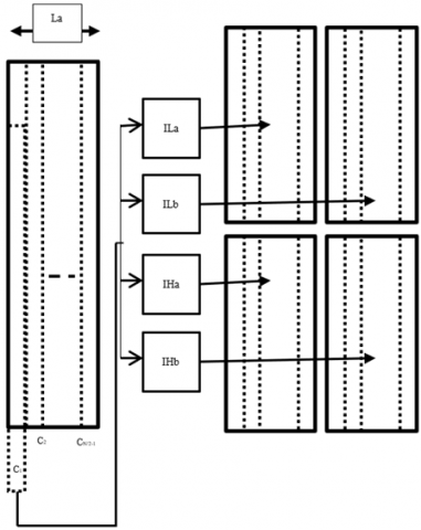
By increasing the sample rate by 2 in DWT at each level of both the real and imaginary tree, Kingsbury presented DTCWT to achieve shift invariance [6]. Down sampling by two in DWT causes aliasing, which is mitigated by using two trees (a and b) to process input data in parallel using four filters (La, Ha, Lb, Hb) with one sample offset between them. For each tree, two Hilbert transform pair mother wavelets are examined. The level 1 DTCWT structure for input picture X is shown in Figure 2. The row processing stage comes first, followed by the column processing stage.
Figure 2. Level-1 2D DTCWT structure
The first stage produces four outputs (y1, y2, y3, and y4), which are then processed to produce eight output bands (LLR1, LLC1, LHR1, LHC1, HLR1, HLC1, HHR1, and HHC1). Real and imaginary sub bands will be divided into four low pass and twelve high pass bands. The Daubechies 10-tap filter with orthonormal property is utilized in this study, as indicated in Table 1. The filter coefficients require 16-bit number representation, and they are scaled and rounded off to integer [11] to reduce the complexity of data path operation.
Table 1. Low pass and high pass filter coefficients (Real)
|
Order |
ILa |
IHa |
ILb |
IHb |
|
0 |
0 |
0 |
2 |
0 |
|
1 |
-22 |
-2 |
2 |
0 |
|
2 |
-22 |
2 |
-22 |
-22 |
|
3 |
178 |
22 |
22 |
-22 |
|
4 |
178 |
22 |
178 |
178 |
|
5 |
22 |
-178 |
178 |
-178 |
|
6 |
-22 |
178 |
22 |
22 |
|
7 |
2 |
-22 |
-22 |
22 |
|
8 |
2 |
-22 |
0 |
2 |
|
9 |
0 |
0 |
0 |
-2 |
To decompose the input image into DTCWT sub bands at level-1 the total number of filters required are 12 of which 6 are real and 6 of them are imaginary. The first stage of row decomposition requires 4 filters and each row is processed by the four filters to generate 1D-DTCWT output as shown in Figure 2.
Figure 3. Row processing in DTCWT
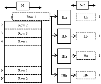
The filter coefficients are 10-tap, thus computing one output takes 10 multipliers and 9 adders for each row of N pixels, for a total of 10N and 9N multipliers and adders are required. For the first stage filtering as there are N rows and four filters the total number of multipliers and adders required are 40N2 and 36N2. Each of the rows processed generates output which is down sampled to length N/2. The outputs of each filter are denoted as La, Lb, Ha and Hb. The La and Lb are real and imaginary of components of low pass filters. Ha and Hb are the real and imaginary components of high pass filter output of DTCWT. Each of the row processed data is arranged as in Figure 3 by placing the low pass and high pass filets adjacent to each other. The real sub band and imaginary sub band after first stage decomposition divides the input image into two halves.
Figure 4. Arrangement of 1D-DTCWT output
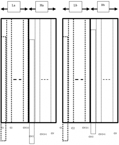
The column processing is carried out considering the rearranged 1D-DTCWT output in Figure 3. The data required for processing along the column is presented as in Figure 4. The column processing unit is shown in Figure 5. The elements of La from each of the row is read out column wise and is processed by the filter pair, similarly the rows of Ha are also read column wise and processed by another filter pair. The imaginary sub band generated in 1D-DTCWT is also processed by two pairs of DTCWT filters. In the second stage for column processing four pairs of DTCWT filters are used.
Figure 5. Data arrangement for column processing of 1D-DTCWT output
Figure 6. Column processing of 1D-DTCWT (real tree)
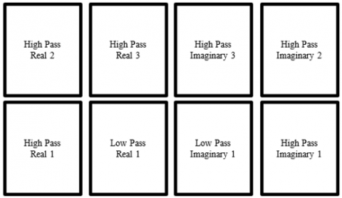
The column processing unit read N coefficients of 1D-DTCWT output along the column to generate N/2 output from each of the low pas and high pass filter and is arranged as in Figure 5. The real filter unit after simultaneously processing both La and Ha data along the column generates four sub bands each of size N/2. Similarly, the other three pair of filters generate the sub bands that are arranged as in Figure 6. After first level decomposition the 2D-DTCWT generates 8 sub bands of which two of them are low pass and six of them are high pass.
Compute the 8 sub bands of N x N image the total number of multipliers and adders are 80N2 and 64N2 respectively. In addition to the complexity of arithmetic operation the major design challenge is the data reading from the input register row wise or column wise and the latency in data processing between every frame. The total time required to compute the first component of all the N rows is N2 + N+10. Until this time the column processing will not be activated and in order to improve the latency in column processing unit parallel processing is carried out. The row processing is carried out on ten rows together using 10 different filters of low pass filter (Ha). Similarly, the first stage has 40 filters of La, Hb, Lb and Hb that process six rows simultaneously. The advantage of parallel processing is that if six rows are processed in parallel it generates the first components of 6 rows simultaneously at 10th clock cycle and from 11th clock onwards the column processing is initiated as column processing will have first 6 elements to compute. The latency is reduced from N2 + N+10 to 10 clock by enabling column processing to compute from 11th clock onwards. Only requirement is additional hardware (memory units and data processing units) are required. It is required optimize the delay and hardware complexity in processing ten rows in parallel. The row processing unit with parallel operation is presented in Figure 7. The parallel processing using ten low pass filters is mathematically expressed as in Eq. (1). The output is given as [Y6] = [H6][X6], where the ten rows of input represented as X6 is processed by ten filters with filter coefficients represented as H6 to generate ten rows of output represented by Y6.
$Y=\sum_{k=1}^{N} X_{k} H_{k}$ (1)
where,
The input data Xk is the image pixels.
The filter coefficients are represented as Hk.
Figure 7. Sub bands of 2D-DTCWT with level-1
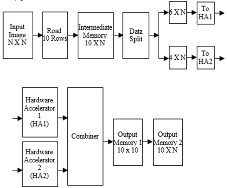
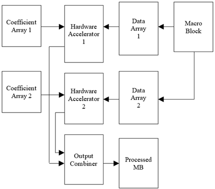
In order to have a trade-off between computation complexity and latency systolic array based architecture is designed for DTCWT computation. Design of optimum structure for systolic array algorithm is presented in this section considering an input data X6 of size [6 x 10]. The systolic array structure for input X6 and to generate output Y6 of size [6 x 10] using systolic array logic requires the coefficient H6 data size to be [10 x 10]. The total number of processing elements in the systolic array structure will be 100 elements and the latency will be 10 clock cycles. In order to achieve trade-off between latency and area utilization a new method is presented in this work. In the proposed work shown in Figure 8 from the input image of size N x N, first 6 rows are read into intermediate memory and the first block of [6 x N] elements is split into [6 x N] and [4 x N] data groups. The Hardware Accelerator 1 (HA1) processes the first 6 x 6 data of 6 x N and Hardware Accelerator 2 (HA2) processes the second data of 4 x 4 of 4 x N to generate the 1D-DTCWT coefficients independently. The combining unit which is a adder unit accumulates the output of HA1 and HA2 to generate the Y6 output and is stored in the output register 1. The next set of data is read into, until all the N elements of the first 6 rows are processed. The final output is stored in the output register 2, and the next 6 rows are read into the unit for processing.
The advantage of the proposed data split and data processing using systolic array structure is that the number of processing elements required are 52 (the 6 x 6 array requires 36 and the 4 x 4 array requires 16). The hardware complexity is reduced by 48% as compared with direct implementation. There will be additional delay of one clock cycle due to the combining unit and additional overhead with use of adder logic. Figure 9 presents the proposed data processing scheme.
Figure 8. Parallel processing of six rows for 1D-DTCWT decomposition
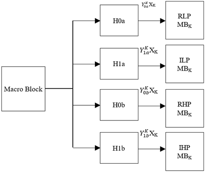
The N x N image is grouped into Tm number of tiles with each tile comprising of 6 x N rows. Each of the 6 x N rows or the tile is further divided into macro blocks (MB) each of size 6 x 10. Each of the MBs is processed by the systolic array structure with the data split processing structure. As there are 4 filter in the first stage each macro block is processed by the four filters (as shown in Figure 10) to generate the outputs {RLP, ILP, RHP, IHP} that represents real (R) and imaginary (I) low pass (LP) and high pass (HP) DTCWT coefficients.
Each of the filter is designed to process the [6 x 10] input data by splitting the data into [6 x 6] and [6 x 4]. The HA1 is designed to perform data processing of X= [6 x 6] and H = [6 x6] to generate output of Y of [6 x 6]. The HA2 performs data processing of X= [6 x 4] and H = [4 x 4] to generate output of Y of [6 x 4]. The output combiner having array adders of 6 accumulates the output of HA1 and HA2 to generate the final output Y of size [6 x 10]. The proposed data split data processing structure is presented in Figure 11.
Considering the output Y00 the first output is expressed as in Eq. (2),
Y00=h00aX00+h10aX01+h20aX02+h30aX03+h40aX04+h50aX05+h60aX06+h70aX07+h80aX08+h90aX09 (2)
The expression is split into two section as Y0M0 and Y0L0 as in Eq. (3) that represents the MSB term and LSB term respectively,
Y00M=h00aX00+h10aX01+h20aX02+h30aX03+h40aX04+h50aX05 (3a)
Y00L =h60aX06+h70aX07+h80aX08+h90aX09 (3b)
Figure 9. Proposed data path unit for row processing of DTCWT filter
Figure 10. Row data processing using proposed parallel scheme
Figure 11. Macro block processing
The HA1 and HA2 compute the two outputs independently and the output is accumulated by the combiner unit as in Eq. (4).
Y00=Y00M+Y00L (4)
The processing element to perform the operation of Eq. (3) and Eq. (4) is presented in Figure 12. The processing element comprises of two units labeled Processing Element MSB (PEM) and Processing Element LSB (PEL) that computes the operations as indicated in Eq. 3(a) and 3(b) independently considering the filter coefficients Hm0a and Hl0a. The outputs are accumulated in the adder stage to generate the final output Y00.
Figure 12. Data split data processing unit
Each of the PEM and PEL comprises of a Multiply and Accumulate Unit (MAC) that performs multiplication and accumulation operation on the inputs and filter coefficients.
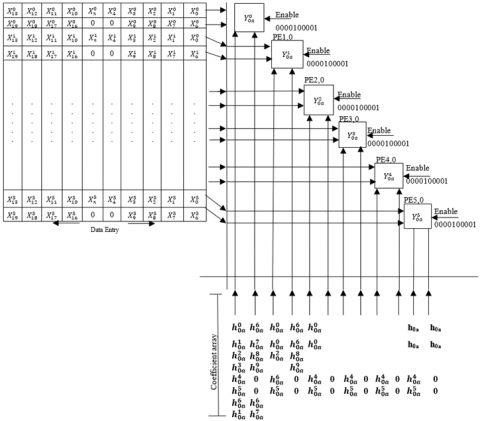
Considering the processing element the parallel row processing unit structure is designed and is presented in Figure 13. The processing elements PE0,0 to PE5,0 are arranged in a column with each processing elements having four inputs of which two inputs are for the data input and two for the coefficients input.
Figure 13. Data processing unit (Processing element) for computing Y00
In addition to these four inputs the Enable input is also included to control the data flow and perform data combining operation. The data input of every row is split into two sections the first input has 6 data samples. For example, for PE0,0 the first data input is from first row represented by {X00, X01, X02, … X05} and the second data input is represented by {X06, X07, X08, X09, 0, 0}. The second input is preceded by two zeros to synchronize the data combining operation. The filter coefficients for the PE0,0 is split into two sections as {h00a, h10a, h20a, h30a, …, h50a} and the second input is {h60a, h70a, h80a, h90a, 0, 0}. Similarly for all the processing elements from PE1,0 to PE5,0 the six rows of data and the filter coefficients are split into two sections and is fed into the systolic array structure. The combiner or the accumulator (ACC) accumulates the six products of both PEM and PEL. The enable data E is set with control input {0,0,0,0,0,0,1} to enable the output register Ra to store the accumulated output after ACC computes the final output after 6 clocks.
The proposed structure comprises of six processing elements with each processing element having two MAC units for computing Y00M and Y00L. The first output of every processing element is generated at the end of 10th clock cycle and hence the latency is 10 clock cycle and throughput are 6 outputs per clock. The total number of multipliers and adders required are 12, 18 respectively. The intermediate registers required to store the data are 24. Figure 14 presents the proposed systolic array structure for first stage filtering using parallel processing structure presented in Figure 13.
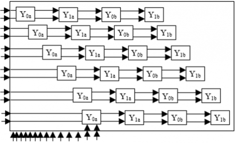
The first stage processing unit shown in Figure 15 comprises of four filters and with parallel row processing logic proposed in this work, 6 x 4 systolic array structure is designed with each of the processing elements computing the filter output for all six rows simultaneously. The first filter output (Yn0a) is generated at the end of 10 clock cycles, the second filter output (Yn1a) is generated after 11th clock cycle and the fourth filter output (Yn1b) is generated at 13th clock cycle.
Figure 14. Systolic array structure for parallel processing of six rows
Figure 15. First stage processing unit
The throughput is 24 outputs per clock cycle. The total number of multipliers and adders are 48 and 72 respectively. With additional overhead of multipliers and adders the throughput of the proposed structure is increased by 24 outputs per clock. Based on the design aspects presented the overall system for computing level-1 2D-DTCWT is designed. The top level architecture for the 2D-DTCTW is presented in Figure 16. For analysis of the proposed structure and verify its functionality a test image of size 16 x 16 is considered. Symmetric extension is carried out to ensure there is no loss of data at the boundary and image is extended to 18 x 18 by padding with the pixels in the boundary. The input data is read row wise and every iteration 6 rows are read into the design. The 6 x 18 data is processed by the both row processing unit and the column processing unit. Three tiles of data is read into and processing is carried out to generate the 2D DTCWT sub bands. The final output of 8 sub bands is generated.
The primary building blocks of the 2D-DTCWT process are the row processor (1 unit) and column processor (4 units). As the row processing and column processing perform the tasks of data processing with different set of filter coefficients, the row processor and column processor perform similar task. For estimating the hardware implementation performances, the row processor is modelled in Verilog HDL and is verified for its functionality. The functional correct model is implemented in ASIC considering 45nm CMOS technology. The reports generated and analyzed for area, timing and power performances.
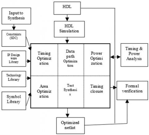
Logic synthesis is the process of converting a design description written in a hardware description language such as Verilog into an optimized gate-level netlist mapped to a specific technology library. Cadence environment is used for Logical Synthesis, considering 45nm CMOS technology (GPDK). Both the Design Rule Constraints and Optimization constraints are applied. The target and the like library chosen, the technology libraries contain the information about the characteristics and functions of each cell. Logic library contain the information about the library group, library level attributes, environment description. The Design Rule Constraints are applied to the design using the Technology Library. The Optimization Constraints are defined by the designer. Timing constraints, Maximum area, and Minimum porosity are the different optimization constraints. Timing Constraints are given the highest priority and is the one used for optimization in this design. Figure 16 presents the synthesis flow diagram adopted for designed DTCWT and IDTCWT.
Figure 16. Top level block diagram of 2D DTCWT processor
Figure 17. ASIC synthesis flow diagram
In addition to the setup and hold analysis, the STA signoff tool performs recovery, removal, gate setup, gate hold and min pulse width checks. The physical design methodology or the flow is explained and the implementation of DWT and IDWT in terms of physical design. The physical design tool from Cadence is used. Attempts have been made to produce a DRC clean optimized design along with the desired timing. Figure 17 presents the physical design process adopted for generating GDSII for DTCWT and IDTCWT. From the front end and physical design flow the synthesis report is generated and the hierarchy in the cells and sub systems in the design is mapped in Figure 18. In order to build the optimum synthesis netlist for the proposed model it is required to set the constraints appropriately.
Figure 18. Physical design flow
From the front end and physical design flow the synthesis report is generated and the hierarchy in the cells and sub systems in the design is mapped in Figure 18. In order to build the optimum synthesis netlist for the proposed model it is required to set the constraints appropriately. In this work timing constraints have been given highest priority and four clock periods are set to generate synthesis reports. From the synthesis results the netlist is of 9 to 10 hierarchies and each hierarchy comprises of minimum of 6 references. Optimizing the hierarchy to less than 9 levels has led to failures in meeting timing constraints. The estimated netlist meeting timing requirements during the front end synthesis process will be further constrained during physical synthesis process.
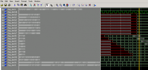
A well-known test vector is chosen to check the outcomes of the DTCWT algorithm. Theoretical values of the actual output are derived for a known set of test inputs and compared to simulation results output. As test inputs, the results of the 1D-DTCWT processor for a known set of inputs in the range of 0 to 255 were employed, and the associated outputs were generated using ModelSim. Figure 19 shows the design hierarchy and the test results are shown in Figure 20, considering the real part of DTCWT and are represented as variable name “top_DWT”. The 1D-DTCWT generates both real and imaginary data and to verify the functionality only the real data is considered. From the simulation results it is found that the 1D-DTCWT processor results are matching the theoretical requirements.
A well-known test vector is chosen to check the outcomes of the DTCWT algorithm. Theoretical values of the actual output are derived for a specified set of test inputs and compared to simulation output produced Figure 19.
The 1D-DTCWT As test inputs, the results of a known set of inputs in the range of 0 to 255 were employed, and the corresponding outputs were obtained using ModelSim. The test results are presented in Figure 20, considering the real part of DTCWT and are represented as variable name “top_DWT”. The 1D-DTCWT generates both real and imaginary data and to verify the functionality only the real data is considered. From the simulation results it is found that the 1D-DTCWT processor results are matching the theoretical requirements.
Figure 19. Design hierarchy
Figure 20. First stage of 1D DTCWT processor simulation results using ModelSim
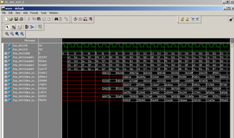
Figure 21 illustrates the simulation results of a 2D DTCWT processor, which shows 8 levels of subband data at the output from 16 × 16 inputs.
Figure 21. 2D DTCWT of frame1 Simulation results
The design has been synthesized in the Cadence environment, and also post placement, map, and route simulation. The initial estimation of area performances for the four different timing constraints is summarized in the Table 2 shown below.
Table 2. Area estimates comparison for four different timing constraints
|
Parameters |
Clock 1 |
Clock 2 |
Clock 5 |
Clock 7 |
|
Logic Area(sq.mm) |
31116.528 (79.9%) |
33550.200 (80.3%) |
20413.980 (83%) |
15843.150 (83%) |
|
Sequential Area(sq.mm) |
3640.932 (9.4%) |
3500.370 (8.4%) |
2942.910 (12%) |
2724.372 (14.3%) |
|
Total instances |
11043 |
11871 |
7427 |
5765 |
|
Total Area(sq.mm) |
38927.124 |
41804.028 |
24583.302 |
19086.336 |
From the initial estimate it is identified that with clock 7 the total area is reduced by a factor of 54% as compared with clock 2 constraints. The number of instances required for the design is limited to 5765 as compared with initial estimate of 11871. The logic cells and the sequential cell area is also reduced as the number of instances are also being reduced with changes in clock constraints. From this initial analysis it is required to further analyze the area, power and speed performances by carrying out physical design process.
6.1 Physical design implementation
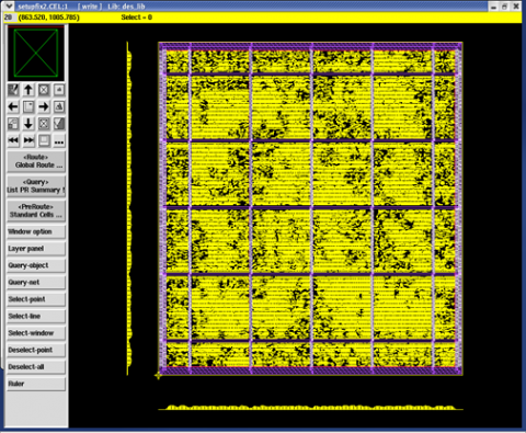
Floor planning is carried out with core utilization ratio of 80%, aspect ratio of 1, rows flipped, double backed design with channel less scheme. The Top Design File (TDF) is prepared for placement of pins. Figure 22 presents the floor planning of the design. Placement & Routing (P&R) is carried out and the initial area utilization report is generated. The “unit” tile covers 44.36% of core area while invoking low power tile “lp_unit” the core area utilization is 65.53%.
Figure 22. Different unit tile placement
Considering block level scheme the power planning design is carried out and the core ring width is calculated as follows:
Total Power Consumed = 4.6 mW
Power Per Side = 4.6 mW/4 = 1.15 mW
Current Per Side = 1.15 mW/ Vdd = 1.15 mW/0.8V= 1.4375 mA
Core Power Ring Width = (1.4375 mA/Current Density of Metal)* 100 nm = (1.4375 mA/0.58mA)* 100 nm= 247.89 nm =~ 250 nm
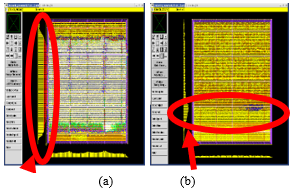
Thus the core power ring width is kept as 250 nm. The straps are given a width of 50 nm. Based on power planning design congestion map is estimated. The congestion map is shown in Figure 22 for two different parameters.
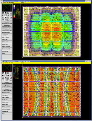
With a floor planning aspect ratio of 1 and a core usage of 70%, Figure 23 on the left is generated. Over the limited value of one, horizontal congestion is observed (represented by the arrow) throughout the core area. By specifying height and width in the design, the core area must be increased. The other congestion map (figure right) is generated using a floor layout with a 3000 nm core area. Although the congestion in the core area has decreased, the area where two different unit tiles merge, as indicated by the circle, remains a source of concern. But design can be routable and can be carried to next stages of place and route flow provided timing is met in subsequent implementation steps. Varying the core width and height the congestion map is optimized and is presented in Figure 24 and the core utilization of the design is estimated to be 62.08%. It is observed that the congestion is normalized in the optimum design.
Figure 23. Congestion maps of multi height implementation
Figure 24. Congestion map for common cell height implementation
IR drop map is generated for the design with optimum congestion and the IR drop map is presented in Figure 25. Highest IR drop is of 18 mV which is found at centre of the core area highlighted with red color and is within the acceptable limits of < 20 mV. EM violation map is generated and presented in Figure 23 (b) the violations are highlighted in red color around the each strap. By varying the parameters power planning such as increasing the width of straps and introducing slots in the global power rings the violations are minimized.
Figure 25. EM violation map and IR drop map
Considering the analysis carried out the final design is generated and GDSII is file is prepared. The clock frequency (clock period) of the design is varied from 1 ns to 7 ns. For each of the clock settings the area, timing and power is estimated form the reports generated meeting all the requirements. Table 3 summarizes the power dissipation report for four different constraints. The total area in Sq. mm is identified to be 25966 and is reduced by a factor of 51%. The initial estimate of the area was 19086.336 sq. mm which is increased by factor of 26%. This increase is due to the placement of addition cells in the design to meet the area and power constraints. The dynamic power dissipation of the optimum netlist is reduced by a factor of 82% and the leakage power is reduced by 72%. Table 4 presents the improvement in area, timing and power performances. From the power dissipation report it is observed that setting appropriate timing constraints impacts the system performances. Clock period of 5 ns and 7 ns provide slack of 0 and hence is considered as optimum design setting.
Table 4 presents the details of the critical path in the netlist for four different clock constraints set in the design to obtain the netlist. The critical path from cnt1 to out_reg [1] is offers a maximum delay of 347 ps, this critical path is shifted to mc2 to q_reg with timing constraint of clock 7. The critical path delay in clock 7 settings is 317 ps which is the minimum of all the four critical paths identified.
From the timing report analysis, it is observed that with change in clock constraints the critical path also changes its metrics. Identifying the critical paths and its metrics also assists in deciding proper timing constraints for design optimization.
Table 3. Presents the summary of the design in terms of area, power and speed performances
|
Report |
T=1ns |
T=2ns |
T=5ns |
T=7ns |
|
Area (sq.mm) |
50423 |
53928 |
33156 |
25966 |
|
Cells |
11043 |
11871 |
7427 |
5765 |
|
Total Power(nW) |
4649834.517 |
14531450.72 |
4103695.745 |
2576115.260 |
|
Dynamic power(nw) |
4647562.044 |
14528930.66 |
4102606.710 |
2575418.910 |
|
Leakage power(nw) |
2272.473 |
2520.057 |
1089.035 |
696.350 |
|
Setup Timing |
89 |
99 |
132 |
141 |
|
Slack(ps) |
-2614 |
-1620 |
0 |
0 |
Table 4. Critical paths of the netlist
|
Clock |
Timing point |
Delay(ps) |
|
Clock 1 |
cnt1/out_ reg [1]/Q |
347 |
|
Clock 2 |
cnt1/out_ reg [2]/Q |
344 |
|
Clock 5 |
mc5/rg2/d10/q_ reg/Q |
357 |
|
Clock 7 |
mc2/rg3/d7/q_ reg/Q |
317 |
Hardware efficient DTCWT architecture for intra prediction coding that is designed suing systolic array algorithm is presented in this work. Parallel processing of the input images considering multiple rows and columns is designed to accelerate the throughput. The systolic array structure design presented in this work is for multiplying matrix of 6 x 6 and 6 x 4 elements. The data control unit provides synchronization of information flow in both the SAA structures. The HDL code is developed and verified for tis functionality and is synthesized in CMOS technology. RTL to GDSII flow is carried out to generate the optimum timing, area and power report. From the reports generated the design is optimized for tis performances with timing being considered as highest priority. The maximum operating frequency is identified to be of 300 MHz and the power dissipation is limited to less than 3 mW at 2.0 V power. Further optimization in the design metrics can be achieved by increasing the number of frames to be processed.
I would like to express my special thanks of gratitude to the Management, Principal and Head of the Department of S V Engineering College, Tirupati, AP, India who gave me the opportunity to do this research work.
[1] Wang, Y., Ostermann, J., Zhang, Y.Q. (2002). Video processing and communications (Vol. 1). Upper Saddle River, NJ: Prentice hall.
[2] Sullivan, G.J., Ohm, J.R., Han, W.J., Wiegand, T. (2012). Overview of the high efficiency video coding (HEVC) standard. IEEE Transactions on Circuits and Systems for Video Technology, 22(12): 1649-1668. https://doi.org/10.1109/TCSVT.2012.2221191
[3] Kim, I.K., Min, J., Lee, T., Han, W.J., Park, J. (2012). Block partitioning structure in the HEVC standard. IEEE Transactions on Circuits and Systems for Video Technology, 22(12): 1697-1706. https://doi.org/10.1109/TCSVT.2012.2223011
[4] Richardson, I.E. (2011). The H. 264 Advanced Video Compression Standard. John Wiley & Sons. https://patents.justia.com/patent/10602187.
[5] Kingsbury, N.G. (1999). Image processing with complex wavelets. Philosophical Transactions of the Royal Society London A, 357(1760): 2543-2560.
[6] Selesnick, I.W., Baraniuk, R.G., Kingsbury, N.C. (2005). The dual-tree complex wavelet transform. IEEE Signal Processing Magazine, 22(6): 123-151. https://doi.org/10.1109/MSP.2005.1550194
[7] Madhurima, V.,Padmapriya, K. (2022). HEVC encoding and decoding using fast algorithm for intra frame partition-prediction using DTCWT. In Micro-Electronics and Telecommunication Engineering, 759-773. https://doi.org/10.1007/978-981-16-8721-1_69
[8] Divakara, S.S., Patilkulkarni, S., Raj, C.P. (2018). High speed area optimized hybrid da architecture for 2d-dtcwt. International Journal of Image and Graphics, 18(1): 1850004. https://doi.org/10.1142/S0219467818500043
[9] Lainema, J., Bossen, F., Han, W.J., Min, J., Ugur, K. (2012). Intra coding of the HEVC standard. IEEE Transactions on Circuits and Systems for Video Technology, 22(12): 1792-1801. https://doi.org/10.1109/TCSVT.2012.2221525
[10] Madhurima, V., Padmapriya, K. (2021). FPGA Implementation of High Speed Distributed Arithmetic Optimum Memory Utilized DTCWT Architecture for Image Processing. Design Engineering, ISSN 0011-9342, 6: 1331-1346.
[11] http://www.thedesignengineering.com/index.php/DE/article/view/2119.