Haider Al-Mumen![]()
© 2024 The author. This article is published by IIETA and is licensed under the CC BY 4.0 license (http://creativecommons.org/licenses/by/4.0/).
OPEN ACCESS
In this paper, a tactile sensor based on ZnO nanorods was fabricated and characterized. A silicon and a polyamide substrate were utilized to achieve both a rigid and a flexible sensor. The ZnO nanorods was achieved using hydrothermal technique. The size and shape of the nanorods were recognized by the Scanning Electron Microscope (SEM). An interesting hexagonal cross section shape were achieved, which is very sensitive to the external pressure. An elevation in the detector output current was measured as the pressure applied to the detector. Two tests were applied to the sensor, first, a horizontal pressure and second, a bending pressure with several bending angles. The time response was graphed for both cases. Furthermore, the effect of oxygen plasma on the nanorods structure was analyzed by the SEM, Raman spectroscope and nanometer.
nanorods, touch sensor, flexible, ZnO, piezoelectric
The world of nanotechnology has witnessed a great development, especially in the field of nano sensors, nanomaterials, and nanodevices fabrication [1-6]. ZnO nanorod is a stunning nanomaterial, which is a promising to be the building block for the electronic devices and sensors. This is due to its semiconductor properties and wide bandgap [6, 7]. Several electronic devices based on ZnO nanorods were reported. For example, it has been used as a photosensor [8], taking advantage of the large surface area of the nanorod. The nanorods photosensors have been constructed, specifically, ultraviolet photosensors and have been proven to have high sensitivity as well as high response time. Zinc oxide nanorods were also fabricated to be a light emitting diode [9, 10] instead of the conventional designs that made of semiconductors, taking advantage of the cheapness, ease of the manufacturing process in addition to its large band gap. The focus was on manufacturing photodiodes with short wavelengths, such as laser diodes.
Furthermore, due to its stunning electronic properties, some research groups have succeeded in fabrication of FET transistor that made of ZnO nanorods. The success in manufacturing such kind of transistors probably opens the path for more complicated electronic devices such as logic gates and digital memory [11, 12]. Moreover, Tactile nanorods sensor [13, 14] is one of the hottest applications because piezoelectricity is one of the most significant properties of the ZnO. This means that such kind of nano material has both mechanical and electrical properties that the material reacts to. Theoretically, when a pressure applied to the nanorods, the surface would be deformed. This deformation causes movement in the charge carriers through material. This phenomenon displays the ability of building a self- powered sensor. Since the ZnO nanorods surface have the ability to withstand a huge subjected pressure, therefore, it can be easily used in fabrication of flexible sensors.
In this work, the ZnO nanorods were grown on a silicon substrate, the nanorods were studied under the SEM and also under Raman Spectroscope to display the hexagonal shape, the surface profile, and the effect of the plasma on the surface profile and crystal structure. Then a flexible sensor based on ZnO nanorod was fabricated on a polyamide (flexible) substrate and tested under vertical pressure and bending pressure.
Figure 1. Sample preparation in the lab
The sample preparation requires cleaning the substrate, as it is very significant issue in the growing process of the nanorods. Any kind of contamination on the surface of the substrate can produce unexpected results, specifically, the nanorods shape which affects the sensing property. The process of cleaning the substrate begins by rinsing with acetone, isopropanol and then deionized water. Hydrothermal technique was used to produce nanorods [15, 16]. Briefly, a seed layer of 1.835 g Zinc acetate was mixed with 1000 ml of ethanol and then spin coated about 1000 rpm for 1 min on the substrate, then baked at 100℃ for 10 min. This process was repeated 3 times. Basically, the seed layer decides the quality of the ZnO nanorods that will grow in the next fabrication process. 0.87 g of nitrate hexahydrate was mixed with 0.44 g of hexamethylenetetramine and then added to 30 ml deionized water. After that, the substrate was immersed in a battle and placed in the oven at 70℃ for around 4 hours (as shown in Figure 1).
Two types of substrates were used, silicon dioxide on silicon, which is a rigid substrate, and polyamide substrate, which is a flexible substrate.
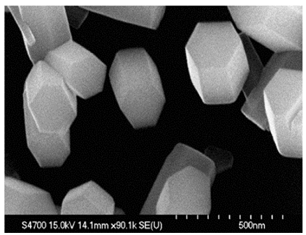
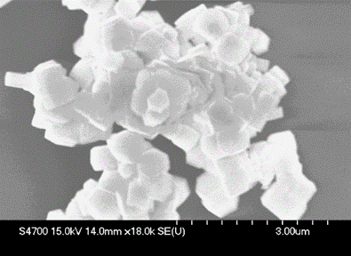
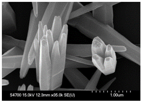
SEM was used for imaging the ZnO nanorods. Several magnification factors were used to determine the shape of the nanorods. Based on the lab experiments, the dimensions and shape are depending on the seed layer and the growing time. Figure 2 illustrates several shapes and size of the archived nanorods structures. Obviously, the cross-sectional area is a hexagonal shape, some with one head and some with multihead, this is depending on the growing process, in terms of chemical concentrations, growing time and also the seed layer. In fact, the seed layer is very significant process step as it decides the quality and shape of the nanorods.
(a) Single head at X90k
(b) Multihead at X35K
(c) nanorods grid at X2.0K
(d) A sample with no seed at growing process
Figure 2. ZnO nanorods under SEM
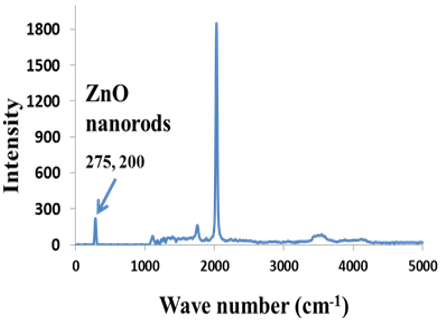
To prove the availability of the ZnO material in the sample, Raman spectroscope instrument was used. This instrument is non-distractive instrument that can identify what kind of molecules deposited in the sample. It also gives an indication about the crystal structure of the material, meaning that one can determine whether a surface of a material is defective or not [17-19].
A sample of nanorods was prepared on silicon dioxide over silicon substrate and checked under Raman spectroscope, as shown in Figure 3. The peak at wave number of 275 cm-1 indicates the foundation of the ZnO nanorods. The peak intensity which is unitless, is 200.
Figure 3. Raman spectrum of the of the ZnO nanorods
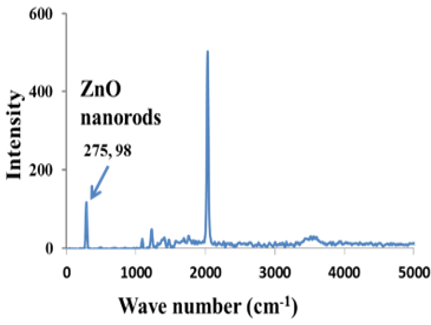
Many reported articles claimed the impact of the plasma on the crystal structure and surface roughness of nanomaterials [20]. They found that the surface roughness increases the sensitivity of the ZnO gas senor [21]. Indeed, Raman spectroscope is an excellent instrument for studying the surface roughness, as it is non-destructive tool that can be used to detect the surface defects of several materials including nanomaterials. Wave number, the inverse of the wavelength is usually measured to decide the kind of material under test. This number also called Raman shift, as it represents the difference between the incoming laser light to the reflected one from the sample surface. The prepared sample was checked by Raman spectroscope after and before subjecting to the O2 plasma of 300W for 3 mins. The sample was also checked by SEM after and before subjecting the O2 plasma (Figure 4). It was observed that the intensity peak at 275 (Figure 4a), which is the fingerprint of the ZnO nanorods, decreases significantly after plasma exposure, particularly, from 200 to 98 (Figure 4b and 4c). A huge surface roughness and crystal distractive were seen under SEM (Figure 4d and 4f). The surface roughness increases with the increasing of the plasma exposure time and exposure power. Based on the reported articles [14, 22-24], treatment with plasma enhances the surface absorption to some gases, such as carbon monoxide, methane, and hydrogen. However, for sensing mechanical pressure (piezoelectricity), the sensitivity was significantly decreased due to crystal disorder of the nanorods by the plasma exposure (as would see in the next section).
(a) Raman spectrum before plasma exposure
(b) Raman spectrum after plasma exposure
(c) comparison between the intensity peaks, inset is the plasma instrument during exposure
(d) SEM image before plasma exposure at magnification at magnification at magnification of X35K
(e) Raman spectrum of the ZnO nanorods after short (dark color) and long (light color) exposure time
(f) The SEM images after plasma exposure at magnification at magnification at magnification at magnification of X40K
Figure 4. Effect of plasma on the ZnO nanorods
The photolithography method was used. The sample was initially cleaned using acetone, isopropanol, and deionized water and dried with nitrogen. Then, a layer of copper with a thickness of 3000 angstroms was deposited on the surface of the polyamide using a Thermal Evaporator device under a pressure of 1×10⁻⁶ Torr. The sample was then coated with a layer of photoresist with a thickness of 1 micrometer using a spin-coating device. The sample was then placed on a hot plate for three minutes at a temperature of 100℃ to dry it by evaporating the solvent. The sample was then exposed to ultraviolet radiation with a wavelength of 365 nanometers for 2 minutes, of course, through a mask. Then, the sample was placed in the developer to display the pattern. Finally, the sample was placed in iron chloride salt to dissolve the copper in areas that are not covered by photoresist. The sample was then washed with water and dried with nitrogen. Finally, the remaining photoresist was removed with acetone. A layer of zinc oxide nanorod was grown on the surface of the substrate as described in the previous section.
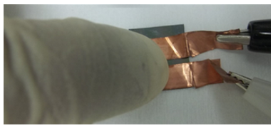
One of the important properties of nanorods is its ability to withstand the external pressure and deformation [25]. The reaction of the nanorods sample is generating an electric current due to nano piezoelectricity. Theoretically, at no pressure, dipoles that are created due to the zinc and oxygen ions are not arranged in a regular form but fixed in a place with no movement, this leads to no piezoelectric effect and then no current flows. When the ZnO nanorods is subjected to external pressure, the nanorods are deformed and then the piezoelectric effect appears. During pressure, the electrons would move from one electrode to another until the saturation reached, meaning that current will not increase anymore. To implement this practically, the nanorods were grown on a flexible substrate, a polyamide substrate. First, the sample was subjected to a variable external pressure by index finger, roughly a force of 10 to 40 N, starting relatively from low pressure to relatively high pressure (Figure 5). As a result, different electric current values from 0 nA, at no pressure to 10 nA at relatively max pressure, were obtained, with neither bias voltage nor amplification. The current was measured through two copper electrodes, which are connected to the 41,458-semiconductor parameter analyzer. Basically, the generated current comes from the fact that when a vertical or bending force is applied to the nanorods a mechanical stain due to compression and stretching will be occurred. Then, a potential difference will be generated because of the charge carriers movement on the surface of the nanorods. This effect is called nano piezoresistivity.
(a) Schematic representation
(b) experimental setup
(c) The device time response
Figure 5. Exposing the sample to external pressure
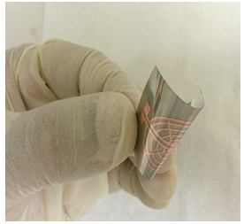
The second test applied to the sample is the bending test. As mentioned, the substrate is a polyamide, which is flexible. As shown in Figure 6, the sample was subjected to bending pressure with ranging angles from 180 (no bending) to about 45 degrees. This has led to elevations in the current level from 5nA to 15 nA, which is proportional to the bending angle. The current saturates at a particular value of applied force. Also, the current- pressure relationship is linear.
(a) photographic image of the device
(b) The bending angle between 180 (no bending) to about 45 degrees
(c) bending angle versus generated current
Figure 6. Bending stress effect on ZnO nanorods grown on a flexible polyamide substrate
The device was also tested in response to a mechanical touch (press and release), after and before plasma exposure (Figure 7). Result showed a negligible response to external pressure compared to case before plasma exposure test. As displayed in the inset of Figure 7, the crystal structure was destroyed and the piezoelectric effect was disappeared.
Figure 7. The device time response before and after plasma exposure. Inset is the SEM image of the nanorods before and after exposure at magnification at magnification of X90K
This work represents a practical study of the ZnO nanorods as pressure and touch sensors. Several devices were designed, fabricated and, tested. The ZnO nanorods are grown using the conventional hydrothermal technique. SEM images show a stunning shaped of the nanorods in the nanoscale size, particularly the hexagonal cross section of the nanorods. Moreover, the effect of the oxygen plasma on the crystal structure was also studied by using Raman spectroscope. The electrical test for the samples were done on both rigid and flexible substrates. Remarkable elevation in current was observed due to applied force (vertical and bending forces); this can be attributed to the piezoresistive property of the nanorods, which probably open the door for the practical powerless sensors design. On the other hand, unlike nanorod based-gas or chemical sensors, the plasma causes significant decrease in the sensor sensitivity. This kind of sensors open the door for a lot of practical applications such as tactile sensors particularly in the field of health care, robotics. Furthermore, since the sensor is self-powered, it can be used in portable devices.
[1] Kadhim, H.J., Al-Mumen, H., Nahi, H.H., Hamidi, S.M. (2022). Tunable plasmon induced transparency in one-dimensional gold nano-grating as a new kind of neuro-transmitter sensor. Optik, 269: 169907. https://doi.org/10.1016/j.ijleo.2022.169907
[2] Rao, F.B., Almumen, H., Dong, L.X., Li, W. (2011). Highly sensitive bilayer structured graphene sensor. In 2011 16th International Solid-State Sensors, Actuators and Microsystems Conference, Beijing, China, pp. 2738-2741. https://doi.org/10.1109/TRANSDUCERS.2011.5969828
[3] Al-Mumen, H., Rao, F., Dong, L., Li, W. (2012). Characterization of surface heat convection of bilayer graphene. In 2012 12th IEEE International Conference on Nanotechnology (IEEE-NANO), Birmingham, UK, pp. 1-4. https://doi.org/10.1109/NANO.2012.6322100
[4] Eisa, Z., Al-Mumen, H. (2022). Characteristic control of SWCNT-FET by varying its chirality and dimensions. Indonesian Journal of Electrical Engineering and Informatics (IJEEI), 10(3): 698-706. http://doi.org/10.52549/ijeei.v10i3.4046
[5] Al-Mumen, H., Hamad, A.A. (2022). Design and characterization of an radio frequency reused energy system for nano-devices. Bulletin of Electrical Engineering and Informatics, 11(5): 2595-2602. https://doi.org/10.11591/eei.v11i5.4321
[6] Vu Anh, T., Pham, T.A.T., Mac, V.H., Nguyen, T.H. (2021). Facile controlling of the physical properties of zinc oxide and its application to enhanced photocatalysis. Journal of Analytical Methods in Chemistry, 2021(1): 5533734. https://doi.org/10.1155/2021/5533734
[7] Sáenz-Trevizo, A., Amézaga-Madrid, P., Pizá-Ruiz, P., Antúnez-Flores, W., Miki-Yoshida, M. (2016). Optical band gap estimation of ZnO nanorods. Materials Research, 19: 33-38. https://doi.org/10.1590/1980-5373-MR-2015-0612
[8] Zhang, Q.P., Xie, G.Z., Duan, M.Y., Liu, Y.T., Cai, Y.L., Xu, M., Zao, K., Tai, H.L., Jiang, Y.D., Su, Y.J. (2023). Zinc oxide nanorods for light-activated gas sensing and photocatalytic applications. ACS Applied Nano Materials, 6(19): 17445-17456. https://doi.org/10.1021/acsanm.3c02403
[9] Zeng, J., Qi, Y., Liu, Y., Chen, D., Ye, Z., Jin, Y. (2022). ZnO-based electron-transporting layers for perovskite light-emitting diodes: Controlling the interfacial reactions. The Journal of Physical Chemistry Letters, 13(2): 694-703. https://doi.org/10.1021/acs.jpclett.1c04117
[10] Li, R.Q., Fu, J.W., An, J.X., Wang, Y.Z., Lu, W.J., Chen, Y.H., Lou, H., Wang, S., Lai, W.Y., Zhang, X.W., Huang, W. (2021). Highly efficient inverted organic light-emitting diodes adopting a self-assembled modification layer. ACS Applied Materials & Interfaces, 13(35): 41818-41825. https://doi.org/10.1021/acsami.1c08890
[11] Kim, E.B., Imran, M., Lee, E.H., Akhtar, M.S., Ameen, S. (2022). Multiple ions detection by field-effect transistor sensors based on ZnO@ GO and ZnO@ rGO nanomaterials: Application to trace detection of Cr (III) and Cu (II). Chemosphere, 286: 131695. https://doi.org/10.1016/j.chemosphere.2021.131695
[12] Navaneetha, A., Prasad, D., Deepthi, S.A., Reddy, A.K., Chandhra, A.J., Panigrahy, A.K. (2023). Analysis of nanowire FET over FinFET. In 4th International Conference on Advancements in Aeromechanical Materials for Manufacturing (ICAAMM-2021), Hyderabad, India, Vol. 2492, No. 1. AIP Publishing. https://doi.org/10.1063/12.0012455
[13] Dong, B., Shi, Q., Yang, Y., Wen, F., Zhang, Z., Lee, C. (2021). Technology evolution from self-powered sensors to AIoT enabled smart homes. Nano Energy, 79: 105414. https://doi.org/10.1016/j.nanoen.2020.105414
[14] Gunasekaran, I., Rajamanickam, G., Perumalsamy, R., Ramany, K., Venkatachalapathi, S., Shankararajan, R. (2022). Vibration sensing analysis of ZnO nanorods grown using low-temperature aqueous growth method for varying durations. Journal of Materials Science: Materials in Electronics, 33(10): 7477-7486. https://doi.org/10.1007/s10854-022-07883-w
[15] Khan, M.Z., Militky, J., Baheti, V., Fijalkowski, M., Wiener, J., Voleský, L., Adach, K. (2020). Growth of ZnO nanorods on cotton fabrics via microwave hydrothermal method: Effect of size and shape of nanorods on superhydrophobic and UV-blocking properties. Cellulose, 27: 10519-10539. https://doi.org/10.1007/s10570-020-03495-x
[16] Faisal, A.D., Ismail, R.A., Khalef, W.K., Salim, E.T. (2020). Synthesis of ZnO nanorods on a silicon substrate via hydrothermal route for optoelectronic applications. Optical and Quantum Electronics, 52(4): 212. https://doi.org/10.1007/s11082-020-02329-1
[17] Šćepanović, M.G.B.M., Grujić‐Brojčin, M., Vojisavljević, K., Bernik, S., Srećković, T. (2010). Raman study of structural disorder in ZnO nanopowders. Journal of Raman Spectroscopy, 41(9): 914-921. https://doi.org/10.1002/jrs.2546
[18] McCluskey, M.D., Jokela, S.J. (2009). Defects in ZnO. Journal of Applied Physics, 106(7). https://doi.org/10.1063/1.3216464
[19] e Silva, R.L.D.S., Franco Jr, A. (2020). Raman spectroscopy study of structural disorder degree of ZnO ceramics. Materials Science in Semiconductor Processing, 119: 105227. https://doi.org/10.1016/j.mssp.2020.105227
[20] Mandolfino, C., Lertora, E., Gambaro, C., Pizzorni, M. (2019). Functionalization of neutral polypropylene by using low pressure plasma treatment: Effects on surface characteristics and adhesion properties. Polymers, 11(2): 202. https://doi.org/10.3390/polym11020202
[21] Hu, P., Han, N., Zhang, D., Ho, J.C., Chen, Y. (2012). Highly formaldehyde-sensitive, transition-metal doped ZnO nanorods prepared by plasma-enhanced chemical vapor deposition. Sensors and Actuators B: Chemical, 169: 74-80. https://doi.org/10.1016/j.snb.2012.03.035
[22] Pan, J., Ganesan, R., Shen, H., Mathur, S. (2010). Plasma-modified SnO2 nanowires for enhanced gas sensing. The Journal of Physical Chemistry C, 114(18): 8245-8250. https://doi.org/10.1021/jp101072f
[23] Gruber, D., Kraus, F., Müller, J. (2003). A novel gas sensor design based on CH4/H2/H2O plasma etched ZnO thin films. Sensors and Actuators B: Chemical, 92(1-2): 81-89. https://doi.org/10.1016/S0925-4005(03)00013-3
[24] Barreca, D., Bekermann, D., Comini, E., Devi, A., Fischer, R.A., Gasparotto, A., Maccato, C., Sberveglieri, G., Tondello, E. (2010). 1D ZnO nano-assemblies by Plasma-CVD as chemical sensors for flammable and toxic gases. Sensors and Actuators B: Chemical, 149(1): 1-7. https://doi.org/10.1016/j.snb.2010.06.048
[25] Gullapalli, H., Vemuru, V.S., Kumar, A., Botello‐Mendez, A., Vajtai, R., Terrones, M., Nagarajaiah, S., Ajayan, P.M. (2010). Flexible piezoelectric ZnO–paper nanocomposite strain sensor. Small, 6(15): 1641-1646. https://doi.org/10.1002/smll.201000254