Belaidi Ouafia![]() | Bourezig Yamina
| Bourezig Yamina![]() | Bouzidi Attouya*
| Bouzidi Attouya*![]() | Miloua Redouane
| Miloua Redouane![]() | Toumi Khalid
| Toumi Khalid![]() | Khadraoui Mohammed
| Khadraoui Mohammed![]()
© 2024 The authors. This article is published by IIETA and is licensed under the CC BY 4.0 license (http://creativecommons.org/licenses/by/4.0/).
OPEN ACCESS
Here, an analytical model is proposed to solve in two dimensions the transport equations of the minority carriers, using the method of separation of variables. The present approach considers that the solar cell is composed, in addition to emitter and base regions, of a non-uniformly doped thin region at the back cell to improve the device output parameters. The model is used to investigate the influence of built-in electric field, grain size and recombination velocities (Sgb and Sb for the grain boundary and back surface respectively) on the distribution of excess carriers and the consequent photovoltaic characteristics. The results showed that, as compared to a typical n+p structure, the addition of a p+ rear surface field region enhances the solar cell's output characteristics under the AM1.5 spectrum. An optimum increase in conversion efficiency, open circuit voltage and photocurrent density were found to be 7.2% (from 14% to 15.02%), 6.4% and 5%, respectively. This demonstrates the potential of BSF cell designs to meaningfully improve commercial polycrystalline silicon solar cell’s performance. Additional results indicate that higher performance parameters result from increasing grain size and decreasing grain boundary recombination velocity, and that only a modest electric field is sufficient to eliminate the impact of surface recombination velocity for values less or equal to approximately 5.103 cm.s-1. Besides, to validate our approach, the values obtained for photovoltaic quantities were compared with other results reported in literature. A good agreement is found.
back surface field, non-uniform, solar cells, polycrystalline silicon, grain boundary
The development of solar cells is essentially restricted by the cost and efficiency [1, 2].
For photovoltaic applications, crystalline silicon based solar cells are generally employed, but although their high conversion efficiency, these classical components are considered as expensive. A cost – efficient alternative to Si wafers is Polycrystalline silicon thin films, due to their easier, lower-cost fabrication methods and the ability to deposit them on inexpensive substrates like glass or plastic.
However, Poly-Si based Solar cells have shown very low efficiency as a result of the existence of grain boundaries (GBs), which serve as sites of recombination for minority excess carriers [3, 4] affecting negatively the open-circuit voltage of the cell.
In practice, the preparation method can minimize the impact of grain boundaries by reducing their number as pointed of by Taretto [5].
A passivation or a preferential doping (PD) can also be used to lower the electrical activity of GBs [6, 7].
Low device efficiency can be caused also by defective regions across the cell's back surface.
In order to avoid voltage losses, one must be able to manage recombination at the cell surfaces. The use of a heavily doped back surface field (BSF) layer is one of the most prevalent way thus resulting in a low- high (LH) junction. Its inclusion enables the minority carriers to be repelled towards the junction, hence reducing recombination and improving the cell's conversion efficiency.
The increase in the open circuit voltage is found to be the source of that improvement [8].
Many authors replicated the BSF effect in solar cells. According to their findings, these devices display much greater open circuit voltages and increased short circuit currents. But up until 1978, all of these investigations made the assumption of abrupt low-high junctions and a uniform doping of the p+ region.
Building on this, the presence of a BSF was modeled in terms of an effective recombination velocity Seff at the edge of a back pp+ junction as reported by Godlewski et al. [9] and Fossum [10], Del Alamo et al. [11] established a new model for Seff which considers an arbitrary profile for p+ region and includes mobility and lifetime that are position dependent. Del Alamo et al. [11] obtained a new general non-linear first order differential equation for the recombination velocity and solved it using numerical techniques.
Thus, most prior analytical models of back surface field (BSF) solar cells rely on simplified representations. This limits the ability to fully characterize BSF effects and cannot represent the case of polycrystalline silicon solar cells. So, there is a need for a new method that can account for non-uniform, doping-dependent electric fields within the BSF region and their impact on carrier transport.
Basis on this, the present work is focused to the 2D-modelling of back junction thin cells, assuming a gaussian doping profile in the high region.
More precisely, the model considers a p type base which is free field region, while a gaussian doping profile was considered for p+ region, thus inducing a position dependent electric field.
Here, we consider the field's average value which is supposed to be effective across some distance as mentioned by Blouke et al. [12]. This assumption makes easy the solution of continuity equations that determines the distribution of excess carriers in the device.
The proposal model permits us to investigate the influence of parameters such as internal electric field, grain size, back and grain boundary recombination velocities on the solar’s cell output parameters in order to provide insights into optimizing the back surface field design.
Finally, to validate the model, our results are compared with those obtained by Diallo et al. [13-15].
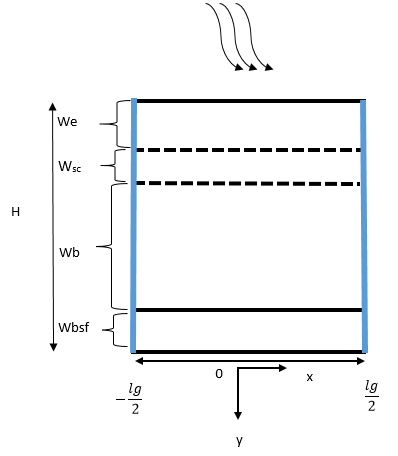
Figure 1 displays the assumed geometry of the poly-Si solar cell structure under illumination. It consists of an n+type emitter, a p type base and an p+ type layer which acts as a BSF. Their thicknesses are respectively We, Wb and Wbsf.
Figure 1. Solar cell geometry considered in the model
The model area consists of one grain and two grain boundaries extending vertically at the edges.
To simplify the model, the following considerations have been taken into account:
1. Low-level injection assumption
2. The study is limited to a front side illumination.
3. The electric field, carrier mobility, lifetime and diffusivity in p+ region are represented by an average value.
4. Doping and electric field dependent carrier mobility is assumed in BSF region.
5. The mobility in emitter and base layers depends on the doping according to the model presented by Dugas and Oualid [16].
6. Both SHR and Auger recombination are considered.
7. The thickness of the structure is the only factor influencing the generation rate.
8. The recombination velocities at grain boundaries are independent of generation rate.
The new model supposes that the solar cell has both a field free region and a thin region near to the back surface. This last region is characterized by an average constant field and a distance Wbsf. Depending on its direction, this field accelerates the photocarriers away or towards the back surface.
To explore the back surface field effect on electron distribution in high-low junction, we need to solve the continuity equations, which are as follows:
$\frac{{{\partial }^{2}}\Delta n(x,y)}{{{\partial }^{2}}x}+\frac{{{\partial }^{2}}\Delta n(x,y)}{{{\partial }^{2}}y}-\frac{1}{{{L}^{2}}}\Delta n\left( x,y \right)=-\frac{G(y)}{{{D}_{n}}}$ (1)
$\begin{align} & \frac{{{\partial }^{2}}\Delta {{n}_{bsf}}(x,y)}{{{\partial }^{2}}x}+\frac{{{\partial }^{2}}\Delta {{n}_{bsf}}(x,y)}{{{\partial }^{2}}y}+\frac{{{\mu }_{nbsf}}}{{{D}_{nbsf}}}E\frac{\partial \Delta {{n}_{bsf}}(x,y)}{\partial y} \\ & -\frac{1}{L_{bsf}^{2}}\Delta {{n}_{bsf}}(x,y)=-\frac{G(y)}{{{D}_{nbsf}}} \\ \end{align}$(2)
where, Dn(x, y), Dnbsf(x, y) are the excess minority carrier density, Dn, Dnbsf the diffusion constant, and L, Lbsf the diffusion length in p and p+ region respectively; µnbsf is the carrier mobility in BSF region.
E is the average constant field due to impurity gradient given by:
$E=\frac{1}{{{w}_{bsf}}}\int\limits_{{{w}_{e}}+{{w}_{sc}}+{{w}_{b}}}^{H}{\frac{kt}{q}}\frac{1}{N(y)}\frac{dN(y)}{dy}dy$ (3)
where, N(y) is the doping density in p+ region expressed as:
$N\left( y \right)={{N}_{a}}+{{N}_{bsf}}\exp \left( -{{\left( \frac{y-H}{\sigma } \right)}^{2}} \right)$ (4)
where, Na, Nbsf are respectively the base and BSF doping levels, whereas σ denotes the standard deviation [17].
G is the generation rate written as [13]:
$G\left( y \right)=\sum\limits_{i=1}^{3}{{{g}_{i}}{{e}^{-{{\alpha }_{i}}y}}}$ (5)
where, parameters gi and αi are generation rate and absorption coefficient in AM1.5 G illumination condition [18].
The solutions of (1) and (2) are expressed as [13]:
$\Delta n(x,y)=\sum\limits_{k}{{{X}_{k}}(y)}.\cos \left( {{c}_{k}}x \right)$ (6)
$\Delta {{n}_{bsf}}(x,y)=\sum\limits_{k}{{{Y}_{k}}(y).\cos ({{s}_{k}}x)}$ (7)
The carrier density is computed for k range from 1 to 10, which has been found to be sufficient to get a good convergence whatever the grain size and the recombination velocity as reported by Kolsi et al. [19], while the coefficients ck, sk are determined from the following boundary conditions. These boundary conditions are expressed in terms of the convenient balance of currents, by equating the minority carrier diffusion current and the grain boundary recombination current:
${{\left[ \frac{\partial \Delta n(x,y)}{\partial x} \right]}_{x=\pm \frac{\lg }{2}}}=\frac{\mp {{S}_{gb}}}{{{D}_{n}}}\Delta n(\pm \frac{\lg }{2},y)$ (8)
${{\left[ \frac{\partial \Delta {{n}_{nbsf}}(x,y)}{\partial x} \right]}_{x=\pm \frac{\lg }{2}}}=\frac{\mp {{S}_{GB}}}{{{D}_{nbsf}}}\Delta {{n}_{nbsf}}(\pm \frac{\lg }{2},y)$ (9)
here, Sgb and SGB represent the grain boundary recombination velocity in p and p+ regions respectively and lg the grain size.
Replacing Dn(x, y) and Dnbsf(x, y) by their expressions (6) and (7) respectively into the above two boundary conditions leads to the following transcendental equations (see Appendix):
${{c}_{k}}\tan \left( {{c}_{k}}\frac{\lg }{2} \right)=\frac{{{S}_{gb}}}{{{D}_{n}}}$ (10)
${{s}_{k}}\tan \left( {{s}_{k}}\frac{\lg }{2} \right)=\frac{{{S}_{GB}}}{{{D}_{nbsf}}}$ (11)
where, ck and sk are Eigen values of these transcendental equations are solved graphically.
Replacing the expressions of Dn(x, y) and Dnbsf(x, y) in the continuity Eqs. (1) and (2) respectively, we get after some simplifications the following differential equations:
$\frac{{{\partial }^{2}}{{X}_{k}}(y)}{\partial {{y}^{2}}}-\frac{1}{L_{k}^{2}}{{X}_{k}}(y)=-\frac{1}{{{D}_{k}}}G(y)$ (12)
$\begin{align} & \frac{{{\partial }^{2}}{{Y}_{k}}(y)}{\partial {{y}^{2}}}+\frac{{{\mu }_{nbsf}}}{{{D}_{nbsf}}}E\frac{\partial {{Y}_{k}}(y)}{\partial y}-\frac{1}{Lb_{k}^{2}}{{Y}_{k}}(y) \\ & =-\frac{1}{D{{b}_{k}}}G(y) \\ \end{align}$ (13)
where,
${{L}_{k}}=\frac{1}{\sqrt{c_{k}^{2}+\frac{1}{{{L}^{2}}}}}$ (14)
${{D}_{k}}=\frac{{{D}_{n}}(\sin ({{c}_{k}}\lg )+{{c}_{k}}\lg )}{4\sin ({{c}_{k}}\frac{\lg }{2})}$ (15)
$L{{b}_{k}}=\frac{1}{\sqrt{s_{k}^{2}+\frac{1}{L{{b}^{2}}}}}$ (16)
$D{{b}_{k}}=\frac{{{D}_{nbsf}}(\sin ({{s}_{k}}\lg )+{{s}_{k}}\lg )}{4\sin ({{s}_{k}}\frac{\lg }{2})}$ (17)
where, L and Lbsf are respectively the diffusion length in the base and BSF regions given by:
$L=\sqrt{{{D}_{n}}.{{\tau }_{n}}}$ (18)
${{L}_{bsf}}=\sqrt{{{D}_{nbsf}}.{{\tau }_{nbsf}}}$
The minority carrier mobility and lifetime as a function of doping N in the base area, can be represented by the following relations [19]:
${{\mu }_{n}}=232+\frac{1180}{1+{{\left( \frac{N}{{{8.10}^{16}}} \right)}^{0.9}}}$ (20)
${{\tau }_{n}}=\frac{1}{3.45.*{{0}^{-12}}N+0.95*{{10}^{-31}}{{N}^{2}}}$ (21)
In the BSF region, the same above expressions are used. Nevertheless, it is important to consider here the impact of the large values of the average longitudinal electric field on the electron mobility.
In this regard, we utilize the following relation [17]:
${{\mu }_{nbsf}}={{\mu }_{n}}\sqrt{\frac{1}{1+{{\left( \frac{{{\mu }_{n}}.E}{Vsat} \right)}^{2}}}}$ (22)
In this expression, μn is the carrier mobility at low electric field given by Eq. (20), and Vsat the saturation velocity equal to 107 cm.s-1.
It is important to mention that the carrier mobility is not altered for a given electric field of moderate strength. Nevertheless, it is decreased as a result of scattering caused by an increase in the longitudinal electric field.
The solutions Xk(y) and Yk(y) of Eqs. (12) and (13) respectively can be written in the form [13]:
${{X}_{k}}(y)={{A}_{k}}{{e}^{\frac{y}{{{L}_{k}}}}}+{{B}_{k}}{{e}^{-\frac{y}{{{L}_{k}}}}}-\sum\limits_{i=1}^{3}{\left( {{G}_{i}}{{e}^{-{{\alpha }_{i}}y}} \right)}$ (23)
${{Y}_{k}}(y)={{C}_{k}}{{e}^{\frac{{{M}_{k}}y}{L{{b}_{k}}}}}+{{F}_{k}}{{e}^{-\frac{{{N}_{k}}y}{L{{b}_{k}}}}}-\sum\limits_{i=1}^{3}{\left( {{R}_{i}}{{e}^{-{{\alpha }_{i}}y}} \right)}$ (24)
with:
${{G}_{i}}=\frac{L_{k}^{2}{{g}_{i}}}{(L_{k}^{2}{{\alpha }_{i}}^{2}-1){{D}_{k}}}$ (25)
${{R}_{i}}=\frac{Lb_{k}^{2}{{g}_{i}}}{D{{b}_{k}}(1+{{\alpha }_{i}}(\frac{{{\mu }_{nbsf}}}{{{D}_{nbsf}}}E-{{\alpha }_{i}})Lb_{k}^{2})}$ (26)
${{M}_{k}}=\frac{\frac{{{\mu }_{nbsf}}}{{{D}_{nbsf}}}E*L{{b}_{k}}+\sqrt{{{\left( \frac{{{\mu }_{nbsf}}}{{{D}_{nbsf}}}E \right)}^{2}}Lb_{k}^{2}+4}}{2L{{b}_{k}}}$ (27)
${{N}_{k}}=\frac{\frac{{{\mu }_{nbsf}}}{{{D}_{nbsf}}}E*L{{b}_{k}}-\sqrt{{{\left( \frac{{{\mu }_{nbsf}}}{{{D}_{nbsf}}}E \right)}^{2}}Lb_{k}^{2}+4}}{2L{{b}_{k}}}$ (28)
Constants Ak, Bk, Ck and Fk are determined using Maple software and by mean of the following boundary conditions:
${{X}_{k}}(y={{w}_{e}}+{{w}_{sc}})=0$ (29)
At pp+ interface, it can be stated that the current and the electron concentration are continuous [9].
So, we can write:
${{X}_{k}}(y={{w}_{e}}+{{w}_{sc}}+{{w}_{b}})={{Y}_{k}}(y={{w}_{e}}+{{w}_{sc}}+{{w}_{b}})$ (30)
$\begin{align} & {{D}_{n}}{{\left[ \frac{\partial {{X}_{k}}}{\partial y} \right]}_{y={{w}_{e}}+{{w}_{sc}}+{{w}_{b}}}}= \\ & {{\mu }_{nbsf}}E.{{Y}_{k}}({{W}_{e}}+{{W}_{sc}}+{{W}_{b}})+ \\ & {{D}_{nbsf}}{{\left[ \frac{\partial {{Y}_{k}}}{\partial y} \right]}_{y={{w}_{e}}+{{w}_{sc}}+{{w}_{b}}}} \\ \end{align}$ (31)
At y=H
${{D}_{nbsf}}{{\left[ \frac{\partial {{Y}_{k}}}{\partial y} \right]}_{y=H}}=-{{Y}_{k}}(Sb+{{\mu }_{nbsf}}E)$ (32)
The calculated photogenerated carrier density permits us to evaluate the solar cell’s output parameters.
3.1 Photocurrent density
In the base region of the solar cell, the photocurrent density is computed as follows [13]:
$Jp{{h}_{b}}=\frac{q{{D}_{n}}}{\lg }\int\limits_{-\frac{\lg }{2}}^{\frac{\lg }{2}}{{{\left[ \frac{\partial \Delta n(x,y)}{\partial y} \right]}_{y={{w}_{e}}+{{w}_{sc}}}}}dy$ (33)
where, q the electron charge.
In the BSF region, the generated photocurrent density can be written as:
$\begin{align} & Jp{{h}_{bsf}}=\frac{q{{D}_{nbsf}}}{\lg }\int\limits_{-\frac{\lg }{2}}^{\frac{\lg }{2}}{{{\left[ \frac{\partial \Delta {{n}_{bsf}}(x,y)}{\partial y} \right]}_{y={{w}_{e}}+{{w}_{sc}}+{{w}_{b}}}}}dx \\ & +\frac{q{{\mu }_{nbsf}}E}{\lg }\int\limits_{-\frac{\lg }{2}}^{\frac{\lg }{2}}{\Delta {{n}_{bsf}}{{(x,y)}_{y={{w}_{e}}+{{w}_{sc}}+{{w}_{b}}}}}dx \\\end{align}$ (34)
The Eq. (35) is used to calculate the photocurrent in the space charge layer [19]:
${{J}_{sc}}=\sum\limits_{i=1}^{3}{\frac{q.{{g}_{i}}}{{{\alpha }_{i}}}}.{{e}^{-{{\alpha }_{i}}{{w}_{e}}}}(1-{{e}^{-{{\alpha }_{i}}.{{w}_{sc}}}})$ (35)
Wsc is the space region thickness given by:
${{w}_{sc}}=\sqrt{\frac{2.\varepsilon }{q}\left( \frac{1}{{{N}_{a}}}+\frac{1}{{{N}_{d}}} \right)0.026\ln \left( \frac{{{N}_{a}}Nd}{{{n}_{i}}^{2}} \right)}$ (36)
Taking into account the homogenous doping level in the emitter region, the current density Jphe generated in this region at we can be expressed as follows using the same method as in the base region.
$Jp{{h}_{e}}=\frac{q{{D}_{p}}}{\lg }\int\limits_{-\frac{\lg }{2}}^{\frac{\lg }{2}}{\mathop{\left[ \frac{\partial \Delta p(x,y)}{\partial y} \right]}_{y={{w}_{e}}}}$ (37)
where, Dp(x, y) and Dp are respectively the excess minority carrier density and diffusion constant in n+ region.
The cell's total photocurrent density (Jph) is given by:
${{J}_{ph}}=Jp{{h}_{e}}+{{J}_{sc}}+Jp{{h}_{b}}+Jp{{h}_{bsf}}$ (38)
3.2 Open-circuit voltage
The open-circuit voltage can be linked to the total photocurrent density Jph and to the diode saturation current density Js by the following formula [9]:
${{V}_{oc}}=\frac{KT}{q}\ln (\frac{Jph}{Js}+1)$ (39)
To compute the saturation current, the calculation of the dark minority carrier concentration is performed under the assumption that the generation rate G is equal to zero [20].
3.3 Efficiency
Solar-cell conversion efficiency refers to the portion of energy in the form of sunlight that can be converted into electricity. It is given by Eq. (40) [21]:
$\eta =\frac{P\max }{Pinc}$ (40)
where, Pinc=0.1 W.cm-2 represents standard AM1.5 solar illumination conditions which models the spectral irradiance of sunlight on the earth's surface. This power density of 0.1 W/cm2 corresponds to 1 sun intensity, and Pmax is the maximum power point.
4.1 Minority carrier density
All results presented in this paper are computed using the numerical values indicated in Table 1.
Table 1. Physical parameters of an elementary cell used in the computation results
|
Parameters |
Value |
|
ɛ0 (F.cm-1) |
8.85 10-14 |
|
ɛr |
11.8 |
|
T (K) |
300 |
|
ni (cm-3) |
1.45 1010 |
|
Na (cm-3) |
1016 |
|
Nd (cm-3) |
1018 |
|
Nbsf (cm-3) |
1019 |
|
Sf (cm s-1) |
103 |
|
We (µm) |
0.6 |
|
Wsc (µm) |
0.3 |
|
Wb (µm) |
100 |
|
Wbsf (µm) |
0.5 |
|
Dn (cm2 s-1) |
32.62 |
|
Dp (cm2 s-1) |
7.52 |
|
Dnbsf (cm2 s-1) |
6.23 |
|
L (µm) |
307 |
|
Lbsf (µm) |
2.11 |
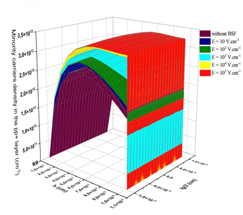
Figure 2. Effect of a positive field on minority carriers’ distribution with Sgb=103 cm.s-1, lg=20 µm, sb = 2000 cm.s-1, wbsf = 0.5 µm
Figure 2 displays the impact of the average positive electric field on the profile of excess minority carriers in the p and p+ areas, assuming Sb=2.103 cm.s-1, Sgb=103 cm.s-1 and wbsf=0.5 µm.
We can note that there is a depletion region at the rear surface. Indeed, the field is driving the carriers away from the surface into the field free region inducing higher their concentration in this region.
This effect is amplified by increasing the field magnitude.
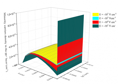
On the contrary, excess electrons are accumulated at the rear surface as shown in Figure 3, when the average electric field is negative.
Figure 3. Minority carriers’ distribution for a negative field with Sgb= 103 cm.s-1, lg=20 µm, wb=100 µm, Sb=2000 cm.s-1, Wbsf=0.5µm
In this case, the photo-generated carriers are driven towards the surface for recombining there making the concentration in the field free region lower than that in rear surface region. This effect is also enhanced for higher fields. As a result, there will be a decrease in the number of carriers collected, which will consequently reduce efficiency.
The acquired results are consistent with past investigations. In fact, the depletion and accumulation effects illustrated follow the expected behavior based on electric field direction and carrier transport physics in solar cells. Furthermore, the impact of field magnitudes on carrier density aligns well with predictions from several models of carrier transport.
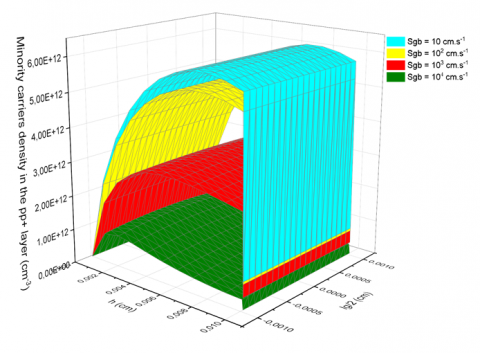
Figure 4 illustrates the minority carrier density with grain boundary recombination velocity Sgb as a parameter, assuming a moderate positive field of 103 V.cm-1. We note that by increasing the Sgb value, the excess carrier’s density within the field free region is decreased.
Figure 4. Minority carriers’ distribution for selected values of grain boundary recombination velocity for E=103 V.cm-1, lg=20 µm, wb= 100 µm, sb=2000 cm.s-1, wbsf=0.5 µm
As previously mentioned, the positive field is pushing the carriers away from the surface towards the base, increasing the recombination at grain boundaries which results in a decrease of carrier’s density there.
4.2 Performance parameters
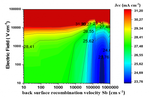
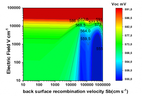
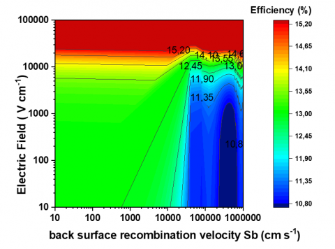
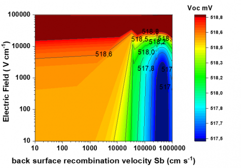
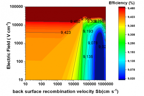
A simulation study was undertaken to analyze the influence of the average field E on polycrystalline-Si solar cell performances for the whole range of back surface recombination velocity. The results are illustrated in Figure 5.
One notes that all calculated photovoltaic parameters increase with increasing E, and that a moderate electric field around (5-8). 103 V.cm-1 negates any effect of surface recombination for value of Sb less or equal to 5.103 cm.s-1.
Also, towards higher back surface recombination velocities, the output parameters decrease indicating Sb limited performance.
Otherside, for higher fields, the photovoltaic parameters become much less sensitive to back surface recombination velocities, indicating bulk-lifetime-limited performance.
This last result emphasizes the importance of long bulk lifetimes. Therefore, improved bulk lifetimes augment overall performance of poly-Si solar cells by reducing grain boundary recombination velocity.
In practise, the effective recombination velocity Sgb at the grain boundary GB is related to the barrier height Eb, therefore to the electric field in GB space charge region, the density and the distribution of the interface states. So, the greater the value Sgb, the higher the electric field attracting more carriers to the grain boundary space charge area, prompting more recombinations.
This loss contributes to a marked decrease of solar cell performances.
(a) Current density Jcc
(b) Open circuit voltage Voc
(c) Efficiency h
Figure 5. Photovoltaic parameters as a function of electric field and back surface recombination velocity for wb=100 µm, Sgb=100 cm s-1, Wbsf=0.5 µm, lg=20 µm Jcc, (b) Voc, (c) Efficiency
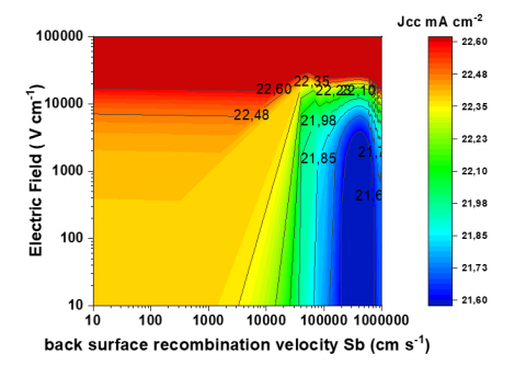
Consistent with this physical understanding, Figure 6 confirms clearly that high grain boundary velocity case (104 cm.s-1) actually produces smaller short circuit currents, open circuit voltages and consequently conversion efficiencies than the 100cm.s-1 recombination velocity case.
Using our model, the technical parameters characterizing the solar cell were determined for a conventional and BSF structures and compared to other works. The results are summarized in Table 2. Here, the effect of varying grain size on these parameters is investigated.
First, it is noted that grain size is critical because grain boundaries in polycrystalline silicon act as recombination sites for carriers. Smaller grain size means more boundaries and more recombination opportunity. In this case, the carrier collection is less important making poor the photovoltaic parameters. In the opposite, the overall content of defects is low in large grains and, as expected, all the cell parameters should improve.
Second, the quantitative improvements in performance with increasing grain size agree with expectations based on the reduced density of grain boundary trap states and recombination sites.
Additionally, the results suggest that conversion efficiency attained by BSF structure is more essential than a classical cell. The improvement is more than 7% depending on grain size lg.
For a grain size of 500 µm, the results reveal that adding a BSF layer improves the conversion efficiency from 14% for a classical n+p cell to 15.02 % for an n+pp+BSF cell under AM1.5 G conditions, an absolute increase of 1.02 % or a 7.2% relative increase.
At a smaller grain size of 20 μm, the improvement is less significant at 6.4% (9.9 % vs 9.3%).
(a) Current density Jcc
(b) Open circuit voltage Voc
(c) Efficiency h
Figure 6. Photovoltaic parameters as a function of electric field and back surface recombination velocity for (Sgb =104 cm.s-1, Wbsf=0.5 µm, lg =20 µm)
Table 2. Photovoltaic parameters for conventional solar cell and BSF solar cell assuming: wb=100 µm, Sgb=103 cm.s-1, sb=2000 cm.s-1, Sf=103 cm.s-1, Wbsf=0.5 µm, compared with other results
|
Photovoltaic Parameters |
Jcc (mA.cm-2) |
Voc (mV) |
Efficiency (%) |
FF (%) |
|
Conventional solar cell lg=20um |
23 |
545 |
9.3 |
74.19 |
|
BSF Solar cell lg=20 µm E=104 V.cm-1 |
24.1 |
550 |
9.9 |
74.68 |
|
Witout BSF Lg=100 µm |
27.8 |
570 |
13 |
82.03 |
|
BSF Solar cell lg=100 µm E=104 V.cm-1 |
29.7 |
617 |
13.9 |
75.85 |
|
Witout BSF Lg=500 µm |
28 |
590 |
14 |
84.74 |
|
Our results with BSF Solar cell lg=500 µm h=300 µm E=104 V.cm-1, |
29.8 |
620 |
15.02 |
81.29 |
|
Diallo et al. [13] lg=500 µm h=300 µm |
29.4 |
630 |
15.59 |
85.33 |
|
Narayanan et al. [14] |
36 |
623 |
17.8 |
79.36 |
|
Johnson and Winter [15] |
34.6 |
601 |
16.2 |
77.90 |
The photovoltaic parameters calculated in this section show good agreement with the values obtained by Diallo et al. [13]. For example, the short-circuit current density, the open-circuit voltage and the conversion efficiency match within 1.3%, 1.6% and 3.7% respectively for similar cell structures and material properties. This suggests the analytical model accurately captures the key physics governing carrier generation and collection.
However, the efficiency values differ from Narayanan et al. [14] by around 2.7% absolute for similar polycrystalline silicon cells. This is likely because some treatments have been developed in the study [14] to suppress the detrimental effect of grain boundaries. The qualitative trends are still consistent though.
Compared to the experimental results in Johnson and Winter [15], the modeled efficiencies are lower by around 1.1% absolute. This discrepancy primarily arises due to differences in material quality, particularly in bulk lifetimes.
The present model assumes lower lifetimes representative of as-grown polycrystalline silicon, while Johnson and Winter [15] employs processes to improve material quality.
However, overall the proposal model sufficiently captures the device physics to show excellent qualitative agreement.
Additionally, it is well known that the fill factor FF is related to the resistivity of the layer.
The higher the grain size lg, the fewer the defects will be, such that, less trapping states will occur in poly-Si films with massive crystalline grains. This leads to a greater free carrier concentration, that reduces the resistivity of the poly-Si film. This can explain the observed increase of FF with lg.
In this paper, a new model of back surface field poly-Si cells is proposed. It considers that a solar cell consists of three regions, a field free emitter and base, while the back region has a gaussian doping profile inducing consequently, an electric field there.
In this model, the built-in electric field is represented by an average value.
This assumption makes easy the solution of the 2D continuity equations to evaluate the distribution of excess minority carrier and the photovoltaic parameters of the device.
The results show a behavior that would be expected. For positive fields, the excess carriers show a depletion near the rear surface, whereas negative fields drive the photogenerated carriers towards the rear surface displaying an enhancement there.
Calculations of performance parameters reveal that positive and modest field E prevents any impact of surface recombination for values less or equal to 5.103 cm.s-1 while higher back surface recombination velocities indicate Sb limited performance.
For E higher than 104V.cm-1, the photovoltaic parameters become substantially less sensitive to back surface recombination velocities, indicating bulk-lifetime-limited performance.
Furthermore, the performance of the cell with the BSF structure is superior to that of the classical n+p structure. Depending on lg, the improvement in conversion efficiency can be as much as 7.2%. Our findings and those from studies published before [13-15] are fairly compatible.
Finally, we consider that the present model can be applied to any thin film silicon cell. The only assumption made is that of an average internal electric field to simplify the solution of the 2D continuity equations. We believe that it nevertheless doesn't alter the results.
However, additional factors could be considered in future studies such as expanding the model to 3D to better account for non-uniformities and edges effects in real solar cell geometries, exploring different non-uniform doping profiles beyond gaussian for the back surface field region, and validating the model predictions against experimental results across a wider range of fabrication processes and materials.
The work was funded by Algeria’s General Direction of Scientific Research and Technology (DGRSDT/MESRS). We gratefully acknowledge its financial support. We also thank the dedicated staff of Elaboration and Materials Characterization Laboratory for their insightful discussions and feedback, enhancing the quality of our work.
The continuity equations for excess minority charge in p and p+ regions are written as:
$\begin{align} & \frac{{{\partial }^{2}}\Delta n(x,y)}{{{\partial }^{2}}x}+\frac{{{\partial }^{2}}\Delta n(x,y)}{{{\partial }^{2}}y}-\frac{1}{{{L}^{2}}}\Delta n\left( x,y \right) \\ & =-\frac{G(y)}{{{D}_{n}}} \\ \end{align}$ (A.1)
$\begin{align} & \frac{{{\partial }^{2}}\Delta {{n}_{bsf}}(x,y)}{{{\partial }^{2}}x}+\frac{{{\partial }^{2}}\Delta {{n}_{bsf}}(x,y)}{{{\partial }^{2}}y}+ \\ & \frac{{{\mu }_{nbsf}}}{{{D}_{nbsf}}}E\frac{\partial \Delta {{n}_{bsf}}(x,y)}{\partial y} \\ & -\frac{1}{L_{bsf}^{2}}\Delta {{n}_{bsf}}(x,y)=-\frac{G(y)}{{{D}_{nbsf}}} \\ \end{align}$ (A.2)
The solutions of (A.1) and (A.2) are expressed as [13]:
$\Delta n(x,y)=\sum\limits_{k}{{{X}_{k}}(y).\cos ({{c}_{k}}x)}$ (A.3)
$\Delta {{n}_{bsf}}(x,y)=\sum\limits_{k}{{{Y}_{k}}(y).\cos ({{s}_{k}}x)}$ (A.4)
By setting the minority carrier diffusion current equal to the grain boundary recombination current, we can write:
${{\left[ \frac{\partial \Delta n(x,y)}{\partial x} \right]}_{x=\pm \frac{\lg }{2}}}=\frac{\mp {{S}_{gb}}}{{{D}_{n}}}\Delta n(\pm \frac{\lg }{2},y)$ (A.5)
${{\left[ \frac{\partial \Delta {{n}_{nbsf}}(x,y)}{\partial x} \right]}_{x=\pm \frac{\lg }{2}}}=\frac{\mp {{S}_{GB}}}{{{D}_{nbsf}}}\Delta {{n}_{nbsf}}(\pm \frac{\lg }{2},y)$ (A.6)
where, Sgb, SGB are respectively the grain boundary recombination velocity in p and p+ regions and lg the grain size.
Replacing Dn(x, y) and Dnbsf (x, y) by their expressions (A.3) and (A.4) respectively into the above two boundary conditions (expressions(A.5) and (A.6)) leads to the following equations:
${{\left[ \frac{\partial \Delta n(x,y)}{\partial x} \right]}_{x=\frac{\lg }{2}}}=-\frac{{{S}_{gb}}}{{{D}_{n}}}\Delta n(\frac{\lg }{2},y)$ (A.7)
This means:
$-{{X}_{k}}(y){{c}_{k}}\sin ({{c}_{k}}\frac{\lg }{2})=\frac{-{{S}_{gb}}}{{{D}_{n}}}{{X}_{k}}(y)\cos ({{c}_{k}}\frac{\lg }{2})$ (A.8)
Which results in:
${{c}_{k}}\tan \left( \frac{{{c}_{k}}\lg }{2} \right)=\frac{{{S}_{gb}}}{{{D}_{n}}}$ (A.9)
For x=-lg/2
${{\left[ \frac{\partial \Delta n(x,y)}{\partial x} \right]}_{x=-\frac{\lg }{2}}}=\frac{{{S}_{gb}}}{{{D}_{n}}}\Delta n(-\frac{\lg }{2},y)$ (A.10)
So,
${{X}_{k}}(y){{c}_{k}}\sin ({{c}_{k}}\frac{\lg }{2})=\frac{{{S}_{gb}}}{{{D}_{n}}}{{X}_{k}}(y)\cos ({{c}_{k}}\frac{\lg }{2})$ (A.11)
Resulting in:
${{c}_{k}}\tan \left( {{c}_{k}}\frac{\lg }{2} \right)=\frac{{{S}_{gb}}}{{{D}_{n}}}$ (A.12)
The same method gives the following expression in p+ region.
${{s}_{k}}\tan \left( {{s}_{k}}\frac{\lg }{2} \right)=\frac{{{S}_{GB}}}{{{D}_{nbsf}}}$ (A.13)
After that the coefficients ck, sk are determined graphically.
Replacing the expressions of Dn(x, y) and Dnbsf(x, y) in the continuity equations (A.1) and (A.2) respectively, we get the following differential equations:
$\begin{align} & \frac{{{\partial }^{2}}({{X}_{k}}(y).\cos ({{c}_{k}}x))}{{{\partial }^{2}}x}+\frac{{{\partial }^{2}}\left( {{X}_{k}}(y).\cos ({{c}_{k}}x) \right)}{{{\partial }^{2}}y} \\ & -\frac{1}{{{L}^{2}}}\left( {{X}_{k}}(y).\cos ({{c}_{k}}x) \right)=-\frac{G(y)}{{{D}_{n}}} \\ \end{align}$ (A.14)
Let’s multiply both sides of the Eq. (14) bycos(cnx).
Let’s leverage the orthogonality property of the function cos(cn.x), what means that:
$\begin{align} & \int\limits_{-\lg /2}^{\lg /2}{\cos ({{c}_{k}}x)}\cos ({{c}_{n}}x)\partial x= \\ & \left\{ _{\frac{\sin \left( {{c}_{k}}\lg \right)+{{c}_{k}}\lg }{2{{c}_{k}}}\mathop{{}}^{{}}(k=n)}^{0\mathop{{}}^{{}}k\ne n} \right. \\ \end{align}$ (A.15)
after simplification, we get:
$\frac{{{\partial }^{2}}{{X}_{k}}(y)}{\partial {{y}^{2}}}-\frac{1}{L_{k}^{2}}{{X}_{k}}(y)=-\frac{1}{{{D}_{k}}}G(y)$ (A.16)
And
$\begin{align} & \frac{{{\partial }^{2}}{{Y}_{k}}(y)}{\partial {{y}^{2}}}+\frac{{{\mu }_{nbsf}}}{{{D}_{nbsf}}}E\frac{\partial {{Y}_{k}}(y)}{\partial y}- \\ & \frac{1}{Lb_{k}^{2}}{{Y}_{k}}(y)=-\frac{1}{D{{b}_{k}}}G(y) \\ \end{align}$ (A.17)
With:
$\begin{align} & {{X}_{k}}(y)={{A}_{k}}{{e}^{\frac{y}{{{L}_{k}}}}}+ \\ & {{B}_{k}}{{e}^{-\frac{y}{{{L}_{k}}}}}-\sum\limits_{i=1}^{3}{\left( {{G}_{i}}{{e}^{-{{\alpha }_{i}}y}} \right)} \\ \end{align}$ (A.18)
$\begin{align} & {{Y}_{k}}(y)={{C}_{k}}{{e}^{\frac{{{M}_{k}}y}{L{{b}_{k}}}}}+ \\ & {{F}_{k}}{{e}^{-\frac{{{N}_{k}}y}{L{{b}_{k}}}}}-\sum\limits_{i=1}^{3}{\left( {{R}_{i}}{{e}^{-{{\alpha }_{i}}y}} \right)} \\ \end{align}$ (A.19)
replacing equations (A.18) and (A.19) in equations (A.3) and (A.4), we obtain:
$\Delta n(x, y)=\sum_k\left(\begin{array}{c}A_k e^\frac{y}{L_k}+B_k e^{-\frac{y}{L_k}}- \sum_{i=1}^3\left(G_i e^{-\alpha_i y}\right) \\\end{array}\right) .\cos\left(s_k x\right)$ (A.20)
$\begin{aligned} & \Delta n_{b s f}(x, y)= \sum_k\left(\begin{array}{c}Y_k(y)=C_k e^{\frac{M_k y}{L b_k}}+ F_k e^{-\frac{N_k y}{L b_k}}-\sum_{i=1}^3\left(R_i e^{-\alpha_i y}\right)\end{array}\right) \cdot \cos \left(s_k x\right)\end{aligned}$ (A.21)
Constants Ak, Bk, Ck and Fk are determined using Maple software and by mean of the following boundary conditions:
${{L}_{k}}=\frac{1}{\sqrt{c_{k}^{2}+\frac{1}{{{L}^{2}}}}}$ (A.22)
${{D}_{k}}=\frac{{{D}_{n}}(\sin ({{c}_{k}}\lg )+{{c}_{k}}\lg )}{4\sin ({{c}_{k}}\frac{\lg }{2})}$ (A.23)
$L{{b}_{k}}=\frac{1}{\sqrt{s_{k}^{2}+\frac{1}{L{{b}^{2}}}}}$ (A.24)
where, Lk, Lbk is the effective diffusion length.
With:
$D{{b}_{k}}=\frac{{{D}_{nbsf}}(\sin ({{s}_{k}}\lg )+{{s}_{k}}\lg )}{4\sin ({{s}_{k}}\frac{\lg }{2})}$ (A.25)
${{R}_{i}}=\frac{Lb_{k}^{2}{{g}_{i}}}{D{{b}_{k}}(1+{{\alpha }_{i}}(\frac{{{\mu }_{nbsf}}}{{{D}_{nbsf}}}E-{{\alpha }_{i}})Lb_{k}^{2})}$ (A.26)
${{M}_{k}}=\frac{\frac{{{\mu }_{nbsf}}}{{{D}_{nbsf}}}E*L{{b}_{k}}+\sqrt{{{\left( \frac{{{\mu }_{nbsf}}}{{{D}_{nbsf}}}E \right)}^{2}}Lb_{k}^{2}+4}}{2L{{b}_{k}}}$ (A.27)
${{N}_{k}}=\frac{\frac{{{\mu }_{nbsf}}}{{{D}_{nbsf}}}E*L{{b}_{k}}-\sqrt{{{\left( \frac{{{\mu }_{nbsf}}}{{{D}_{nbsf}}}E \right)}^{2}}Lb_{k}^{2}+4}}{2L{{b}_{k}}}$ (A.28)
${{G}_{i}}=\frac{L_{k}^{2}{{g}_{i}}}{(L_{k}^{2}{{\alpha }_{i}}^{2}-1){{D}_{k}}}$ (A.29)
${{R}_{i}}=\frac{Lb_{k}^{2}{{g}_{i}}}{D{{b}_{k}}(1+{{\alpha }_{i}}(\frac{{{\mu }_{nbsf}}}{{{D}_{nbsf}}}E-{{\alpha }_{i}})Lb_{k}^{2})}$ (A.30)
${{M}_{k}}=\frac{\frac{{{\mu }_{nbsf}}}{{{D}_{nbsf}}}E*L{{b}_{k}}+\sqrt{{{\left( \frac{{{\mu }_{nbsf}}}{{{D}_{nbsf}}}E \right)}^{2}}Lb_{k}^{2}+4}}{2L{{b}_{k}}}$ (A.31)
${{N}_{k}}=\frac{\frac{{{\mu }_{nbsf}}}{{{D}_{nbsf}}}E*L{{b}_{k}}-\sqrt{{{\left( \frac{{{\mu }_{nbsf}}}{{{D}_{nbsf}}}E \right)}^{2}}Lb_{k}^{2}+4}}{2L{{b}_{k}}}$ (A.32)
[1] Bechlaghem, S., Zebentout, B., Benamara, Z. (2018). The major influence of the conduction-band-offset on Zn(O, S)/CuIn0.7Ga0.3Se2 solar cells. Results in Physics, 10: 650-654. http://doi.org/10.1016/j.rinp.2018.07.006
[2] Dabbabi, S., Ben Nasr, T., Kamoun-Turki, N. (2017). Parameters optimization of CIGS solar cell using 2D physical modeling. Results in Physics, 7: 4020–4024. http://doi.org/10.1016/j.rinp.2017.06.057
[3] Mataré, H.F., Kostiner, E. (1971). Defect electronics in semiconductors. The Electrochemical Society, 119(8): 257. http://doi.org/10.1149/1.2404420
[4] Teodoreanu, A.M., Friedrich, F., Leihkauf, R., Boit, C., Leendertz, R., Korte, L. (2013). 2D modelling of polycrystalline silicon thin film solar cells. EPJ Photovoltaics, 4: 45104. http://doi.org/10.1051/epjpv/2013017
[5] Taretto, K.R. (2003). Modeling and characterization of polycrystalline silicon for solar cells and microelectronics. University of Stuttgart 05 Faculty of Computer Science, Electrical Engineering and Information Technology. http://doi.org/10.18419/opus-2513
[6] Distefano, T.H., Cuomo, J.J. (1977). Reduction of grain boundary recombination in polycrystalline silicon solar cells. Applied Physics Letters, 30: 351-353. https://doi.org/10.1063/1.89396.
[7] Sundaresan, R., Burk, D.E., Fossum, J.G. (1984). Potential improvement of polysilicon solar cells by grain boundary and intragrain diffusion of aluminum. Journal of Applied Physics, 55(4): 1162-1167. https://doi.org/10.1063/1.333210
[8] Karade, V.C., Jang, J.S., Kumbhar, D., Rao, M., Pawar, P.S., Kim, S., Kim, J.H. (2022), Combating open circuit voltage loss in sb2se3 solar cell with an application of Zns as a back surface field layer. Solar Energy, 233: 435-445. http://doi.org/10.1016/j.solener.2022.01.010
[9] Godlewski, M.P., Baraona, C.R., Brandhorst, H.W. (1990). Low-high junction theory applied to solar cells. Solar Cells, 29: 131-150. https://doi.org/10.1016/0379-6787(90)90022-W
[10] Fossum, J.G. (1977). Physical operation of back-surface-field silicon solar cells. IEEE Transactions on Electron Devices, 24(4): 322-325. http://doi.org/10.1109/T-ED.1977.18735
[11] Del Alamo, J., Van Meerbergen, J., d'Hoore, F., Nijs, J. (1981). High-low junctions for solar cell applications. Solid-State Electronics, 24(6): 533-538. http://doi.org/10.1016/0038-1101(81)90072-1
[12] Blouke, M.M., Delamere, A.W., Womack, G. (1991). Simplified model of the back surface of a charge-coupled device. In Charge-Coupled Devices and Solid State Optical Sensors II, pp. 142-155.
[13] Diallo, H.L., Seidou Maiga, A., Wereme, A., Sissoko G. (2008). New approach of both junction and back surface recombination velocities in a 3D modelling study of a polycrystalline silicon solar cell. The European Physical Journal-Applied Physics, 42(3): 203-211. http://doi.org/10.1051/epjap:2008085
[14] Narayanan, S., Wenham, S.R., Green, M.A. (1990). 17.8-percent efficiency polycrystalline silicon solar cells. IEEE Transactions on Electron Devices, 37(2): 382-384. http://doi.org/10.1109/16.46370
[15] Johnson, S.M., Winter, C. (1984). High efficiency large area polysilicon solar cells. In 17th IEEE Photovoltaic Specialists Conference, pp. 1121-1126.
[16] Dugas, Oualid, J. (1987), A model of the dependence of photovoltaic properties on effective diffusion length in polycrystalline silicon, Solar Cells, 20,167-176. http://doi.org/10.1016/0379-6787(87)90026-3
[17] Roldan, J.B., Gamiz, F., Lopez-Villanueva, J.A. (1997). A closed-loop evaluation and validation of a method for determining the dependence of the electron mobility on the longitudinal-electric field in MOSFETs. IEEE Transactions on Electron Devices, 44(9): 1447-1453. https://doi.org/10.1109/16.622600
[18] Furlan, J., Amon, S. (1985). Approximation of the carrier generation rate in illuminated silicon. Solid-State Electronics, 28(12): 1241-1243. http://doi.org/10.1016/0038-1101(85)90048-6
[19] Kolsi, S., Amar, M.B., Samet, H., Ouali, A. (2010). A new method of modelling a n+ pp + Polycrystalline solar cell under illumination. Echologic Vehicles. Renewable Energies.
[20] Godlewski, M.P., Baraona, C.R., Brandhorst Jr, H.W. (1973). The drift field model applied to the lithium-containing silicon solar cell. In Photovoltaic Specialists Conference (No. NASA-TM-X-71489), pp. 13-15.
[21] Leila, A., Afek, M., Ahmed, I., Halima, Z. (2021). Analysis and optimization of the performance of hydrogenated amorphous silicon solar cell. Journal of New Materials for Electrochemical Systems, 24(3): 151-158. http://doi.org/10.14447/jnmes.v24i3.a02