Abeer S. Alfayhan*![]() | Nahida B. Hasan
| Nahida B. Hasan
© 2024 The authors. This article is published by IIETA and is licensed under the CC BY 4.0 license (http://creativecommons.org/licenses/by/4.0/).
OPEN ACCESS
In this study, CZTS (Copper Zinc Tin Sulfide) thin films were fabricated using the pulse laser deposition (PLD) technique. Pellets formed under a pressure of 5 tons were ablated with a Nd:YAG laser at a pulse energy of 700 mJ. The resulting plasma plume was generated through a range of pulse counts—200, 250, 300, 350, and 400—at a consistent frequency of 6 Hz. The structural properties of the films were investigated via X-ray diffraction (XRD) and atomic force microscopy (AFM). XRD analysis revealed a polycrystalline tetragonal structure of the CZTS thin films, with an increase in peak quantity correlating to higher pulse counts. Concurrently, variations in grain size, strain, dislocation density, and lattice constants (a,c) manifested an irregular pattern as a function of pulse count. AFM assessments—comprising parameters such as root-mean-square (RMS) roughness, average diameter, and arithmetic mean height—indicated a peak in surface roughness at the maximum pulse quantity of 400. Optical properties were characterized using a UV-Visible Spectrophotometer (2700) across a spectrum ranging from 300 to 1100 nm. An increment in absorbance was noted with the rise in pulse number, whereas the direct bandgap exhibited a decrease from 3.6 to 2.8 eV. The films demonstrated exceptional potential for sensor applications, evidenced by transmittance levels exceeding 90%. Optical constants, including refractive index and extinction coefficient, were derived from the spectral data. The comprehensive analysis suggests that by manipulating the pulse count during PLD, not only can the structural properties of CZTS thin films be tailored, but their optical attributes can be optimized, paving the way for advanced applications in photonic sensors and other optoelectronic devices.
pulse laser, absorbance, transmittance, energy gap, grain size, roughness, square root rate
CZTS emerges as a compelling quaternary semiconductor, which is an amalgamation of I2-II-IV-VI4 group elements, encompassing sulfur (S), copper (Cu), zinc (Zn), and tin (Sn). The kesterite phase of CZTS, which is achieved by substituting the divalent Zn and tetravalent Sn for trivalent In/Ga elements, has been the focus of considerable research [1]. Since its discovery by Nakazawa et al. more than two decades ago [2], CZTS has been synthesized as a thin film through spray pyrolysis among other methods.
CZTS is recognized for its glycoprotein properties and is utilized in photovoltaic cells as a sorbent [3]. It presents a direct bandgap ranging from 1.4 to 1.5 eV, which is optimal for absorption in the visible spectrum, and it surpasses an absorption coefficient of 104 cm-1 [4]. The economic feasibility of CZTS is underscored when compared with prevalent light-absorbing compounds such as Cu(In,Ga)(S,Se)2 and CuInS2 [5]. Moreover, its environmental credentials are bolstered by the absence of noble and highly toxic elements, rendering the compound an environmentally benign alternative with excellent thermal stability [6].
The relevance of CZTS in sustainable energy applications has escalated due to the pressing demand for renewable energy resources. Its potential for large-scale deployment in thin-film solar cells hinges on the material's cost-effectiveness and lower ecological footprint. The tunable electronic properties of CZTS, stemming from its variable stoichiometry and crystal structure, have been extensively characterized, revealing a versatility conducive to various applications in optoelectronics and photonics.
In summary, the advent of CZTS as a thin-film material for solar cells marks a significant stride towards the development of renewable energy technologies. Its advantageous absorption characteristics, stability under operational conditions, and benign environmental impact affirm its status as a pivotal material in the quest for green and sustainable energy solutions.
We used the Cu2ZnSnS4 semiconductor as a pure (99.9%) powder-ready material with a pulsed laser deposition method. First, hydraulics were used to press the material. It was a Chinese-made hydraulic press with a press strength of (5 tones) that was used to make pellets of Cu2ZnSnS4 semiconductor powder. The CZTS compound pellets were about 5mm thick and 3cm in diameter. Nd- YAG laser with a wavelength of 1064 nm with pulse energy 700 mJ at a frequency of 6 Hz was used to make five samples with pulses number (200, 250, 300, 350, and 400). It slopes at an angle of about 45o. The crystal structure of compound films Cu2ZnSnS4 was determined using X-ray diffraction. The samples were analyzed using a Shimadzu XR-DIFRACTOMETER 6000 with a Cu target. Current: 30 mA, Voltage: 40 kV, Range (2σ): 20–80The parameters of the lattice dimensions (a, c), strain (ʔ), and dislocation density (δ) were computed utilizing a computer programme. The objective was to determine the topography of thin films of the CZTS compound that were prepared using varying numbers of pulses. A Strom-equipped Atomic Force Microscope (AFM) model 3100 was utilized to examine the topography of the thin films that were prepared. The absorbance and transmittance spectra of CZTS films were determined through optical measurements using a UV-Visible Spectrophotometer 2700. The optical constants, including the refractive index (n), absorption coefficient (α), and extinction coefficient (k), were computed after the optical energy gap (Eg) was measured.
(CZTS) thin films was prepared using a laser with a wavelength of 1064nm and a power of 700mJ with different number of pulses (200, 250, 300 and 400). It has a polycrystalline with tetragonal structure with planes (112) (206) (112) at angles (2ϴ = 28.53o, 40.76o and 41.96o) respectively.
Table 1. X-ray parameters for Cu2ZnSnS4 thin films prepared at different pulse numbers
|
Sample |
2θ (deg.) |
FWHM (deg.) |
Int. (c/s) |
d(hkl) Exp. (Å) |
G.S (nm) |
d(hkl) Std. (Å) |
(hkl) |
Lattice Constants (Å) |
Strain |
Dislocation Density |
Card No. |
|
CZTS-200 |
28.53 |
1.08 |
120 |
3.13 |
7.63 |
3.13 |
(112) |
a=5.434 c=10.856 tetragonal |
0.03 |
0.017 |
96-900-4751 |
|
40.76 |
1.42 |
60 |
2.21 |
5.95 |
2.23 |
(206) |
0.01 |
0.028 |
96-900-4751 |
||
|
41.96 |
0.41 |
70 |
2.15 |
20.91 |
2.15 |
(112) |
0.05 |
0.002 |
96-900-4751 |
||
|
CZTS-250 |
28.6 |
1.02 |
170 |
3.12 |
8.07 |
3.14 |
(112) |
a=5.434 c=10.856 tetragonal |
0.04 |
0.015 |
96-900-4751 |
|
33.6 |
1.04 |
119 |
2.67 |
8.02 |
2.63 |
(020) |
0.12 |
0.016 |
96-900-4751 |
||
|
46.6 |
2.08 |
90 |
1.95 |
4.15 |
1.93 |
(312) |
0.13 |
0.058 |
96-900-4751 |
||
|
56 |
2.20 |
80 |
1.64 |
4.09 |
1.64 |
(206) |
0.53 |
0.060 |
96-900-4751 |
||
|
59.8 |
1.76 |
85 |
1.55 |
5.20 |
1.53 |
(316) |
0.02 |
0.037 |
96-900-4751 |
||
|
CZTS-300 |
27.8 |
2.16 |
180 |
3.21 |
3.79 |
3.14 |
(112) |
a=5.434 c=10.856 tetragonal |
0.13 |
0.070 |
96-900-4751 |
|
32.2 |
0.99 |
140 |
2.78 |
8.35 |
2.73 |
(204) |
0.23 |
0.014 |
96-900-4751 |
||
|
45.4 |
1.08 |
100 |
2.00 |
8.01 |
2.01 |
(123) |
0.20 |
0.016 |
96-900-4751 |
||
|
56.6 |
1.08 |
90 |
1.62 |
8.36 |
1.63 |
(312) |
0.27 |
0.014 |
96-900-4751 |
||
|
62.2 |
1.96 |
92 |
1.49 |
4.74 |
1.40 |
(206) |
0.47 |
0.044 |
96-900-4751 |
||
|
76.6 |
2.06 |
89 |
1.24 |
4.92 |
1.24 |
(316) |
0.42 |
0.041 |
96-900-4751 |
||
|
CZTS-350 |
28.48 |
1.72 |
110 |
3.13 |
4.77 |
3.13 |
(020) |
a=5.434 c=10.856 tetragonal |
0.04 |
0.044 |
96-900-4751 |
|
32.96 |
1.03 |
90 |
2.72 |
8.05 |
2.72 |
(220) |
0.18 |
0.015 |
96-900-4751 |
||
|
38.84 |
1.37 |
60 |
2.32 |
6.15 |
2.31 |
(204) |
0.29 |
0.026 |
96-900-4751 |
||
|
39.97 |
1.58 |
70 |
2.25 |
5.34 |
2.25 |
(206) |
0.17 |
0.035 |
96-900-4751 |
||
|
CZTS-400 |
28.53 |
1.35 |
130 |
3.13 |
6.10 |
3.13 |
(112) |
a=5.434 c=10.856 tetragonal |
0.04 |
0.027 |
96-900-4751 |
|
32.94 |
1.07 |
110 |
2.72 |
7.77 |
2.72 |
(020) |
0.19 |
0.017 |
96-900-4751 |
||
|
45.503 |
1.26 |
80 |
1.99 |
6.86 |
2.01 |
(123) |
0.23 |
0.021 |
96-900-4751 |
||
|
56.5 |
0.83 |
75 |
1.63 |
10.88 |
1.63 |
(312) |
0.21 |
0.008 |
96-900-4751 |
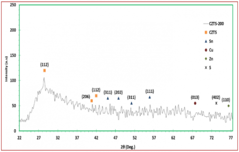
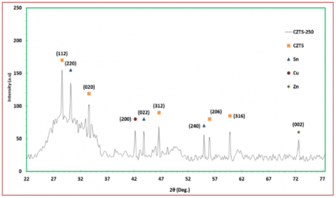
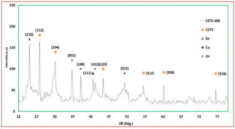
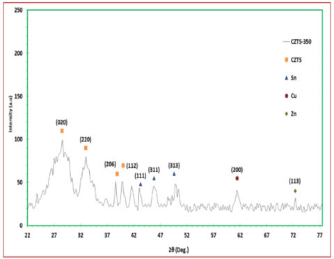
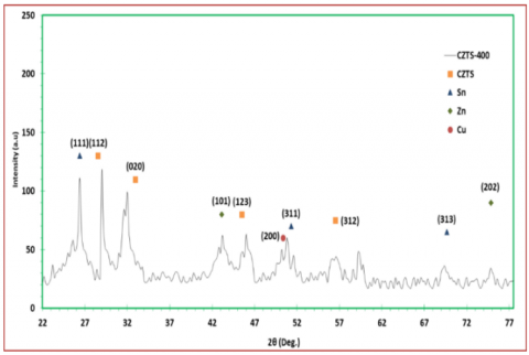
The preferred orientation at the angle (2ϴ = 28.53o) returns to the plane (112). Using the card number (96-900-4751) from the ICDD (International Center for Diffraction Data), diffraction was verified. When the number of pulses increased from 200 to 250 pulses, we notice that the dominant plane is (112). When the number of pulses increased the value of FWHM is drop, which mean the grain size had increased. It was also investigated how the number of pulses affected the grain size rate determined by Scherer’s equation. When the number of pulses increase, the kinetic energy of the atoms (CZTS) increases, which makes it easier for atoms in the crystalline lattice to be occupied as a result of the occupation of the maximum number of deposited atoms, the grain boundaries are decreased, resulting in a drop in the value of FWHM. We discovered that when the number of pulses grows, so does the stress and the particle size. As seen in Table 1, the density of dislocations decreases with some of pulses number rises, and reduces as grain size grows. Because of their inverse relationship, which results in an increase in grain size as seen in Figures 1-5, this agreement with literature [7].
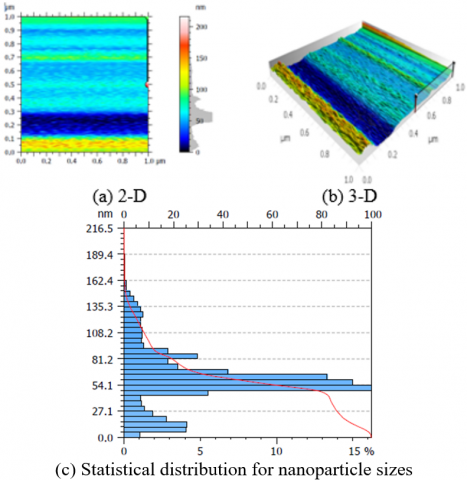
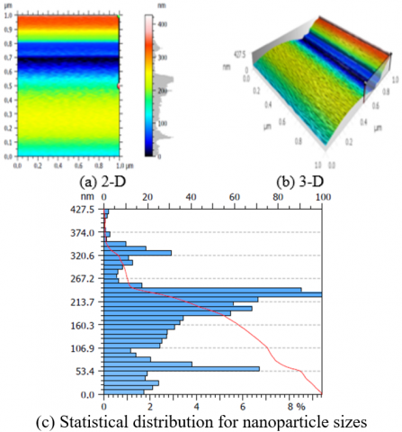
AFM is a resilient imaging technology that may be used to investigate the surface shape and characteristics of composite CZTS materials. AFM provides high-resolution imaging by scanning a sharp probe over the surface of a sample, detecting the interaction forces between the probe and the surface, and generating a topographic map of the surface [7]. In the context of composite CZTS materials also AFM can be used to investigate the microstructure and surface roughness of the composite film, as well as the distribution and arrangement of the CZTS particles within the composite [8]. Figures 6(a) and (b) shows the surface topography of the CZTS films created with a (700) mJ laser energy with 200 pulses of laser. The surface topography of the film revealed a number of nanostructures with average diameters (54.7) nm, the root mean square (RMS) equals (5.7) nm, and surface roughness about (3.8) nm. Arithmetic mean height Sa (19.69) nm and root-mean square height (27.46) nm. The findings of RMS values demonstrate that the nanoparticles are generated at this energy of laser, the surface's smoothness is shown by these values' tiny size, which supports the grains' small size. In fact, because of their small size, the surface is smooth. Figure 6(c) reflects the statistical distribution of average diameters percentages in the aforementioned deposition settings.
Figure 1. X-ray diffraction of CZTS films using 200 pulses
Figure 2. X-ray diffraction of CZTS films using 250 pulses
Figure 3. X-ray diffraction of CZTS films using 300 pulses
Figure 4. X-ray diffraction of CZTS films using 350 pulses
Figure 5. X-ray diffraction of CZTS films using 400 pulses
Figure 6. CZTS thin films at 200 pulses
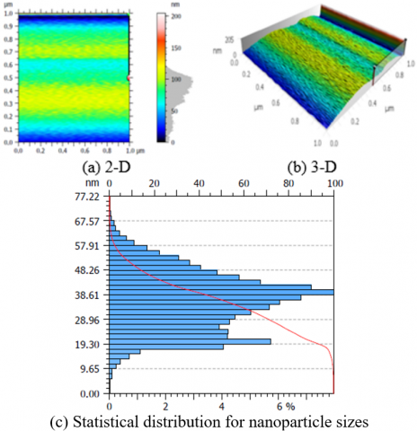
Figures 7(a) and (b) illustrate the surface topography of the CZTS films generated with a (700) mJ laser energy, 250 laser pulses, and a (1064) nm wavelength. Numerous nanostructures were discovered from the topography of the film surface, with average diameters (59.31) nm, mean square root (5.19) nm, and surface roughness is (3.10) nm. Through the RMS value, AFM pictures reveal a modest increase in the roughness of the measured surface. Figure 7(c) shows the statistical distribution of average diameters percentages under the aforementioned deposition conditions.
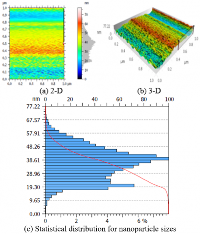
Figures 8(a) and (b) depict the topography of the CZTS films in two and three dimensions produced by a (700) mJ laser energy, 300 laser pulses, and a (1064) nm wavelength. The film surface topography revealed numerous nanostructures with average diameters (48.17) nm, mean square root (3.71) nm, surface roughness (2.65) nm, Arithmetic mean height (6.404) nm, and Root mean square height (17.311) nm. The images revealed a smoother surface than at low pulse counts, indicating reduced grain size and grain boundary development. This clearly reveals that the crystal structure of the film has shrunk, which improves the film's properties. Figure 8(c) depicts the statistical distribution of grain diameter percentages in the deposition.
Figure 7. CZTS thin films at 250 pulses
Figure 8. CZTS thin films at 300 pulses
Figures 9(a) and (b) depict the topography of the CZTS films in two and three dimensions produced by a (700) mJ laser energy, 350 laser pulses, and a (1064) nm wavelength. The topography of the film surface revealed numerous nanostructures with average diameters (51.24) nm, mean square root (RMS) about (7.81) nm, surface roughness is (3.69) nm, Root mean square height (66.86) nm, Arithmetic mean height (54.71) nm, and surface roughness is (3.69) nm. The statistical distribution of average diameters percentages under the aforementioned deposition circumstances is depicted in Figure 9(c).
Figure 9. CZTS thin films at 350 pulses
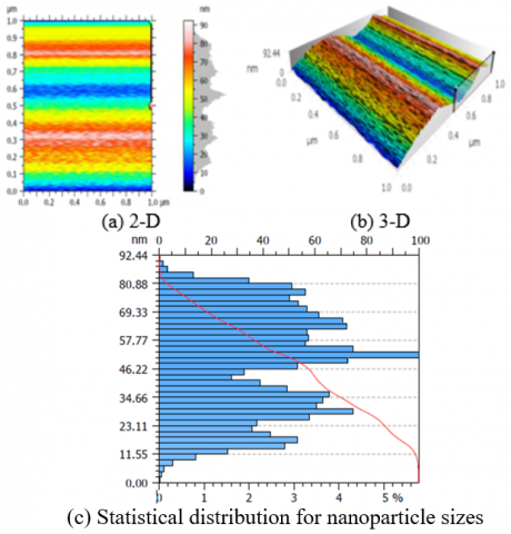
Figures 10(a) and (b) illustrate the topography of the CZTS films in two and three dimensions generated with a (700) mJ laser energy, 350 laser pulses, and a (1064) nm wavelength. The topography of the film surface revealed many nanostructures with average diameters (51.24) nm, mean square root (RMS) about (7.81) nm, surface roughness is (3.69) nm, Root mean square height (66.86) nm, Arithmetic mean height is (54.71) nm. Figure 10(c) depicts the statistical distribution of average diameters percentages under the aforementioned deposition conditions. The greatest crystalline granular tops on the surface are caused by an improvement in surface shape and average diameters, which can be seen from these photographs (Table 2). It has been discovered that all thin films exhibit an improvement in surface shape and average diameters as the number of pulses rises; this finding is consistent with (XRD) results [9].
Figure 10. CZTS thin films at 400 pulses
Table 2. AFM parameters for CZTS thin films at different pulses laser
|
Sample |
RMS (nm) |
Roughness (nm) |
Average Diameter (nm) |
Root Mean Square Height (Sq) (nm) |
Arithmetic Mean Height (Sa) (nm) |
|
CZTS200pules |
5.7 |
3.8 |
54.7 |
27.46 |
19.69 |
|
CZTS250pules |
5.19 |
3.10 |
59.31 |
29.28 |
18.32 |
|
CZTS300pules |
3.71 |
2.65 |
48.17 |
17.311 |
6.404 |
|
CZTS350pules |
7.81 |
3.96 |
51.24 |
66.86 |
54.71 |
|
CZTS400pules |
8.12 |
4.73 |
87.13 |
71.88 |
61.13 |
The optical properties of Cu2ZnSnS4 thin films deposited on glass substrate by pulse laser deposition technique (PLD) at laser energy (700) mJ and wavelength (1064) nm, as well as the number of laser pulses (200,250,300,350 and 400) were determined using the UV-VIS-IR transmittance spectrum in the range of (300-1100) nm. The optical properties of CZTS composites refer to how the material interacts with light, including its absorption, transmission, and reflection characteristics. These properties are determined by various factors such as the material's bandgap, refractive index, and scattering behavior.
5.1 Absorbance spectrum
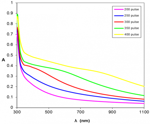
Figure 11 shows the relationship between the absorbance and wavelength of CZTS films produced using laser energy (700 mJ), wavelength (1064 nm), and number of laser pulses (200, 250, 300, 350, and 400 pulses).
Figure 11. Absorbance spectrum of CZTS films
The absorbance decreases with increasing wavelength for all prepared thin films [10]. When the number of laser pulses incident on a material increases, it can lead to an increase in the absorbance of CZTS. This phenomenon can be attributed to multiphoton absorption is the term used to describe a process in which an atom or molecule makes a single transition between two energy levels by absorbing the energy from more than a single photon [11]. In CZTS, the energy of incident photons is typically absorbed through the excitation of electrons from the valence band to the conduction band. However, in some cases, particularly with high-intensity laser pulses, multiple photons can simultaneously contribute to the excitation process. This is known as multiphoton absorption. With increasing laser pulse intensity, a higher number of photons interact simultaneously with the CZTS material, leading to a higher probability of multiphoton absorption. As a result, more electrons can be excited across the bandgap, increasing the overall absorbance of CZTS. It is important to note that the precise behavior of CZTS under high-intensity laser pulses can be influenced by various factors, such as the material's unique composition, defect density, and structural properties. The response will also depend on the specific wavelength and duration of the laser pulses used. Therefore, experimental characterization and modelling are necessary to obtain a detailed understanding of the absorption behavior of CZTS under different laser conditions [12].
5.2 Transmittance spectrum
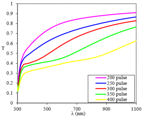
The connection between transmittance and wavelength of CZTS films made with laser energy (700) mJ wavelength (1064) nm and number of laser pulses (200, 250, 300, 350, 400) is depicted in Figure 12. Transmittance exhibited behavior that was diametrically opposed to absorption.
When the intensity of laser pulses incident on a CZTS material is increased, the transmittance of CZTS tends to decrease. This phenomenon can be attributed to two main effects: absorption and scattering Absorption: As the intensity of laser pulses increases, more photons are absorbed by the CZTS material. CZTS absorbs light through the excitation of electrons from the valence band to the conduction band. The absorbed photons are converted into thermal energy, which leads to an increase in the temperature of the material. As the temperature of CZTS rises due to absorption of the incident laser pulses, the material experiences thermal expansion. This expansion can contribute to structural changes, such as lattice distortion or the creation of defects, which in turn can affect the material's optical properties. These structural changes can cause increased absorption and decreased transmittance of additional laser pulses. When a high-intensity laser pulse interacts with CZTS, it can induce scattering of light within the material. Scattering occurs due to irregularities, impurities, or fluctuations in the composition and structure of CZTS. The scattering of light changes the direction of its propagation, preventing it from passing straight through the material and causing a decrease in transmittance. Furthermore, high-intensity laser pulses can also generate free carriers (electrons and holes) in CZTS via multiphoton absorption. The presence of free carriers can contribute to additional scattering due to their interaction with photons and lattice vibrations. Overall, the decrease in transmittance of CZTS with increasing laser pulse intensity is primarily a result of increased absorption and scattering of light within the material. However, the exact response of CZTS to high-intensity laser pulses can depend on various factors such as the material's composition, defect density, and structural properties. Experimental characterization and modeling are necessary to understand the specific behavior of CZTS under different laser conditions.
Figure 12. Transmittance spectrum of CZTS films
5.3 Absorption coefficient
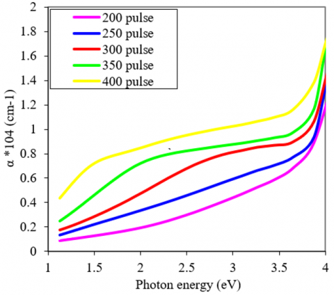
Figure 13 depicts the optical absorption coefficient of CZTS films made with laser energy (700 mJ), wavelength (1064 nm), and number of laser pulses (200, 250, 300, 350, and 400). It has been discovered that all of the thin films created had a high absorption coefficient (α > 104 cm-1), indicating an increase in the likelihood of direct transitions occurring.
Figure 13. Absorption coefficients for CZTS thin films
The figure shows that, when the intensity of laser pulses incident on CZTS is increased, the absorption coefficient of the material tends to increase. This can be attributed to a phenomenon known as saturation of the absorption process in CZTS. The absorption of light occurs when photons with energy greater than the bandgap excite electrons from the valence band to the conduction band. The absorption coefficient represents the ability of a material to absorb light and is defined as the fraction of incident light absorbed per unit distance traveled. At low laser pulse intensities, the absorption coefficient of CZTS is relatively low, as only a small fraction of incident photons has enough energy to excite electrons across the bandgap. However, as the intensity of laser pulses increases, more photons interact with the CZTS material simultaneously. With higher intensity, there is an increased probability of multiphoton absorption, where multiple photons contribute to the excitation process. This multiphoton absorption phenomenon allows the absorption of light with energies slightly below the bandgap, effectively extending the absorption range of CZTS. As the intensity continues to increase, there is a point where the absorption process reaches saturation. At this point, the CZTS material becomes saturated with electrons in the conduction band, and further increases in laser pulse intensity do not lead to a proportional increase in the absorption of light. The saturation effect limits the ability of CZTS to absorb additional photons, resulting in an increase in the absorption coefficient. The absorbed photons can then be converted into thermal energy, which can lead to structural changes and affect the material's optical properties, as discussed in the previous response. Because of this, the absorption coefficient of CZTS tends to go up as the laser pulse intensity goes up. This is because of the effects of multiphoton absorption and the process becoming saturated. The specific parameters of the incident laser pulse, as well as the material's particular composition, defect density, and structural characteristics, all have an impact on these effects.
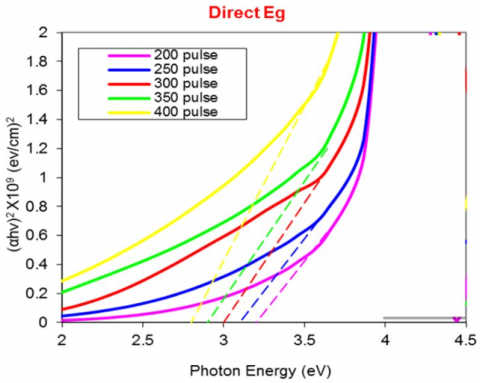
5.4 Optical energy gap
Absorption coefficients for CZTS thin films as a function of wavelength for various laser energies (700 mJ), wavelengths (1064 nm), and laser pulse counts (200, 250, 300, 350 and 400). Typical CZTS film absorption coefficients as a function of wavelength for various laser energy (700 mJ), wavelengths (1064 nm), and laser pulse counts (200, 250, 300, 350 and 400). We noted a rise in the number of laser pulses as the energy gap narrowed, as a consequence of the irritation of secondary levels inside the energy gap, and as a result, the width of the energy gap narrowed and the most grins were deposited on the substrate's surface. The optical energy gap values for CZTS films are shown in Table 3, we notice the energy gap value reduces as the number of laser pulses increases [13].
Figure 14. The optical energy gap for the allowed direct transition for CZTS films
Table 3. The optical energy gap values for CZTS thin films at laser energy (700) mJ, wavelength (1064) nm, and number of laser pulses (200, 250, 300, 350 and 400)
|
Sample |
Eg (eV) |
|
CZTS200pules |
3.2 |
|
CZTS250pules |
3.1 |
|
CZTS300pules |
3 |
|
CZTS350pules |
2.9 |
|
CZTS400pules |
2.8 |
5.5 Extinction coefficient
The value of the extinction coefficient is determined by the interactions between the electromagnetic wave and the medium, and is proportional to the exponential decay of the wave as it passes through the medium. The correlation between the extinction coefficient and the wavelength of deposited CZTS films is illustrated in Figure 14. Across all manufactured samples, the extinction coefficient (k) tends to increase as the number of pulses increases. Evidently, the k value for CZTS films, in general, the behavior of k is comparable to the behavior of. The damping coefficient is a parameter that characterizes the energy dissipation or decay of an oscillating system. When the number of laser pulses incident on CZTS is increased, it can lead to an increase in the damping coefficient. This increase in the damping coefficient can be attributed to increased electron-phonon interactions. When laser pulses interact with CZTS, they can generate free electrons and holes in the material. These free carriers can interact with the lattice vibrations (phonons) present in CZTS through electron-phonon scattering. With an increasing number of laser pulses, the population of free carriers also increases. Consequently, the interaction between the free carriers and phonons becomes more prominent. This increased electron-phonon scattering leads to higher energy dissipation and decay of the optical response, resulting in a higher damping coefficient. Thermal effects, when laser pulses are incident on CZTS, the material may absorb them, causing localized heating. This increase in temperature can induce thermal expansion, resulting in structural changes within the material. These structural changes can lead to variations in the optical properties, including an increase in the damping coefficient. The increased absorption of laser pulses with a higher number of pulses can contribute to a more significant temperature rise and subsequent thermal effects, leading to an increased damping coefficient.
(1) The pulsed laser deposition method has proven to be effective in creating thin films at nanoscale ranges and pressures (10–5 mbar). We made Cu2ZnSnS4 compound films by using different numbers of particles, a constant laser energy, and other laser parameters. X-ray diffraction analysis showed that these films are polycrystalline tetragonal, which is what happens when the number of particles increases during the ablation process of the target CZTS. The strain, dislocation density, and lattice constants (a, c) all decrease as grain size rises.
(2) Morphological studies using atomic force microscope (AFM) pictures revealed that the mixed materials contain nano-scale grains and that the size of the grains grew with increasing the number of pulses.
(3) The optical investigation revealed that the films were highly absorbed with a direct, allowed kind of transition.
(4) The increase in the pulse lasers decreases the value of energy gaps which causes the increase in absorption coefficient and extinction coefficient due to exist donor levels increases the probability of absorbing photons with long wavelengths, which reduces the energy gap.
(5) The optical analysis showed that the films had a direct and allowed transition.
(6) The number of laser pulses effects on structural and optical properties of films which play an effect roll for preparing photodetector, solar cell and gas sensor.
Suggestions for future work
(1) Studying the effect of thermal annealing, substrate temperature, and thickness on the optoelectronic properties of CZTS heterojunction.
(2) Fabrication and characterization of CZTS/Si solar cells by chemical spray pyrolysis technique.
(3) Studying the effect of different substrates (ITO, GaAs, and Ge) on the properties of Cu2ZnSnS4 thin films.
[1] Chen, S., Gong, X.G., Walsh, A., Wei, S. H. (2009). Crystal and electronic band structure of Cu2ZnSnX4 (X= S and Se) photovoltaic absorbers: First-principles insights. Applied Physics Letters, 94(4): 041903. https://doi.org/10.1063/1.3074499
[2] Khalaf, A.J., Hasan, N.B. (2020). Investigation optical properties of cuznsnsthin films prepared by pulse laser deposition. Journal of Critical Reviews, 7(1): 522-526. http://doi.org/10.31838/jcr.07.01.103
[3] Chen, S., Gong, X.G., Walsh, A., Wei, S.H. (2010). Defect physics of the kesterite thin-film solar cell absorber Cu2ZnSnS4. Applied Physics Letters, 96(2): 021902. https://doi.org/10.1063/1.3275796
[4] Sze, S.M., Li, Y., Ng, K.K. (2021). Physics of Semiconductor Devices. John Wiley & Sons.
[5] Nakazawa, K.I. (1988). Electrical and optical properties of stannite-type quaternary semiconductor thin films. Japanese Journal of Applied Physics, 27(11R): 2094. https://doi.org/10.1143/JJAP.27.2094.
[6] Nagoya, A., Asahi, R., Wahl, R., Kresse, G. (2010). Defect formation and phase stability of Cu2ZnSnS4 photovoltaic material. Physical Review B, 81(11): 113202. https://doi.org/10.1103/PhysRevB.81.113202
[7] Kumar, Y.K., Raja, V.S. (2017). Investigations on the growth of Cu2ZnSnS4 thin films for solar cell absorber layer. Surfaces and Interfaces, 9: 233-237. https://doi.org/10.1016/j.surfin.2017.10.003
[8] Patel, S.L., Purohit, A., Chander, S., Kannan, M.D., Dhaka, M.S. (2018). Towards post-NH4Cl treatment on CdSe thin films for solar cell applications. Vacuum, 153: 43-47. https://doi.org/10.1016/j.vacuum.2018.03.038
[9] Tanaka, T., Nagatomo, T., Kawasaki, D., et al. (2005). Preparation of Cu2ZnSnS4 thin films by hybrid sputtering. Journal of Physics and Chemistry of Solids, 66(11): 1978-1981. https://doi.org/10.1016/j.jpcs.2005.09.037
[10] Peksu, E., Karaagac, H. (2019). A third generation solar cell based on wet-chemically etched Si nanowires and sol-gel derived Cu2ZnSnS4 thin films. Journal of Alloys and Compounds, 774: 1117-1122. https://doi.org/10.1016/j.jallcom.2018.10.012
[11] He, G.S., Tan, L.S., Zheng, Q., Prasad, P.N. (2008). Multiphoton absorbing materials: Molecular designs, characterizations, and applications. Chemical Reviews, 108(4): 1245-1330. https://doi.org/10.1021/cr050054x
[12] Houimi, A., Gezgin, S.Y., Mercimek, B., Kılıç, H.Ş. (2021). Numerical analysis of CZTS/n-Si solar cells using SCAPS-1D. A comparative study between experimental and calculated outputs. Optical Materials, 121: 111544. https://doi.org/10.1016/j.optmat.2021.111544
[13] Qiu, L., Xu, J., Cai, W., Xie, Z., Yang, Y. (2019). Fabrication of Cu2ZnSnS4 thin films by microwave assisted sol-gel method. Superlattices and Microstructures, 126: 83-88. https://doi.org/10.1016/j.spmi.2018.12.020