Omar Raad Attallah*![]() | J. F. Mohammad
| J. F. Mohammad![]()
© 2023 IIETA. This article is published by IIETA and is licensed under the CC BY 4.0 license (http://creativecommons.org/licenses/by/4.0/).
OPEN ACCESS
In this study, thin films of Cadmium Sulfide (CdS) were prepared on glass substrates at a temperature of 350℃ using the Chemical Spray Pyrolysis (CSP) technique.Cadmium chloride and thiourea were used as sulfur sources.The structural properties and surface morphology of the CdS thin films were characterized using X-ray diffraction (XRD) and atomic force microscopy (AFM). The XRD analysis revealed that all the prepared films exhibited a polycrystalline hexagonal structure, with multiple peaks and angles, and a preferred orientation along the (002) direction. The XRD results also indicated that an increase in the solution concentration led to a significant increase in intensity and a slight increase in the crystallite size of the CdS film.AFM analysis was performed to investigate the surface structure of the films. The results showed that as the molarity increased, the surface roughness, grain size, and root mean square (RMS) roughness increased. This can be attributed to the increased molar concentration, which resulted in a slight increase in droplet size. However, despite these surface roughness variations, the prepared films can still be used as windows in Optical applications and Gas Sensors. The optical properties, including transmittance, absorbance, and band gap energy, were determined by measuring the absorbance spectrum using a UV-Visible Spectrophotometer within the wavelength range of 300 nm to 1100 nm. The CdS films exhibited transmittance values ranging from approximately 76% to 35%. The band gap energy of the films ranged between 1.85 eV and 2.38 eV. It was observed that as the concentration increased, the transmittance decreased and the absorbance spectrum increased, indicating a narrower band gap energy. Our findings suggest that controlling the molarity in the Chemical Spray Pyrolysis method can influence the structural and optical properties of CdS thin films, potentially impacting their use. in Optical applications and Gas Sensors. So, the optimal molar concentration for the preparation of the CdS film was found to be 0.03 M for both cadmium chloride and thiourea. This is achieved through the results of textural and optical properties.
CdS thin films, Chemical Spray Pyrolysis (CSP), Group II-VI, CdS structural characteristics
Cadmium Sulfide (CdS) compound is a semiconductor material classified as a chalcogenide due to its sulfur (S) content. It belongs to Group II-VI of the periodic table. (CdS) exists in the form of yellow-colored crystals and is widely used in various applications, including solar cells [1]. practical applications, optical sensors, and other fields [2]. (CdS) is considered an n-type semiconductor, but it can be converted into p-type thin films by doping with impurities such as copper (Cu) or indium (In) atoms [3]. (CdS) has a direct band gap energy of approximately 2.4 eV at a temperature of 300 K [4]. CdS thin films are polycrystalline and exhibit a crystalline structure of either zincblende or hexagonal type, as shown in Figure 1. These films possess suitable electrical properties for solar cell applications [5]. Numerous experiments have shown that CdS is an ideal compound when used as a window layer in thin-film solar cells, such as those based on CuInGaSe or CdTe [6]. Its cut-off wavelength occurs at approximately 520 nm in the visible spectrum, indicating that the film absorbs light at wavelengths shorter than 520 nm, while longer wavelengths are transmitted through the film [7]. (CdS) thin films can be prepared using various methods, including thermal evaporation under vacuum [8]. Chemical Spray Pyrolysis [9, 10]. chemical bath deposition, and others [11, 12]. In our study, we relied on the Chemical Spray Pyrolysis technique for preparing CdS films due to its low cost, ease of use, ability to produce large-area films with good adhesion and uniformity. Additionally, this method allows for the mixing of two or more materials with different melting points [13]. Many researchers have studied and prepared CdS membranes using various preparation methods and other parameters. We will mention some of them in upcoming paragraph.
The two studies were conducted by Pandya and Raval [14]. By preparing CdS films on glass bases at a temperature of 200℃ using deposited by chemical technique with different molar concentration. Structural tests showed a multiple crystal structure with a cubic shape and the preferred dominant direction (111) with a crystal size ranging between (1.5 - 2) nm with increasing concentration. Molar also showed that optical tests have a direct energy gap between (2.4-2.7) eV and decrease with increasing concentration. Researchers also studied it by studying and preparing CdS films on glass substrates at various temperatures using a thermochemical decomposition method. The synthetic results (XRD) showed that the films have a polycrystalline structure and are hexagonal in shape, with the dominant (002) direction, regardless of about the substrate temperature. As for visual tests, they confirmed that the membranes prepared at different temperatures have a direct gap between (2.44 - 2.58) eV. The best membrane obtained was at a temperature of 300℃ [15].
The purpose of the study is to obtain the best CdS film for use as a window layer in optical and sensing applications in future projects. This is done by changing the molarity of the cadmium chloride and thiourea solutions while keeping the other experimental parameters constant, such as temperature, spraying rate, spraying pause time, and the height of the spraying device.
(a) Zincblende (b) Hexagonal
Figure 1. Crystal structure of CdS [5]
2.1 Glass substrate preparation
Glass slides of standard quality with a Chinese origin (Glass Slide Microscopic REF 217102) were utilized in this study. The slides were approximately cut into square pieces with dimensions of 2.5cm×2.5cm×1mm. These glass pieces were employed for the purpose of depositing thin films on them. Prior to deposition, the slides underwent the following cleaning procedures:
2.2 Preparation of spray solutions
Spray solutions with varying concentrations are prepared by dissolving cadmium chloride salts with thiourea supplied by Chemical Ltd, Poole, England, with a purity of 99.6%, in distilled water of specific purity as listed in Table 1. Each solution is prepared according to the following equation [16].
$W_t=M_{W t} \times M_t \times \frac{V}{1000}$ (1)
where:
$\mathrm{W}_{\mathrm{t}}$ : Weight required to be dissolved ( $\mathrm{g}$ ).
$\mathrm{M}_{\mathrm{t}}:$ Molar Concentration (M).
$\mathrm{M}_{\mathrm{Wt}}$ : Molecular Weight $(\mathrm{g} / \mathrm{mol})$.
V: Distilled water Volume (ml).
Table 1. Percentage of Salts used in preparation of (CdS) thin films membrane per molar concentration
|
The Molar Concentration (M) |
Net Weight )CH4N2S) (g) |
Net Weight (CdCl2.H2O) (g) |
Water Used for Dissolving Salt (ml) |
|
0.03 |
0.23 |
0.604 |
100 |
|
0.05 |
0.38 |
1.0066 |
100 |
|
0.07 |
0.53 |
1.41 |
100 |
After preparing the solutions, then put it on the magnetic stirrer for 25 minutes to ensure the homogeneity of the solution. equal volumes of cadmium chloride and thiourea solutions with a molar concentration of 0.03 were taken to prepare a (CdS) membrane. A quantity of 60 ml of the solution was sprayed onto glass substrates placed on an electric heater at a temperature of 350℃. This is because at this temperature good films were obtained in terms of crystallization and crystal growth. Nozzle height (30 + 2cm), with a duration of time (25 s), spray rate (5s), stop time (20s), and air pressure rate (3 bar).
3.1 X-ray diffraction
Figure 2 illustrates the X-ray diffraction (XRD) results of the (CdS) film at molarities of 0.03, 0.05, and 0.07 M. It can be observed that there are diffraction peaks corresponding to crystallographic planes, indicating a polycrystalline structure. The observed diffraction peaks correspond to crystal planes (100), (002), (101), (110), and (112) with diffraction angles of 24.7°, 26.5°, 28.14°, 44.3°, and 51.7°, respectively.
The dominant preferred orientation is along the (002) plane, indicating a hexagonal crystal structure. These results are consistent with the International Card JCPDS:77-2306. It was also found that increasing the concentration of the solution led to a significant increase in intensity and a slight increase in the crystallite size of the prepared (CdS) film.
Figure 2. XRD spectrographs for CdS thin film at molarities of (0.03, 0.05, 0.07) M
The best homogeneity was achieved at a concentration of 0.03 M. Furthermore, increasing the concentration to 0.07 M resulted in the appearance of low peaks corresponding to crystal planes (102), (103), (203), (114), and (105) at angles of 36.9°, 47.811°, 66.793°, 72.586° and, 75.615° respectively.
The reason for the clarity of the diffraction peaks with increasing molar concentration is due to the increase in the proportion of the sulfur ion $\left(\mathrm{S}^{-2}\right)$ combining with the cadmium ion $\left(\mathrm{Cd}^{+2}\right)$ in the formation of a compound $(\mathrm{CdS})$. The reason may be attributed to the transformation of the crystal structure from its hexagonal form to a cubic form, and this is consistent with the study of researchers [17].
Table 2 presents the crystallographic planes, diffraction angles, and crystalline size calculated using the Debye-Scherrer equation [18], for molarities M (0.03, 0.05, 0.07).
$\mathrm{D}=\frac{\mathrm{k} \lambda}{\beta \cos \theta}$ (2)
where:
D: Crystal size.
$\beta$ : Full Width Half Maximum (FWHM) in (rad).
$\mathrm{K}$ : Scherer's constant (0.94).
$\lambda$ : X-ray wavelength $\left(\mathrm{A}^{\circ}\right)$.
$\theta$ : Angle of Diffraction (Bragg's Angle).
Table 2. Results of XRD for CdS thin film at molarities of (0.03, 0.05, 0.07) M
|
Sample |
Molarity (M) |
(hkl) Hexag |
$2 \theta$ deg |
$\theta$ deg |
d nm |
FWHM rad |
$\boldsymbol{\beta}$ deg |
D nm |
$\mathbf{D}_{\text {av }} \mathbf{n m}$ |
|
CdS |
0.03 |
(100) (002) (101) |
24.2 25.8 27.6 |
12.1 12.9 13.8 |
0.37 0.35 0.32 |
1.144 0.886 1.074 |
0.086 0.015 0.019 |
7 10 8 |
8.3 |
|
CdS |
0.05 |
(100) (002) (101) |
24.3 26.0 27.6 |
12.2 13 13.8 |
0.37 0.32 0.32 |
0.721 0.829 0.696 |
0.013 0.014 0.012 |
12 10 12 |
11.3 |
|
CdS |
0.07 |
(100) (002) (101) |
24.9 26.4 28.2 |
12.4 13.2 14.1 |
0.36 0.34 0.32 |
0.683 0.619 0.358 |
0.012 0.011 0.006 |
13 14 25 |
17.3 |
Table 3. Structural parameters for CdS thin film at molarities of (0.03, 0.05, 0.07) M
|
Sample |
Molarity (M) |
t nm |
D nm |
$\boldsymbol{\beta}$ deg |
$\theta$ deg |
($\mathcal{E}$) |
$\mathbf{N}_0$ $\mathrm{nm}^{-2}$ |
$\mathbf{N}_{\mathbf{L}}$ |
$\delta$ $\mathbf{n m}^{-2}$ |
|
CdS |
0.03 |
400 |
7 10 8 |
0.085 0.015 0.019 |
12.1 12.9 13.8 |
0.021 0.004 0.005 |
1.2 0.4 0.8 |
57.1 40 50 |
0.02 0.01 0.015 |
|
CdS |
0.05 |
400 |
12 10 12 |
0.013 0.014 0.012 |
12.2 13 13.8 |
0.003 0.004 0.003 |
0.23 0.4 0.23 |
33.3 40 33.3 |
0.007 0.01 0.007 |
|
CdS |
0.07 |
400 |
13 14 25 |
0.012 0.011 0.006 |
12.4 13.2 14.1 |
0.003 0.0026 0.0015 |
0.18 0.145 0.098 |
30.8 28.6 16 |
0.006 0.005 0.002 |
Table 4. AFM data for CdS at molarities of (0.03, 0.05, 0.07) M
|
Sample |
Molarity (M) |
Ave Diameter )nm) |
RMS Roughness (nm) |
Ave Roughness )nm) |
|
CdS |
0.03 |
55.65 |
10.46 |
7.771 |
|
CdS |
0.05 |
92.64 |
34.02 |
28.07 |
|
CdS |
0.07 |
170.8 |
48.64 |
41.21 |
Table 3 illustrates the structural parameters calculated from the following equations:
$\delta=\frac{1}{D^2}$ (3)
$\delta$ : Dislocation density in $\left(\mathrm{mm}^{-2}\right)$.
$\mathrm{N}_{\mathrm{L}}=\frac{\mathrm{t}}{\mathrm{D}}$ (4)
where:
t: Film thickness (mm).
$\mathrm{N}_{\mathrm{o}}=\frac{\mathrm{t}}{\mathrm{D}^3}$ (5)
$\varepsilon=\frac{\beta \cos \theta}{4}$ (6)
where:
$\beta$: Full Width Half Maximum (FWHM).
$\theta$: Angle of Diffraction (Bragg’s Angle).
3.2 Atomic Force Microscope (AFM)
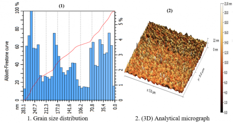
Figure 3 Illustrates three-dimensional (3D) atomic force micrographs and the grain size distribution of the $(\mathrm{CdS})$ film prepared at a temperature of $350^{\circ} \mathrm{C}$ using the Chemical Spray Pyrolysis (CSP) technique with different molarities of 0.03 , $0.05,0.07 \mathrm{M}$. It is evident that as the molarity increases, the surface roughness, grain size, and root mean square (RMS) value also increase. This can be attributed to the higher molar concentration, which slightly increases the droplet size. However, despite this, the prepared films can be used as windows in optical applications and gas sensors due to their high uniformity and smooth surface, which reduces reflectivity and enhances transmittance. The best film was obtained at a molarity of $0.03 \mathrm{M}$ This study is consistent with the researchers [22]. Table 4 presents the detailed AFM examination results for the ($\mathrm{CdS}$) film as mentioned above.
Figure 3a. Results of AFM for CdS film at Molarit of (0.03) M
Figure 3b. Results of AFM for CdS film at Molarit of (0.05) M
Figure 3c. Results of AFM for CdS film at Molarit of (0.07) M
3.3 Optical characteristics
The optical properties of the prepared (CdS) films were studied using a UV-Vis spectrophotometer to measure the transmittance and absorbance spectra as a function of wavelength within the range of 300-1100 nm. From these spectra, various optical properties such as the absorption coefficient and energy gap can be calculated.
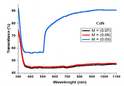
Figure $4 \mathrm{a}$ shows the transmittance spectrum of (CdS). The relationship between transmittance (T) as a function of wavelength $(\lambda)$ was plotted. The transmittance was around $76 \%$ at a wavelength of $520 \mathrm{~nm}$ in the visible spectrum. With an increase in molar concentration, the transmittance gradually decreases to approximately $35 \%$ at the same wavelength due to the increase in film thickness.
Figure $4 \mathrm{b}$ illustrates the relationship between absorbance (A) as a function of wavelength $(\lambda)$. The absorbance was around $25 \%$ at a wavelength of $520 \mathrm{~nm}$. With an increase in molar concentration, the absorbance gradually increases to approximately $36 \%$ due to the higher molar concentration.
Figure $4 \mathrm{c}$ presents the values of energy gaps $\left(\mathrm{E}_{\mathrm{g}}\right)$ for different concentrations 0.03, 0.05, 0.07 M. By using Tauc plot relation Eq. (7) [23].
$\alpha h v=B_o\left(h v-E_g\right)^{\frac{1}{2}}$ (7)
where:
$\alpha$: The absorption constant.
$h$: Plank's constant.
$\mathrm{B}_{\mathrm{o}}$: Constant.
$v$: The frequency of photon.
$E_g$: Enrge gap.
Figure 4a. Transmittance spectra for (CdS) film at molarities of (0.03, 0.05, 0.07) M
Figure 4b. Absorbance spectra for (CdS) film at molarities of (0.03, 0.05, 0.07) M
The results indicate that the films have energy gaps ranging from 1.853 eV to 2.38 eV, and an increase in molar concentration leads to a decrease in the energy gap due to the increase in solution concentration, which in turn increases the film thickness. Therefore, it is preferable to use the prepared (CdS) film with a concentration of 0.03 M as a window layer in in optical applications and gas sensors. This study is consistent with the researchers [24].
Figure 4c. Energy gap for (CdS) film at molarities of (0.03, 0.05, 0.07) M
From the current study of (CdS) films prepared using the Chemical Spray Pyrolysis method (CSP) on glass substrates at a temperature of 350℃ and at different molar concentrations.it was observed that the concentrations 0.03, 0.05, 0.07 M of both cadmium chloride and thiourea were taken in equal molar ratios to prepare (CdS).
The X-ray diffraction (XRD) results revealed that the films are polycrystalline with a hexagonal phase and possess crystalline planes (100), (002), (101), (110), (112), corresponding to diffraction angles of 24.7°, 26.5°, 28.14°, 44.3°, and 51.7°, respectively. The predominant preferred orientation was found at (002). Various structural characteristic parameters were calculated for each molar concentration. As for the atomic force microscopy (AFM) results, it was observed that with an increase in molar concentration, the surface roughness and grain size rate (RMS) also increased. This can be attributed to the slight increase in droplet size due to the higher molar concentration.
Regarding the optical properties, the transmittance, absorbance spectra, and energy gap showed that an increase in concentration leads to a decrease in transmittance and energy gap and an increase in absorbance spectrum.
Based on these examinations, it was concluded that the best-prepared (CdS) film in terms of structural and optical results is achieved at a molar concentration of (0.03 M). This film can be used as a window layer in solar cells due to its high homogeneity and smooth surface, which leads to reduced reflectivity, increased transmittance, and energy gap.
Our findings provide crucial insights into the optimization of CdS thin films as window layers in Solar Cells or in Optical applications and Gas Sensors, highlighting the promise of a 0.03 M concentration for achieving high performance.
[1] Baron, A.S., Mohammed, K.A., Abood, M.M. (2021). The role of Ag layer in the optical properties of CdS thin film. Chalcogenide Letters, 18(10): 585-588. https://doi:10.15251/CL.2022.193.183
[2] Fateh Mulla, A., Al-Dhafiri, A.M., Al-Ayashi, W.M., Al-Shammari, A.S. (2009). Synthesis and characterisation of chlorine doped cadmium sulphide (CdS: Cl) nanoparticles on flexible substrates. International Journal of Nanoparticles, 2(1-6): 476-482. https://doi:10.1504/IJNP.2009.028783
[3] Linsi, S., Kavitha, B., Dhanam, M., Maheswari, B. (2010). Analysis of Cu: CdS thin films of three different copper compositions. World Applied Sciences Journal, 10(2): 207-213
[4] Adachi, S. (2009). Properties of Semiconductor Alloys: Group-IV, III-V and II-VI Semiconductors. John Wiley & Sons, USA.
[5] Abbas, J.M., Hamad, K.I., Mustafa, F.I. (2018). Design and manufacture of solar cell from ITO/ZnO/CdS/CdTe by thermal vaporization technique and studying the physical properties. Journal of University of Anbar for Pure Science, 12(1): 98-105. https://doi.org/10.37652/juaps.2022.171609
[6] Chun, S., Jung, Y., Kim, J., Kim, D. (2011). The analysis of CdS thin film at the processes of manufacturing CdS/CdTe solar cells. Journal of Crystal Growth, 326(1): 152-156. https://doi.org/10.1016/j.jcrysgro.2011.01.086
[7] Johnson, P.K. (2003). The effect of trapping defects on CIGS solar-cell performance. Colorado State University, USA.
[8] Rahman, M.F., Hossain, J., Kuddus, A., Tabassum, S., Rubel, M.H., Shirai, H., Ismail, A.B.M. (2020). A novel synthesis and characterization of transparent CdS thin films for CdTe/CdS solar cells. Applied Physics A, 126: 1-11. https:/doi.org/10.1007/s00339-020-3331-0
[9] Mohammed, I.M., Gubari, G.M., Sonawane, M.E., Kasar, R.R., Patil, S.A., Mishra, M.K., Sharma, R. (2021). Influence of pH on the physical properties of CdS thin film and its photosensor application. Applied Physics A, 127: 1-10. https://doi.org/10.1007/s00339-021-04743-y
[10] Thiagarajan, R., Anusuya, M., Beevi, M.M. (2009). Mechanical characterization of spray pyrolytic cadmium sulphide thin films by indentation technique. Journal of American Science, 5: 51-56.
[11] Waldiya, M., Narasimman, R., Bhagat, D., Vankhade, D., Mukhopadhyay, I. (2019). Nanoparticulate CdS 2D array by chemical bath deposition: Characterization and optoelectronic study. Materials Chemistry and Physics, 226: 26-33. https://doi.org/10.1016/j.matchemphys.2019.01.017
[12] Garza-Hernández, R., Carrillo-Castillo, A., Martínez-Landeros, V.H., Martínez-Puente, M.A., Martínez-Guerra, E., Aguirre-Tostado, F.S. (2019). In-situ X-ray photoelectron spectroscopy analysis of the initial growth of CdS thin films by chemical bath deposition. Thin Solid Films, 682: 142-146. https://doi.org/10.1016/j.tsf.2019.04.003
[13] Schneller, T., Waser, R., Kosec, M., Payne, D. (2013). Chemical Solution Deposition of Functional Oxide Thin Films. Vienna: Springer Vienna.
[14] Pandya, S., Raval, K. (2017). Investigation of structural, morphological and optical properties of cadmium sulphide (CdS) thin films at different Cd/S concentration deposited by chemical technique. Journal of Materials Science: Materials in Electronics, 28(23): 18031-18039. https://doi.org/10.1007/s10854-017-7746-0
[15] Yadav, A.A., Barote, M.A., Masumdar, E.U. (2010). Studies on nanocrystalline cadmium sulphide (CdS) thin films deposited by spray pyrolysis. Solid state sciences, 12(7): 1173-1177. https://doi.org/10.1016/j.solidstatesciences.2010.04.001
[16] Igbinovia, E.O., Ilenikhena, P.A. (2010). Improved chemical deposition and thermal emittance of tin (iv) oxide (SnO2) thin films for photothermal conversion of solar energy and possible applications. International Journal of Physical Sciences, 5: 1770-1775.
[17] Mahdi, M.A., Hassan, Z., Ng, S.S., Hassan, J.J., Bakhori, S.M. (2012). Structural and optical properties of nanocrystalline CdS thin films prepared using microwave-assisted chemical bath deposition. Thin Solid Films, 520(9): 3477-3484. https:/doi.org/10.1016/j.tsf.2011.12.059
[18] Ashok, A., Regmi, G., Romero-Núñez, A., Solis-López, M., Velumani, S., Castaneda, H. (2020). Comparative studies of CdS thin films by chemical bath deposition techniques as a buffer layer for solar cell applications. Journal of Materials Science: Materials in Electronics, 31: 7499-7518. https://doi.org/10.1007/s10854-020-03024-3
[19] Kumar, A., Pednekar, D., Mukherjee, S., Choubey, R.K. (2020). Effect of deposition time and complexing agents on hierarchical nanoflake-structured CdS thin films. Journal of Materials Science: Materials in Electronics, 31: 17055-17066. https://doi.org/10.1007/s10854-020-04263-0
[20] Sze, S.M., Ng, K.K. (1981). Physics of Semiconductor Devices. John Wiley & Sons. New York, 68: 778.
[21] Mallick, P., Sahoo, C.S. (2013). Effect of CuO addition on the structural and optical properties of NiO nanoparticles. Nanoscience and Nanotechnology, 3(3): 52-55. https://doi:10.5923/j.nn.20130303.04
[22] Al-Fouadi, A.H.A., Hussain, D.H., Rahim, H.A. (2017). Surface topography study of CdS thin film nanostructure synthesized by CBD. Optik, 131: 932-940. https://doi.org/10.1016/j.ijleo.2016.11.175
[23] Verma, M., Dwivedi, P.K., Das, B. (2015). Structure–property correlation of pure and Sn-doped ZnO nanocrystalline materials prepared by co-precipitation. Journal of Experimental Nanoscience, 10(6): 438-448. https://doi.org/10.1080/17458080.2013.840936
[24] Moreno-Regino, V.D., Castañeda-de-la-Hoya, F.M., Torres-Castanedo, C.G., Márquez-Marín, J., Castanedo-Pérez, R., Torres-Delgado, G., Zelaya-Ángel, O. (2019). Structural, optical, electrical and morphological properties of CdS films deposited by CBD varying the complexing agent concentration. Results in Physics, 13: 102238. https://doi.org/10.1016/j.rinp.2019.102238