Vibrational Properties and Raman Peak Shift Relationships in Si1−xGex Epilayers Grown on Annealed Double Porous Silicon

Soraya Gouder*![]() | Ramdane Mahamdi
| Ramdane Mahamdi![]() | Dhouadi Guiza
| Dhouadi Guiza![]() | Isabelle Berbezier
| Isabelle Berbezier![]()
© 2023 IIETA. This article is published by IIETA and is licensed under the CC BY 4.0 license (http://creativecommons.org/licenses/by/4.0/).
OPEN ACCESS
Previous investigations into SiGe alloys using Raman spectroscopy have generated significant uncertainties regarding the relationships between shifts in Raman peak frequencies and stress. Furthermore, these studies did not establish precise correlations when examining alloys on porous substrates. These substrates have emerged as promising candidates in the highly competitive field of adaptable substrates for epitaxial growth of heterogeneous systems (such as III-V, SiGe, etc.) on Silicon (Si). Among these porous materials, double porous silicon (DPSi) has recently garnered attention, featuring a low porosity upper layer atop a buried high porosity layer. However, during a heat treatment, the upper low-porosity layer transforms into a quasi-monocrystalline Si layer, making it suitable for high-quality epitaxial growth. In this work, we present the first investigation of the vibrational properties of the Si1-xGex membranes grown on top of annealed DPSi, using Raman spectroscopy. We systematically propose new relationships linking the Raman peak shift to Ge concentration and strain, using a set of experimental equations derived from the peak positions of the Si-Si, Si-Ge, and Ge-Ge modes.
annealed double porous silicon, Raman spectroscopy, Si1-xGex epilayer, strain
Silicon (Si) is the cornerstone of the semiconductor industry due to its exceptional electrical properties, which enable the creation of transistors and microchips that power modern electronics. Its abundance, manufacturability, and reliability have made silicon the preferred material for decades. However, integrating optoelectronic devices into Si-based technology presents challenges because Si is not inherently suited for light emission and detection. The inherent disadvantage of this material is its indirect band gap which can be surmount by the introduction of SiGe heterostructure, especially that SiGe is relatively easy to integrate into silicon technology.
One of the major challenges in engineered SiGe-based devices has always been reducing the strain related with lattice parameter mismatch (4.2%) between pure materials, especially beyond a critical thickness [1-3] by avoiding development of misfit dislocations. Therefore, a suitable solution consists on the growth of a strain-relaxed SiGe buffer layer above a virtual Si (or Ge) substrate [4-7].
Recent advancements necessitate both downsizing dimensions and enhancing device performance, which in turn requires controlling stress in structures and understanding its origin. One promising approach that has emerged is the use of compliant substrates, particularly Porous Silicon (PSi), which is known for its flexibility [8, 9]. The soft and flexible nature of PSi allows it to effectively accommodate the stress shift introduced by the SiGe heteroepitaxial films, mainly due to its high pore density. Its compatibility with silicon-based microelectronics and its cost-effectiveness has opened up new possibilities for the integration of heterogeneous supra-axial systems (such as III-V or SiGe) on Si substrates [9, 10].
Recently, double porous Si (DPSi) has emerged as a prominent candidate in the competitive quest for compliant substrates, particularly for epitaxial growth in heterogeneous systems [11, 12]. This DPSi consists of an ultrathin, atomically flat layer on top, where the pores are stopped out, and a thick, highly porous layer beneath. Nevertheless, when attempting low-temperature epitaxy of SiGe and Ge on this DPSi layer, it resulted in the formation of rough epitaxial layers containing extended defects [13, 14].
However, thermal treatment of the DPSi layer undergoes significant morphological changes, converting small pores into larger ones and simultaneously generating tensile strain, as already reported in our previous study [9]. The morphological changes that DPSi undergoes are crucial in semiconductor fabrication processes, such as epitaxial layer transfer [15-19], making it an excellent alternative and a promising candidate for fabricating electronic devices and solar cells [20-22].
In this paper, we present the first systematic experimental study of the vibrational properties of a high quality monocrystalline SiGe layer grown on DPSi annealed at high temperature, using Raman spectroscopy. Our primary focus was to analyze the continuous variation trend of Ge content (x) and strain, with the aim of quantitatively determining the distribution of Ge content (x) and strain. The properties of SiGe are significantly influenced by its composition and stress. Stress impacts the energy band structure and lattice vibration, while composition affects the lattice constant and electron mobility [23-25]. To enable broader applications of SiGe on annealed DPSi, it becomes crucial to study the distribution of strain resulting from stress and composition. Raman spectroscopy serves as a valuable tool to characterize these factors, typically recording the peaks of Si-Si, Si-Ge, and Ge-Ge modes of SiGe. Since composition and strain can cause shifts in the Raman peaks, analyzing the Raman spectra allows for the calculation of their values. Consequently, equations describing the variation of Raman spectra with Ge content and strain in SiGe alloys have been derived through Raman spectroscopy.
The growth experiments were performed by Molecular Beam Epitaxy (MBE) in a Riber system. DPSi structures are obtained from a (001)-oriented B-doped Si wafer dipped in hydrofluoric acid (HF 25%) using electrochemical etching. The current density was varied between 10 mA.cm-2 and 80 mA.cm-2 leading to porosities between 20% and 30% [11]. DPSi layers are first annealed under hydrogen atmosphere at high temperature T (1100°C) for 60 seconds then introduced into the growth chamber. The annealing process permits us to obtain stable porous layer with improved structural and optical properties. The heat treatment triggers a structural transformation, converting small pores into larger ones with an average diameter of approximately 300 nm. This reconfiguration of the porous layer leads to its consolidation, creating an ideal seed layer for subsequent epitaxial growth. This layer serves as a vacancy sink, thus enabling the growth of Si or SiGe films with a minimized defect density, as previously outlined [9, 26]. To prepare the samples, the same cleaning procedure as previously reported in our earlier work was employed [9]. After that, they were immediately introduced into the ultrahigh vacuum chamber, where samples are outgassed at 400°C for 15min, avoiding the contamination of their surface. An ultrathin Si buffer layer is grown above SiGe layers by MBE in ultrahigh vacuum in order to avoid contaminants which could unintentionally affect surface. SiGe layers are deposited at 500°C.
The structure obtained is illustrated schematically in Figure 1, with particular focus on the dimensions of the different epitaxial layers.
Figure 1. Schematic representation of the SiGe structure deposited on annealed DPSi
The Raman measurements were carried using a Bruker spectrophotometer (SENTERIA), for excitation we use a beam of 488 nm line from argon laser at 10 mW output power.
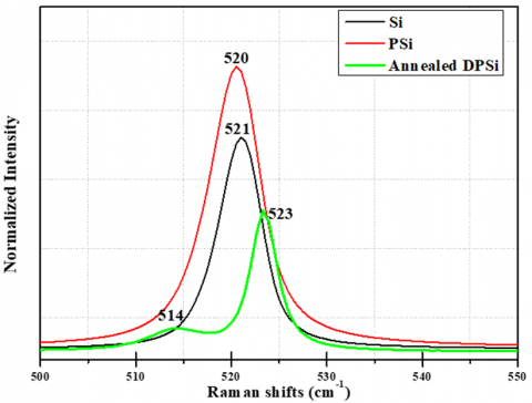
Figure 2 presents the Raman spectrum of annealed DPSi, along with a comparison to the Raman spectra of the as-etched PSi and a monocrystalline Si wafer. In the case of the monocrystal Si wafer, the Raman spectrum peak is observed at 521 cm−1, slightly higher than the peak for the as-etched PSi located at 520 cm−1. This shift in peak position is attributed to a tensile stress in the porous film caused by lattice expansion during anode etching. The phonon confinement mode, considering the effects of mechanical stresses, can explain this phenomenon. However, the Raman peak of DPSi shifts to a higher wave number at 523 cm−1. This shift aligns with the relaxation of lattice expansion relaxation and the restructuring of porous morphology due to annealing [27], this change is linked to an increase in pore diameter, which was previously demonstrated in our earlier research [9].
Figure 2. Raman spectrum of annealed DPSi, as-etched PSi and the monocrystal Si wafer
The presence of an additional Raman peak observed at 514 cm-1 indicates the existence of a tensely strained layer in the thin PSi layer free of pores. This tensile strain observed in DPSi results from high-temperature annealing, causing the lattice structure to swell. This expansion is induced by the removal of hydrogen during thermal annealing, leading to a significant reduction in the lattice parameter [28].
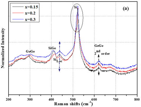
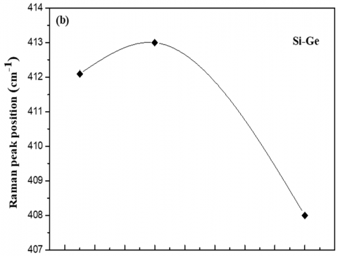
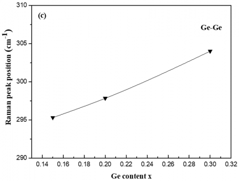
Figure 3 shows the Raman spectra of different samples, they include three distinct peaks whose positions and consequently the energies are related on the x (Ge content) and the strain [29]. These peaks correspond to the optical phonons resulting from the motion of adjacent Si-Ge, Ge-Ge, and Si-Si pairs, as demonstrated in the previous study [29]. Furthermore, the positions of all three peaks shift relative to each other depending on the value of x.
The vibrational frequencies obtained for several epilayers are presented in Table 1. A previously observed shoulder, denoted as SiLoc and located near the Si-Ge peak at approximately 438 cm-1, has been documented in prior research [30]. This shoulder is attributed to the movement of Ge atoms within specific local environments near Si atoms, as it closely aligns with the 438 cm-1 position.
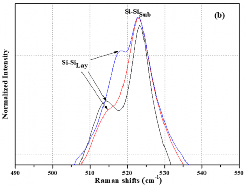
Figure 3. (a) Raman spectra of Si1-xGex grown on top of annealed DPSi, the circled area presents expanded views of the Si peaks (b)
It is noteworthy that the Raman Ge-Ge peak exhibits frequency shifts in relation to the Ge content. Specifically, it shifts to lower frequencies (or upper frequencies for x=0.3) compared to the Ge-Ge mode in bulk Ge, which typically occurs at 300 cm-1. This shift is attributed to a combination of composition and strain influences.
Additionally, the intensity of the Si-Ge modes is observed to peak above 408 cm-1. This contrasts with the growth of SiGe on a PSi substrate, where the corresponding mode was observed at lower frequencies (<400 cm-1), as reported in the previous study [31].
Table 1. Peak positions of different Raman modes of Si1-xGex grown on annealed DPSi
|
Sample Content (x) |
Si-Si (layer) (cm-1) |
Si-Ge (cm-1) |
Ge-Ge (cm-1) |
Additional Peak (cm-1) |
|
0.15 |
514.4 |
412.0 |
295.3 |
438.0 |
|
0.20 |
515.7 |
416.1 |
298.0 |
438.0 |
|
0.30 |
518.3 |
408.0 |
304.1 |
437.7 |
These results can be attributed to the inner microstructure properties of annealed DPSi. Indeed, a tensile strain is induced in DPSi during heating due to the desorption of volatile species incorporated into PSi during the electrochemical fabrication process.
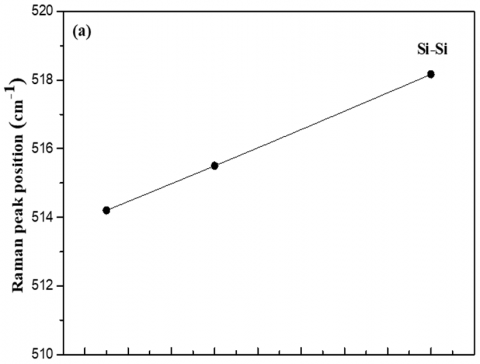
The dependencies of phonon frequencies on x are presented in Figure 4. It is evident that, the peak frequency of Si-Si (Ge-Ge) increases linearly with the Ge content, while the Si-Ge mode displays a nonlinear behaviour similar to that observed in the study [32].
(a) Si-Si; (b) Si-Ge and (c) Ge-Ge
The literature contains various empirical models for the Raman frequency shift dependence in SiGe alloys grown on bulk Si substrates, and each model may yield slightly different results.
The following experimental equations are introduced to determine the Si–Si, Ge-Ge and Si-Ge peaks position, denoted as $\omega_{S S}, \omega_{G G}$ and $\omega_{S G}$ in a SiGe layer:
$\omega_{S S}=\omega_0^{S i-S i}+a x$ (1a)
$\omega_{G G}=\omega_0^{G e-G e}+b x$ (1b)
$\omega_{\text {SiGe }}=\omega_0^{S i-G e}+f(x)$ (1c)
The constants a and b exhibit variations in the literature, with different authors reporting values ranging from -62 to -70.5 [33-36] for a and from 12.5 to 19.37 for b [33-35]. Additionally, the function f(x) can be a polynomial of first, second, or third order, as indicated in reference [37]. While $\omega_0^{S i-S i}, \omega_0^{G e-G e}$, and $\omega_0^{S i-G e}$ represent mode frequencies extrapolated to the limit as x approaches zero in SiGe alloys, the determined values are as follows: $\omega_0^{S i-S i}$ is 520.5±0.5 cm-1, $\omega_0^{G e-G e}$ is 280±1.5 cm-1, and $\omega_0^{S i-G e}$ is 400.3±0.2 cm-1[29, 32, 33].
Our experimental data fitting provides the following dependencies for Si-Si (Ge-Ge) modes:
$\omega_{S S}=511+26.5 x$ (2a)
$\omega_{G G}=286.5+59 x$ (2b)
On the contrary, when considering the Raman shift of the Si-Ge mode, we obtain:
$\omega_{\text {SiGe }}=366.7+466 x-109.5 x^2$ (2c)
Eq. (2) demonstrate a noteworthy level of precision when applied to the range of Ge content where 0 < x < 0.30, especially considering that the estimated measurement errors in our calculations consistently remain below 1%. These inaccuracies primarily stem from the challenges associated with precisely determining the peak positions of $\omega_{S S}, \omega_{G G}$ and $\omega_{S i G e}$ in our numerous spectra. This difficulty arises due to their relatively low intensity, particularly in the case of $\omega_{G G}$, as well as their substantial linewidths.
In our Raman spectroscopy results, we noticed an interesting pattern: as the Ge content increases in SiGe alloys, both the Si-Si mode and Ge-Ge mode show an increase in frequency. This observation can be attributed to multiple factors. Firstly, differences in bond lengths compared to pure Si and Ge play a role in these frequency variations. Secondly, structural disorder arises due to the random arrangement of Si and Ge atoms within the alloy. Additionally, the presence of mass disorder leads to an asymmetrical broadening and downward shift of both vibrational modes [32]. If there is a different behavior observed in SiGe alloys, such as the increase we have noted, it may be attributed to strain effects. Strain can introduce further modifications to the vibrational frequencies, influencing the behavior of the Si-Si and Ge-Ge modes. Specifically, the Si-Si mode exhibits a noticeable shift towards lower energies, with values falling below 520 cm-1, which is the typical Si substrate value. These negative shifts serve as confirmation of the tensile stress within these structures, which results from the relaxation process of the crystal structure in annealed DPSi substrate, mentioned above. Furthermore, the values of $\omega_0^{i-j}$ (with i or j representing Si or Ge) differ from those documented in previous studies [29, 32, 33], primarily due to the influence of strain on these vibrational frequencies.
Prior examinations utilizing Raman spectroscopy to study SiGe alloys have generated significant ambiguities regarding the relationships between alterations in Raman peak frequencies and stress. Furthermore, these investigations failed to establish accurate associations for the assessment of alloys within porous ma.terials. In the upcoming section, we will rigorously formulate a comprehensive set of equations for SiGe epilayers grown on annealed DPSi substrate.
In the literature, several sets of equations have been proposed that establish relationships between the frequencies of the Si-Si, Ge-Ge, and Si-Ge peaks, and Ge content as well as strain. These equations are typically presented in the following form [32]:
$\omega^{S i-S i}=\omega_0^{S i-S i}-A^{S i-S i} \chi+b^{S i-S i} \varepsilon_{/ /}$ (3a)
$\omega^{G e-G e}=\omega_0^{G e-G e}-A^{G e-G e} x+b^{G e-G e} \varepsilon_{/ /}$ (3b)
$\omega^{S i-G e}=\omega_0^{S i-G e}-A^{S i-G e} x+b^{S i-G e} \varepsilon_{/ /}$ (3c)
To solve the set of equations, we need to precisely determine the coefficients $A^{i-j}$ and $b^{i-j}$that relate the shift of Si-Si, Ge-Ge and Si-Ge vibrations to the Ge concentration and strain.
From Eqs. (3a) and (3b), we can extract $x$ and $\varepsilon_{/ /}$ as:
$x=\frac{\left(\omega_0^{S i-S i}-\omega^{S i-S i}\right) b^{G e-G e}+\left(\omega^{G e-G e}-\omega_0^{G e-G e}\right) b^{S i-S i}}{A^{G e-G e} b^{S i-S i}-A^{S i-S i} b^{S i-S i}}$ (4)
$\varepsilon_{/ /}=\frac{\left(\omega^{S i-S i}-\omega_0^{S i-S i}\right) A^{G e-G e}+\left(\omega^{G e-G e}-\omega_0^{G e-G e}\right) A^{S i-S i}}{A^{G e-G e} b^{S i-S i}-A^{S i-S i} b^{G e-G e}}$ (5)
$x$ and $\varepsilon_{/ /}$from Eqs. (4)-(5) are substituted in Eq. (3c) to obtain $\omega^{S i-G e}$. The $A^{i-j}$ coefficients are easily calculated where we have obtained $A^{S i-S i}=-26, A^{G e-G e}=-54$ and $A^{S i-G e}=-81$. The values of $\omega_0^{i-j}$ were extracted from Eq. (2).
The determination of the $b^{i-j}$ coefficients is more intricate as they relate to deformation and Raman frequency shifts. To calculate them, we employed the following equation [32, 38]:
$b^{i-j}=\frac{1}{2 \omega_0}\left(-\frac{2 C_{12}}{C_{11}} p+2 q\right)$ (6)
where, $C_{11}$ and $C_{12}$ are the elastic rigidity coefficients reported from the studies [39, 40], $p$ and $q$ are the deformation potentials of phonons and hither $\omega_0$ is the phonon frequency of unstrained cubic Si or Ge. Using values from the studies [39, 40], we have got $b^{S i-S i}=-811.5$ cm-1 and $b^{G e-G e}=-373$ cm-1.
To determine $b^{S i-G e}$, we have followed the method mentioned in references [32, 38]: first and from the set of Eq. (3), we have extracted:
$\Delta \omega_{e x p}^{S i-G e}=\omega_{e x p}^{S i-G e}-\omega_0^{S i-G e}=-A^{S i-G e} x+b^{S i-G e} \varepsilon_{/ /}$
with $A^{S i-G e}=-81$, then we have plotted $\Delta \omega_{\varepsilon_{/ /}}=\Delta \omega_{\text {exp }}^{S i-G e}-81 x$ versus the in-plane strain $\varepsilon_{/ /}$ in Figure 5. To that end, we have used strain values obtained by high resolution x-ray diffraction performed with an X'Pert PRO MRD Diffractometer and employing the following equation [9, 29]:
$\varepsilon_{\text {SiGe }}(\%)=\frac{a_{S i G e}^{\text {strain }}-a_{S i}}{a_{S i}} * 100$ (7)
where, $a_{\text {SiGe }}^{\text {strain }}$ is the lattice parameter for SiGe samples. The values measured are equal to 5.4932 Å, 5.5128 Å, and 5.5287 Å from 15% to 30% respectively.
The value of $b^{S i-G e}$ is obtained from the slope of linear curve in Figure 5, it yielded $b^{S i-G e}=-858.72 \mp 55$. This coefficient differs amply in litterature from -455 to -1040 cm-1 [38]. Many authors attribute this variability to the dependence of $b^{S i-G e}$ on $x$ [32,38].
Figure 5. $\Delta \omega_{\varepsilon / /}$ as a function of the in-plane strain $\varepsilon_{/ /}$
Considering the errors stemming from peak position inaccuracies, we arrived at the following set of equations that establish the relationship between the frequency shifts of the Si-Si, Ge-Ge and Si-Ge modes with respect to the Ge content (x) and the in-plane strain $\varepsilon_{/ /}$:
$\omega^{S i-S i}=\omega_0^{S i-S i}+26 x-811.5 \varepsilon_{/ /}$ (8a)
$\omega^{G e-G e}=\omega_0^{G e-G e}+54 x-373 \varepsilon_{/ /}$ (8b)
$\omega^{S i-G e}=\omega_0^{S i-G e}+81 x-858.7 \varepsilon_{/ /}$ (8c)
The computation of coefficients $\left(A^{i-j}\right.$ and $\left.b^{i-j}\right)$ is characterized by a high level of precision, typically yielding error bars of 1% or lower. Inaccuracies in Raman measurements primarily result from minor deviations in the peak positions of $\omega^{S i-S i}, \omega^{G e-G e}$ and $\omega^{S i-G e}$. The interplay between these phonon frequencies and their dependence on variables $\mathrm{x}$ and $\varepsilon_{/ /}$ has been established with remarkable accuracy.
Numerous research endeavors have been dedicated to investigating potential distortions in optical phonons within SiGe, with particular attention to the $b^{i-j}$ coefficients, which establish the connection between Raman frequency shifts and deformations. The estimated coefficients $b^{i-j}$ we obtained as a function of the deformation with the shift of:
Despite the low uncertainties associated with their determination, we have achieved a highly satisfactory outcome for these values, which demonstrate remarkable alignment with existing literature. Our derived set of equations showcases its versatility, extending applicability beyond the specified range (x < 0.35). However, it is crucial to emphasize that within this range, these equations exhibit exceptional precision.
Additionally, considering the set of equations obtained by measuring the experimental positions of the three phonon lines $\omega^{i-j}$ any combination of two out of the three equations enables the determination of the Ge content (x) and strain (ε) in the SiGe layer on the annealed DPSi substrate.
This achievement owes much to the invaluable contributions of Raman spectroscopy. It has facilitated the development of novel relationships linking Raman peak shifts to Ge content (x) and strain. As a result, these findings mark a significant milestone in the field, providing a robust foundation for the precise evaluation of strain and composition in SiGe alloys grown on PSi-based substrates.
Raman spectroscopy was conducted on SiGe membranes grown atop annealed DPSi substrate with x<0.35 in order to deduce the coefficients $A^{i-j}$ and $b^{i-j}$ that connect the frequency shifts of Si–Si, Si–Ge, and Ge–Ge vibrations to the Ge content (x) and strain. Accurate modeling of these frequency shifts yielded reliable estimates of $A^{i-j}$ and $b^{i-j}$. The determined coefficients $b^{i-j}$, which relate the Raman frequency shifts of Si–Si and Ge–Ge vibrations to deformation, were found to be -811.5 cm-1 and -373 cm-1, respectively. These vibrations exhibited a linear increase in frequency with increasing Ge content (x), while the behavior of the Si-Ge vibration followed a bell-shaped curve. The estimated coefficient $b^{S i-G e}$ was calculated by plotting the frequency variation against in-plane strain and was determined to be -858.7 cm-1.
Furthermore, all of these vibrations displayed sensitivity to strain, resulting in resonance frequency shifts. The observed strain in the SiGe epilayers was a direct consequence of the high annealing temperature applied to DPSi substrate, causing significant lattice structure expansion. This high-temperature annealing of DPSi substrate, generating unique tensile strain, not only impacts the lattice structure but also renders PSi an ideal substrate for heterogeneous system integration onto Si. This property makes it particularly well-suited for various applications in integrated systems.
Moreover, these vibrational modes enable the establishment of new relationships linking Raman peak shifts to both Ge content (x) and strain, crucial for a deeper understanding of strain distribution resulting from stress and composition variations. This knowledge is essential for expanding the range of applications for SiGe on annealed DPSi substrates, leveraging their full compatibility with CMOS technology.
The authors would like to thank the laboratory STM for providing the PSi samples.
[1] Eaglesham, D.J., Kvam, E.P., Maher, D.M., Humphreys, C.J., Bean, J.C. (2006). Dislocation nucleation near the critical thickness in GeSi/Si strained layers. Philosophical Magazine A, 59(5): 1059-1073. https://doi.org/10.1080/01418618908209837
[2] Paul, D.J. (1999). Silicon-germanium strained layer materials in microelectronics. Advanced Materials, 11(3): 191-204. https://doi.org/10.1002/(SICI)1521-4095(199903)11:3<191::AID-ADMA191>3.0.CO;2-3
[3] Hull, R., Bean, J.C., Eaglesham, D.J., Bonar, J.M., Buescher, C. (1989). Strain relaxation phenomena in GexSi1−x/Si strained structures. Thin Solid Films, 183(1-2): 117-132. https://doi.org/10.1016/0040-6090(89)90437-9
[4] Kasper, E., Lyutovich, K. (2004). Strain adjustment with thin virtual substrates. Solid-State Electronics, 48(8): 1257-1263. https://doi.org/10.1016/j.sse.2004.01.009
[5] Bogumilowicz, Y., Hartmann, J.M., Cherkashin, N., Claverie, A., Rolland, G., Billon, T. (2005). SiGe virtual substrates growth up to 50% Ge concentration for Si/Ge dual channel epitaxy. Material Sciences and Engineering B. 124–125: 113–117. https://doi.org/10.1016/j.mseb.2005.08.052
[6] Cecchi, S., Gatti, E., Chrastina, D., Frigerio, J., Müller Gubler, E., Paul, D.J., Guzzi, M., Isella, G. (2014). Thin SiGe virtual substrates for Ge heterostructures integration on silicon. Journal of Applied Physics. 115(9): 093502. https://doi.org/10.1063/1.4867368
[7] Berbezier, I., Ronda, A., Aqua, J., Favre, L., Frisch, T. (2014). SiGe nanostructures: From fundamental to applications. (2014). chapter 5. In book: Nanostructured Semiconductors. 165-245. https://dx.Doi.org/10.1201/B15634-6
[8] Magoariec, H., Danescu, A. (2009). Modeling macroscopic elasticity of porous silicon. Physica Statut Solidi C. 6(7): 1680–1684. https://doi.org/10.1002/pssc.200881053
[9] Gouder, S., Mahamdi, R., Aouassa, M., Escoubas, S., Favre, L., Ronda, A., Berbezier, I. (2014). Investigation of microstructure and morphology for the Ge on Porous Silicon/Si substrate hetero-structure obtained by Molecular Beam Epitaxy. Thin Solid Films, 550: 233-238. https://doi.org/10.1016/j.tsf.2013.10.183
[10] Poungoué Mbeunmi, A.B., El-Gahouchi, M., Arvinte, R., Jaouad, A., Cheriton, R., Wilkins, M., Valdivia, C.E., Hinzer, K., Fafard, S., Aimez, V., Ares, R., Boucherif, A. (2020). Direct growth of GaAs solar cells on Si substrate via mesoporous Si buffer. Solar Energy Materials and Solar Cells. 217: 110641. https://doi.org/10.1016/j.solmat.2020.110641
[11] Berbezier, I., Aqua, J.N., Aouassa, M., Favre, L., Escoubas, S., Gouye, A., Ronda, A. (2014). Accomodation of SiGe strain on a universally compliant porous silicon substrate. Physical Review B. 90(3): 035315-035320. https://doi.org/10.1103/PhysRevB.90.035315.
[12] Huang, Y.P., Zhu, S.Y., Li. A.Z., Wang. J., Huang, J.Y., Ye, Z.Z. (2001). Epitaxial growth of high-quality silicon films on double-layer porous silicon. Chinese Physics Letters. 18(11): 1507-1509. https://doi.org/10.1088/0256-307X/18/11/326
[13] Gardelis, S., Nassiopoulou, A.G., Mahdouani, M., Bourguiga, R., Jaziri, S. (2009). Enhancement and red shift of photoluminescence (PL) of fresh porous Si under prolonged laser irradiation or ageing: Role of surface vibration modes. Physica E: Low-dimensional Systems and Nanostructures. 41(6): 986-989. https://doi.org/10.1016/j.physe.2008.08.021
[14] Salonen, J., Mäkilä, E., Riikonen, J., Heikkila, T., Lehto, V.P. (2009). Controlled enlargement of pores by annealing of porous silicon. Physica status silidi (a). 206(6): 1313-1317. https://doi.org/10.1002/pssa.200881023
[15] Kuzma-Filipek, I., (2014). Sintering of Porous Silicon. Handbook of Porous Silicon, Springer International Publishing, Switzerland.
[16] Solanki, C.S., Bilyalov, R., Poortmans, J., Nijs., J., Mertens, R. (2004). Porous silicon layer transfer processes for solar cells. Solar Energy Materials and Solar Cells. 83(1): 101-113. https://doi.org/10.1016/j.solmat.2004.02.016
[17] Chiang., C.C., Lee, B.T.H. (2019). Annihilating pores in the desired layer of a porous silicon bilayer with different porosities for layer Transfer. Scientific Reports. 9(1): 12631-12639. https://doi.org/10.1038/s41598-019-49119-8
[18] Sahoo, M.K., Kale, P. (2019). Restructured porous silicon for solar photovoltaic: A review. Microporous and Mesoporous Materials. 289: 109619. https://doi.org/10.1016/j.micromeso.2019.109619
[19] Ott, N., Nerding, M., Müller, G., Brendel, R., Strunk, H.P. (2004). Evolution of the microstructure during annealing of porous silicon multilayers. Journal of Applied Physics, 95(2): 497–503. https://doi.org/10.1063/1.1633657
[20] Aouassa, M., Franzó, G., M’Ghaieth, R., Chouaib, H. (2021). Direct growth and size tuning of InAs/GaAs quantum dots on transferable silicon nanomembranes for solar cells application. Journal of Materials Science: Materials in electronics, 32: 18251–18263. https://link.springer.com/article/10.1007/s10854-021-06368-6
[21] Ramizy, A., Hassan, Z., Omar, K., Al-Douri, Y., Mahdi, M.A. (2011). New optical features to enhance solar cell performance based on porous silicon surfaces. Applied Surface Science, 257(14): 6112–6117. https://doi.org/10.1016/j.apsusc.2011.02.013
[22] Razali, N.S.M., Rahim, A.F.A., Radzali, R., Mahmood, A. (2017). Study of double porous silicon surfaces for enhancement of silicon solar cell performance. In AIP Conference Proceedings (Vol. 1885, No. 1). AIP Publishing.
[23] Jian-Jun, S., He-Ming, Z., Hui-Yong, H., Xian-Ying, D., Rong-Xi, X. (2007). Determination of conduction band edge characteristics of strained Si/Si1-xGex. Chinese Physics, 16(12): 3827-3831. https://doi.org/10.1088/1009-1963/16/12/045
[24] Pezzoli, F., Grilli, E., Guzzi, M., Sanguinetti, S., Chrastina, D., Isella, G., Von Kanel, H., Wintersberger, E., Stangl, J., Bauer, G. (2006). Strain-induced shift of phonon modes in Si1-xGex alloys. Materials Science in Semiconductor Processing, 9(4-5): 541-545. https://doi.org/10.1016/j.mssp.2006.08.046
[25] Hartmann, J.M., Baud, L., Rolland, G., Fabbri, J.M., Billon, T. (2006). Very high temperature growth of SiGe virtual substrates (15% < [Ge] < 45%). ECS Transactions, 3(7): 219-229. https://doi.org/10.1149/1.2355814
[26] Gouder, S. (2014). Nanostructures SiGe: Applications en microelectronique. Ph. D. Dissertation. Department of Electronic, Hadj Lakhdar University, Batna, Algeria.
[27] Zhang, S., Lu, Z.Y., Sheng, J., Gao, P.Q., Yang, X., Wu, S.D., Ye, J.C., Kambara, M. (2016). In situ annealing and high-rate silicon epitaxy on porous silicon by mesoplasma process. Applied Physics Express, 9(5): 055506. https://doi.org/10.7567/APEX.9.055506
[28] Bisi, O., Ossicini, S., Pavesi, L. (2000). Porous silicon: A quantum sponge structure for silicon based optoelectronics. Surface Science Reports, 8(1-3): 1–126. https://doi.org/10.1016/S0167- 5729(99)00012-6
[29] Perova, T.S., Wasyluk, J., Lyutovich, K., Kasper, E., Oehme, M., Rode, K., Waldron, A. (2011). Composition and strain in thin Si1-xGex virtual substrates measured by microRaman spectroscopy and X-ray diffraction. Journal of applied physics, 109(3): 033502. http://hdl.handle.net/2262/54844
[30] Groenen, J., Carles, R., Christiansen, S., Albrecht, M., Dorsch, W., Strunk, H.P., Wawra, H., Wagner, P. (1997). Phonons as probes in self-organized SiGe islands. Applied Physics Letter. 71(26): 3856-3858. https://doi.org/10.1063/1.120525
[31] Aouassa, M., Jadli, I., Slimen Hassayoun, L., Maaref, H., Panczer, G., Favre, L., Ronda, A., Berbezier, I. (2017). Analysis of composition and microstructures of Ge grown on porous silicon using Raman spectroscopy and Transmission Electron Microscopy. Superlattices and Microstructures. 112: 493-498. https://doi.org/10.1016/j.spmi.2017.10.003
[32] Rouchon, D., Mermoux, M., Bertin, F., Hartmann, J.M. (2014). Germanium content and strain in Si1-xGex alloys characterized by Raman spectroscopy. Journal of Crystal Growth. 392: 66-73. https://doi.org/10.1016/j.jcrysgro.2014.01.019.
[33] Tsang, J.C., Mooney, P.M., Dacol, F., Chu, J.O. (1994). Measurements of alloy composition and strain in thin GexSi1-x layers. Journal of Applied Physics, 75(12): 8098-8108. https://doi.org/10.1063/1.356554
[34] Pezzoli, F., Bonera, E., Grilli, E., Guzzi, M., Sanguinetti, S., Chrastina, D., Isella, G., von Känel, H., Wintersberger, E., Stangl, J., Bauer, G. (2008). Raman spectroscopy determination of composition and strain in Si1-xGex/Si heterostructures. Materials Science in Semiconductor Process, 11(5-6): 279-284. https://doi.org/10.1016/j.mssp.2008.09.012
[35] Capellini, G., De Seta, M., Busby, Y., Pea, M., Evangelisti, F., Nicotra, G., Spinella, C., Nardone, M., Ferrari, C. (2010). Strain relaxation in high Ge content SiGe layers deposited on Si. Journal of Applied Physics, 107: 063504. https://doi.org/10.1063/1.3327435
[36] Alonso, M.I., Winer, K. (1989). Raman spectra of c-Si1-xGex alloys. Physical Review B, 39(14): 10056. https://doi.org/10.1103/PhysRevB.39.10056
[37] Mala, S.A. (2015). Optical properties of strain-engineered multilayer Si/SiGe nanostructures. Ph.D. Dissertation. Helen and John C. Hartmann Department of Electrical and Computer Engineering, New Jersey Institute of Technology.
[38] Wong, L.H., Wong, C.C., Liu, J.P., sohn, D.K., Chan. L., Hsia, L.C., Zang, H., Ni, Z.H., Shen, Z.X. (2005). Determination of Raman phonon strain shift coefficient of strained silicon and strained SiGe. Japanese Journal of Applied Physics, 44(11): 7922–7924. https://doi.org/10.1143/JJAP.44.7922
[39] Anastassakis, E., Cantarero, A., Cardona, M. (1990). Piezo-Raman measurements and anharmonic parameters in silicon and diamond. Physical Review B, 41(11): 7529. https://doi.org/10.1103/PhysRevB.41.7529.
[40] Cerdeira, F., Pinczuk, A., Bean, J.C., Batlogg, B., Wilson, B.A. (1984). Raman scattering from GexSi1−x/Si strained-layer superlattices. Applied Physics Letters, 45(10): 1138–1140. https://doi.org/10.1063/1.95014
[41] Lockwood, D.J., Baribeau, J.M. (1992). Strain-shift coefficients for phonons in Si1−xGex epilayers on silicon. Physical Review B, 45(15): 8565. https://doi.org/10.1103/PhysRevB.45.8565.
[42] Shin, H.K., Lockwood, D.J., Baribeau, J.M. (2000). Strain in coherent-wave SiGe/Si superlattices. Solid State Communications. 114(10): 505-510. https://doi.org/10.1016/S0038-1098(00)00111-3