Mohammad A. Gharaibeh* | Aseel A. Almohammad
© 2022 IIETA. This article is published by IIETA and is licensed under the CC BY 4.0 license (http://creativecommons.org/licenses/by/4.0/).
OPEN ACCESS
This work introduces high-accuracy numerical solution for the two elastically coupled beams subjected to mechanical bending problem. Finite difference method (FDM) was considered to solve the governing equations along with the boundary conditions of the structure. The validity of this solution was ensured and tested with literature data. Finally, the influence of the key structural parameters of the problem, such as the relative stiffness between the beams as well as the elastic layer, was thoroughly discussed with the specific attention on its application in electronic assemblies subjected to mechanical bending. The numerical findings showed that for stiffer beams and compliant layer, the axial deformations of the layer are lower which can be reflected as lower solder stresses and hence more reliable designs of electronic devices.
coupled beams, finite difference method, electronic assemblies, mechanical bending
In service life, electronic devices are continuously prone to various mechanics bending, static and dynamic, loadings. For this reason, the assessment of bending-induced failures of electronic assemblies has become a major concern in industry. As a result, the reliability and quality of electronic structures have been widely and constantly investigated. Experimental works including, three-point bending tests [1], four-point bending tests [2, 3], vibration [4, 5] and drop impact [6, 7] were carried out for the evaluation of bending-related electronic assemblies’ reliability.
In addition to experiments, analytical solutions are very efficient and low-cost tools numerously used to evaluate the bending-induced stresses in electronic structures. A typical electronic package is made of a printed circuit board (PCB) and an integrated circuit (IC) component which both are connected, i.e., coupled, by an array of solder interconnects. This package-on-PCB structure has been widely treated in literature using the two elastically coupled beams problem. In this type of a problem, both the PCB and IC package are being modeled as two Euler-Bernoulli beams and the solder joints are treated as a thin elastic layer that couples and connects both beams.
Several successful attempts were made to solve this problem analytically. Perhaps the first work was done by Suhir [8] in which he developed a closed-form analytical solution to approximately compute solder axial stresses in electronic assemblies under static bending loading. In this solution, the solder joints were assumed to only deform axially and hence considered as axial discrete springs. The results of this approach were further applied to electronic assemblies under drop/impact conditions [9]. Wong et al. [10-12] presented approximate and accurate solutions of the same problem considering axial as well as flexural solder deformations in static [10, 11] and dynamic [12] bending loading conditions. Additionally, symmetric and non-symmetric bending cases were discussed [10, 11]. Pitarresi et al. [13] and Engle [14] obtained the solution of the coupled beams subjected to a central concentrated force problem. Later, Gharaibeh et al. [15] expanded the works of Pitarresi et al. [13] to solve for the case of partially coupled beams. Recently, Gharaibeh et al. [16] used the simple mechanics problem, the problem of a beam made of three materials, to solve for solder stresses. In the approach, solder stresses at the top and the bottom of the solder layer were computed. In addition to bending, the two elastically coupled beams has been widely adopted to solve for solder shear stresses due to thermal cycling loadings [17-26].
In 2016, Gharaibeh et al. [27] introduced the two elastically coupled plates for electronic assemblies’ vibrational problem. In this system, Ritz method was employed to solve for the system natural frequency, mode shapes and for solder nominal stresses. The findings of this solution were compared and correlated with experiments and with finite element analysis (FEA) data. Later, this solution was combined with design of experiment approaches to investigate the reliability of electronic assemblies under harmonic [28, 29] and random vibrations [30] as well as under shock loadings [31, 32].
The aim of this paper is to revisit the two elastically coupled beams problem and use the finite difference method (FDM) to solve the governing equation and to compute solder stresses. In this work, the cases of solder with only axial deformations as well as the case of solders with both axial and flexural deformations were studied. The FDM based solution was tested in terms of numerical accuracy and validated with literature data. Purposefully, this solution was used to examine the effect of the key structural parameters of the electronic assembly on solder stresses, hence, design recommendations were provided. The value of this solution is that it can be easily generalized to solve for any kind of loading and boundary conditions imposed on the coupled beams structure. Additionally, the method can be effectively expanded for the solution of the two-dimensional problem of the coupled plates structure.
We first start by the description of the coupled beams problem, the governing equations of the structure and the imposed loading and boundary conditions i section 2. Section 3, presents the details of the finite difference method scheme, an illustrative example, and numerical accuracy study is also introduced. The validation of this solution with literature data is presented in section 4 followed by the effect of the key structural parameters of coupled beams problem of solder stresses discussions.
This section fully describes the problem of the two elastically coupled beams in terms of problem assumptions, boundary conditions, and governing equation.
2.1 Problem definition
As mentioned previously, in the two elastically coupled beams model, the PCB and the IC component are designated as Euler-Bernoulli beams which both are elastically connected by a layer composed of evenly distributed springs. Here, the springs are considered to model the solder interconnect behavior. Figure 1 presents the details of this problem. As shown in this figure, the IC package is beam 1 and the PCB is beam 2. Considering both beams are of length (L), the bending, i.e., flexural, stiffness of beam 1 and beam 2 are D1 and D2, respectively. If the modulus of elasticity of the beam material is (E) and its cross-sectional moment of inertia is (I), then the flexural stiffness is D=EI. Hereinafter, the subscript 1 is used for beam 1 material and geometry (E1 and I1) and subscript 2 is for beam 2 characteristics (E2 and I2). Also, the transverse deflection functions of beam 1 and beam 2 are u1(x) and u2(x), respectively. For the modeling of solder joints, two analytical models were considered. The first and the simplest model treats the solders as linear springs with axial deformations only while the second, and most general, treats the interconnects as springs with both axial and flexural deformations.
Considering cylindrical-shapes solder of length (Ls) and cross-sectional area (As) as well as moment of inertia (Is) and made of a material with an elastic modulus (Es), the equivalent axial and bending stiffnesses are K=EsAs/Lsp2 and Km=EsLs/Lsp2, respectively, p is the pitch distance between two adjacent interconnects. For the case of axial deformations only, requires the presence of K only in the governing equation. However, in the case of axial and bending deformations, both K and Km are required.
Figure 1. Two elastically coupled beams problem
2.2 Governing equations
2.2.1 Solders with axial deformations
The governing differential equations of the coupled beams system with axial springs can be derived as [15]:
$D_{1} \frac{d^{4} u_{1}}{d x^{4}}=\sigma(x)$ (1.a)
$D_{2} \frac{d^{4} u_{2}}{d x^{4}}=-\sigma(x)$ (1.b)
where, the notation $d^{4} u / d x^{4}$ is the fourth derivative of the deflection functions; $\sigma(x)$ is the solder stress along the beam. Considering that the elastic layer of the springs follows the properties of Wrinkler foundation:
$\sigma(x)=K\left(u_{2}(x)-u_{1}(x)\right)$ (2)
By defining the solder, i.e., springs, axial deformation is the difference between beam 2 and beam 1 deflection, thus:
$\delta(x)=u_{2}(x)-u_{1}(x)$ (3)
Combining Eq. (1), Eq. (2) and Eq. (3), the governing equation of the solder axial deflection can be expressed as:
$\frac{d^{4} \delta}{d x^{4}}+4 \lambda_{1}^{4} \delta(x)=0$ (4)
where, $4 \lambda_{1}^{4}=K / D_{e}$, where De is the equivalent bending stiffness of beam 1 and beam 2 and defined as 1\De=1/D1+1/D2.
As stated earlier, for the case of springs with axial deformations, only K is appearing in the governing equation of Eq. (4) above.
2.2.2 Solders with axial as well as flexural deformations
In real-life systems, solder joints exhibit both axial and flexural (bending) deformations. In other words, the interconnects can be stretched as well as flexed. Therefore, for more accurate representation of the actual solder behavior, the flexing deformations must be considered. In this case, the governing equations of the coupled beams structure is [10]:
$D_{1} \frac{d^{4} u_{1}}{d x^{4}}=\sigma(x)-\frac{d M}{d x}$ (5.a)
$D_{2} \frac{d^{4} u_{2}}{d x^{4}}=-\sigma(x)+\frac{d M}{d x}$ (5.b)
where, M(x) is the distributed moment in the solder joint and expressed as [10]:
$M(x)=K_{m} \frac{d \delta}{d x}$ (6)
By combining Eq. (6), Eq. (5) and Eq. (3), the governing equation of the solder deformation, for this case, is written as:
$\frac{d^{4} \delta}{d x^{4}}-4 \lambda_{2}^{4} \frac{d^{2} \delta}{d x^{2}}+4 \lambda_{1}^{4} \delta(x)=0$ (7)
where, $4 \lambda_{2}^{4}=K_{m} / D_{e}$.
2.3 Boundary conditions
In structural mechanics point of view, loading and boundary conditions play an important rule in determining the behavior of any structural system. For simplicity, in the present analysis both beams are assumed to have simple supports (pin supports) at both ends $(x=0$ and $x=L)$. Additionally, an applied coupling moment $\left(M_{a}\right)$ is located at both ends of the structure. Thus, the boundary conditions of this system can be expressed as:
For Beam 1:
$u_{1}(0)=u_{1}(L)=0$ (8.a)
$\frac{d^{2} u_{1}}{d x^{2}}(x=0)=-\frac{M_{a}}{D_{1}}$ (8.b)
$\frac{d^{2} u_{1}}{d x^{2}}(x=L)=\frac{M_{a}}{D_{1}}$ (8.c)
For Beam 2:
$u_{2}(0)=u_{2}(L)=0$ (9.a)
$\frac{d^{2} u_{2}}{d x^{2}}(x=0)=-\frac{M_{a}}{D_{2}}$ (9.b)
$\frac{d^{2} u_{2}}{d x^{2}}(x=L)=\frac{M_{a}}{D_{2}}$ (9.c)
Considering Eq. (3), the boundary conditions for $\delta(x)$, are:
$\delta(0)=u_{2}(0)-u_{1}(0)=0$ (10.a)
$\delta(L)=u_{2}(L)-u_{1}(L)=0$ (10.b)
$\frac{d^{2} \delta(0)}{d x^{2}}=\frac{d^{2} u_{2}(0)}{d x^{2}}-\frac{d^{2} u_{1}(0)}{d x^{2}}=M_{a}\left(\frac{1}{D_{1}}-\frac{1}{D_{2}}\right)$ (10.c)
$\frac{d^{2} \delta(L)}{d x^{2}}=\frac{d^{2} u_{2}(L)}{d x^{2}}-\frac{d^{2} u_{1}(L)}{d x^{2}}=-M_{a}\left(\frac{1}{D_{1}}-\frac{1}{D_{2}}\right)$ (10.d)
The above boundary conditions (BC’s) of Eq. (10), were employed to solve for the case of solders with axial deformations only Eq. (4) as well as for the case of axial and flexural deformations Eq. (7).
3.1 Method implementation
In the present paper, finite difference method (FDM) was adopted to solve the boundary value problem of Eq. (4) and Eq. (7) along with the boundary conditions formulated in Eq. (10). In this numerical approach, the finite-divided-differences are substituted in the differential equations of Eq. (4) and Eq. (7). Thus, the linear ordinary differential equations (ODE’s) are transformed into a system of simultaneous linear algebraic equations than can be easily solved [33].
Starting with Eq. (4) solution, i.e., the case of axial deformations, the ODE here is of the fourth order. Hence, and according to FDM recommendations, a transformation to a system of two second order ODE’s is required. This can be easily done by letting $v(x)=d^{2} \delta / d x^{2}$, thus Eq. (4) can be re-written as a system of second order ODE’s as:
$v(x)=\frac{d^{2} \delta}{d x^{2}}$ (11.a)
$\frac{d^{2} v}{d x^{2}}=\frac{d^{4} \delta}{d x^{4}}=-4 \lambda_{1}^{4} \delta(x)$ (11.b)
For the second derivatives $d^{2} v / d x^{2}$ and $d^{2} \delta / d x^{2}$, the finite-divided-difference approximations are:
$\frac{d^{2} v}{d x^{2}}=\frac{v_{i+1}-2 v_{i}+v_{i-1}}{(\Delta x)^{2}}$ (12.a)
$\frac{d^{2} \delta}{d x^{2}}=\frac{\delta_{i+1}-2 \delta_{i}+\delta_{i-1}}{(\Delta x)^{2}}$ (12.b)
where, Δx is the step size and i=0, 1, 2, …, N-1 where N is the total number of nodes considered in the FDM solution. Hence $\Delta x=\frac{L}{N-1}$.
The approximations of Eq. (12) above can be substituted into Eq. (11) to give:
$v_{i+1}-2 v_{i}+v_{i-1}=-4(\Delta x)^{2} \lambda_{1}^{4} \delta_{i}$ (13.a)
$\delta_{i+1}-2 \delta_{i}+\delta_{i-1}=(\Delta x)^{2} v_{i}$ (13.b)
The equations above apply for each of the interior nodes of $v(x)$ and $\delta(x)$, as the first and the last nodes, i.e., the exterior nodes, are normally specified by the boundary conditions. Thus, the results system of linear algebraic equations will contain 2*(N-2) linear equations which will be tridiagonal. Such linear systems are very easy and computationally effective to solve. An illustrative example on the above-described procedure will be provided later.
To solve for the case of axial and bending deformations of the solder joints governed by Eq. (7), the same transformation procedure is required by letting $v(x)=d^{2} \delta / d x^{2}$, thus Eq. (7) becomes:
$v(x)=\frac{d^{2} \delta}{d x^{2}}$ (14.a)
$\frac{d^{2} v}{d x^{2}}=\frac{d^{4} \delta}{d x^{4}}=4 \lambda_{2}^{4} v(x)-4 \lambda_{1}^{4} \delta(x)$ (14.b)
Using the same procedure discussed in the previous paragraphs and with the implementation of Eq. (12), the finite difference form of Eq. (14) is:
$v_{i+1}-\left(2+4(\Delta x)^{2} \lambda_{2}^{4}\right) v_{i}+v_{i-1}=-4(\Delta x)^{2} \lambda_{1}^{4} \delta_{i}$ (15.a)
$\delta_{i+1}-2 \delta_{i}+\delta_{i-1}=(\Delta x)^{2} v_{i}$ (15.b)
Like the previous case of axial deformation only, the finite difference equations above apply for interior nodes. Also, the resultant system of tridiagonal linear equations will contain 2*(N-2) equations to solve, as it will be shown in the following subsection.
3.2 An illustrative example
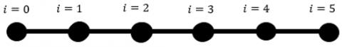
To show the details of the FDM along with an illustrative example, the most general case where both solder axial and bending deformations are available, was selected. If 6 nodes in total were chosen in this demonstration, 4 nodes are the interior nodes and 2 nodes are the exterior or boundary nodes. As shown in Figure 2, at i=0 and i=5 are node boundary nodes.
Figure 2. Six-node FDM system representation
The values of v(x) at such nodes are known and could be easily obtained, considering the BC’s of Eq. (10) as well as Eq. (11) and Eq. (13), as
$v_{0}=v(0)=\frac{d^{2} \delta(0)}{d x^{2}}=M_{a}\left(\frac{1}{D_{1}}-\frac{1}{D_{2}}\right)$ (16.a)
$v_{5}=v(L)=\frac{d^{2} \delta(L)}{d x^{2}}=-M_{a}\left(\frac{1}{D_{1}}-\frac{1}{D_{2}}\right)$ (16.b)
Also, the values of $\delta(x)$ at the boundary nodes are given by:
$\delta_{o}=\delta(0)=0$ (17.a)
$\delta_{5}=\delta(L)=0$ (17.b)
For the nodes at i=1, 2, 3, 4, the interior nodes, in the present FDM, two equations, one for v(x) and one for $\delta(x)$, per node are required and formulated. Hence, for the configuration studied in this illustrative example, 8 linear equations will be derived. It is important to emphasize here that in this configuration, 6 nodes were considered (N=6), however, only 4 nodes, or interior nodes, are being analyzed. Defining that n is the number of the interior nodes, thus n=N-2. Hence, for n interior nodes, the resultant set of linear equations will contain 2n number of equations. Here, n=4 and 8 equation will be derived.
To obtain the linear equations, considering Eq. (15) for i=1, 2, 3, 4, respectively, thus,
$-\left(2+4(\Delta x)^{2} \lambda_{2}^{4}\right) v_{1}+v_{2}+4(\Delta x)^{2} \lambda_{1}^{4} \delta_{1}=-M_{a}\left(\frac{1}{D_{1}}-\frac{1}{D_{2}}\right)$ (18.a.1)
$(\Delta x)^{2} v_{1}+2 \delta_{1}-\delta_{2}=0$ (18.a.2)
$v_{1}-\left(2+4(\Delta x)^{2} \lambda_{2}^{4}\right) v_{2}+v_{3}+4(\Delta x)^{2} \lambda_{1}^{4} \delta_{2}=0$ (18.b.1)
$(\Delta x)^{2} v_{2}-\delta_{1}+2 \delta_{2}-\delta_{3}=0$ (18.b.2)
$v_{2}-\left(2+4(\Delta x)^{2} \lambda_{2}^{4}\right) v_{3}+v_{4}+4(\Delta x)^{2} \lambda_{1}^{4} \delta_{3}=0$ (18.c.1)
$(\Delta x)^{2} v_{3}-\delta_{2}+2 \delta_{3}-\delta_{4}=0$ (18.c.2)
$v_{3}-\left(2+4(\Delta x)^{2} \lambda_{2}^{4}\right) v_{4}+4(\Delta x)^{2} \lambda_{1}^{4} \delta_{4}=M_{a}\left(\frac{1}{D_{1}}-\frac{1}{D_{2}}\right)$ (18.d.1)
$(\Delta x)^{2} v_{4}-\delta_{3}+2 \delta_{4}=0$ (18.d.2)
where, Δx=L/5. The 8 linear equations of Eq. (18) above can be written in a matrix form as:
$\left[\begin{array}{cccccccc}d_{1} & 0 & 0 & d_{2} & 0 & 0 & 0 \\ 1 & d_{1} & 1 & 0 & 0 & d_{2} & 0 & 0 \\ 0 & 1 & d_{1} & 1 & 0 & 0 & d_{2} & 0 \\ 0 & 0 & 1 & d_{1} & 0 & 0 & 0 & d_{2} \\ d_{3} & 0 & 0 & 0 & d_{4} & 0 & 0 & 0 \\ 0 & d_{3} & 0 & 0 & 0 & d_{4} & 0 & 0 \\ 0 & 0 & d_{3} & 0 & 0 & 0 & d_{4} & 0 \\ 0 & 0 & 0 & d_{3} & 0 & 0 & 0 & d_{4}\end{array}\right]\left\{\begin{array}{c}v_{1} \\ v_{2} \\ v_{3} \\ v_{4} \\ \delta_{1} \\ \delta_{2} \\ \delta_{3} \\ \delta_{4}\end{array}\right\}=\left\{\begin{array}{c}-M_{a}\left(\frac{1}{D_{1}}-\frac{1}{D_{2}}\right) \\ 0 \\ 0 \\ M_{a}\left(\frac{1}{D_{1}}-\frac{1}{D_{2}}\right) \\ 0 \\ 0 \\ 0 \\ 0\end{array}\right\}$ (19)
where, the diagonals are $d_{1}=-\left(2+4(\Delta x)^{2} \lambda_{2}^{4}\right), d_{2}=$ $4(\Delta x)^{2} \lambda_{1}^{4}, d_{3}=(\Delta x)^{2}$ and $d_{4}=2$.
The Eq. (19) above can be written in the compact form as:
$[A]\left\{V_{\delta}\right\}=\{c\}$ (20)
where, $[A],\left\{V_{\delta}\right\}$ and $\{c\}$ are the constants matrix, unknowns’ vector and the right-hand side (RHS) vector.
By solving the linear system of Eq. (20) as:
$\left\{V_{\delta}\right\}=[A]^{-1}\{c\}$ (21)
Thus, the solution for $v_{i}$ and $\delta_{i}$ for i=1, 2, 3, 4 can be obtained.
It is convenient to mention that if the case of solders with axial deformations was considered, the same procedure could be followed except for that in the coefficient’s matrix of Eq. (19) the diagonal $d_{1}$ becomes $d_{1}=-2$ while other diagonals $\left(d_{2}, d_{3}\right.$ and $\left.d_{4}\right)$ remains the same.
3.3 Numerical accuracy study
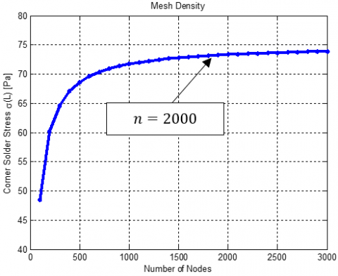
As any other numerical technique, FDM accuracy highly depends on the number of approximations, i.e., nodes, considered during the solution process. For this reason, a numerical accuracy study was conducted to optimize the numerical solution properties by achieving highest possible solution accuracy in minimal solution time. In the present accuracy study, several numbers of interior nodes (n) were tested. In each tested configuration, the solder stress at x=L, i.e., $\sigma(L)$, was computed, recorded, and hence plotted versus n. This is shown in Figure 3. In this analysis, it was concluded that at n=2000, or for 4000 equations, the $\sigma(L)$ has reached a converged asymptotic value. Therefore, this numerical configuration with n=2000 FDM interior nodes, or N=2002, was adopted throughout the analysis of this paper.
Figure 3. Numerical accuracy study details
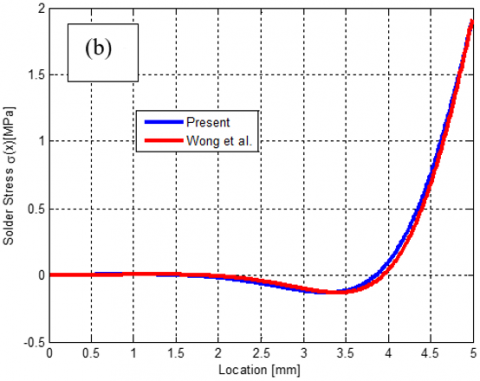
4.1 Numerical solution validation
The previously derived numerical solution was validated with literature data, specifically, with Wong et al. [11]. Wong’s data were based on a closed-form analytical solution of the coupled beams problem under symmetrical bending. Such results were thoroughly correlated with finite element analysis (FEA) finding. The key parameters in the present validation analysis, which were derived from Wong’s work, are D1=2083 N.mm, D2=2000 N.mm, K=9817 N/mm3 and Km=153 N/m2 for a structure of length L=10 mm, where the applied symmetrical moments is Ma=1 N.mm. This validation analysis was for solders with axial deformations only and for solders with both axial and flexural deformations. Also, as the problem possesses symmetry, only half the structure length was tested (0≤x≤5). The results of this study are shown in Figure 4. The figure shows that the present numerical solution agrees well with literature closed-form solution data, in both cases, for the whole length analyzed. Hence, a trust can be ensured in the results of the present numerical solution for both solder deformation cases.
Figure 4. Numerical solution validation with Wong et al. [10] data for (a) Solder with axial deformation and (b) solder with axial and flexural deformations
4.2 Parametric study
The previously optimized and validated numerical solution, for solder deformation schemes, was used to examine the effect of the key structural parameters of the coupled beam configuration on solder stresses. During this analysis, one key parameter was varied at a time while all other factors are held constant. Additionally, unless otherwise mentioned, for generalization a unity value was used for the geometric and/or material parameter as D1=1 N.m, D2=1 N.m, K=1 N/m3, Km=1 N/m2 and L=1 m. Also, the analysis was carried out for a unity applied coupling moment Ma=1 N.m as well. Besides, only half of the structure length (L/2≤x≤L) was plotted as the problem is highly symmetric.
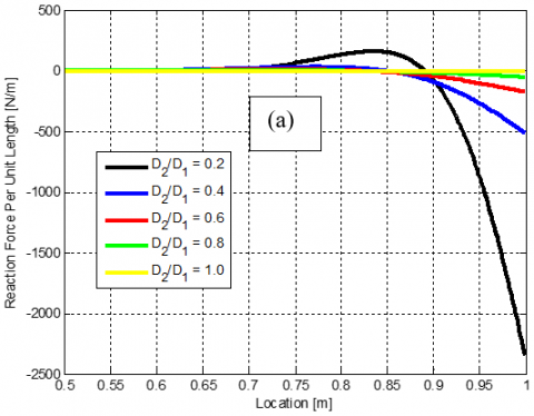
Figure 5. Effect of D2/D1 ratio on solder stress along the beam length (a) D2/D1 less than 1, (b) D2/D1 is between 1 and 2, (c) D2/D1 is greater than 2. Here solder deformations are only axial
4.2.1 Solder with axial deformations
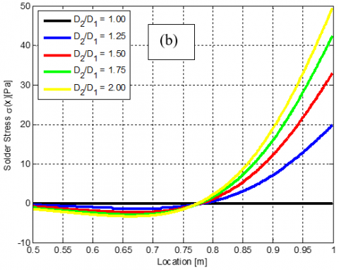
In this subsection, the case of solders with axial deformations only (Km=0) is considered. Practically, it is strongly believed that the relative stiffness between the PCB and the IC package (beam 2 to beam 1) has a significant and major effect on the solder stresses. Figure 5 shows the solder stresses along the elastic layer σ(x) at different D2/D1 values. In this figure, several scales of the stiffness ratio are tested for better observation.
The findings of this figure can be concluded as, for D2/D1 less 1.0 (Figure 5(a)), or for softer PCB compared to the IC package, the solder stresses are generally tensile stress for the range of 0.7L≤x≤0.9L. However, they become compressive stresses for x≥0.9 L and they are almost zero near the center of the electronic structure.
Besides, for much lower PCB stiffness with respect to the package, solder stresses become much higher. For D2/D1 between 1.0 and 2.0 (Figure 5(b)), or for almost equal stiffness of PCB and the IC component, things take a turn. Specifically, solder stresses are compressive 0.5L≤x≤0.8L and are tensile for x≥0.8L.
Additionally, for little higher bending stiffness ratio, solder stress rises slightly. A common observation in Figure 5(a) and Figure 5(b), for an equal PCB and package stiffness (D2/D1=1), solder stresses are equal to zero, as the relative deflection between the PCB and the component vanishes. This can be mathematically observed as the boundary conditions of Eq. (10) go to zero, hence no loading is applied.
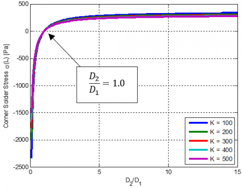
For much larger bending stiffness ratios, shown in Figure 5(c), solder stresses are still compressive for 0.5L≤x≤0.7L, and tensile near the edges (x≥0.8L) of the structure. Again, for stiffer PCB systems, solder stresses are rising accordingly. However, the effect of D2/D1 vanishes for very high PCB stiffness, with respect to the package stiffness, or for D2/D1≥4.0. One more important result from Figure 5, is that for all D2/D1 ratios, the maximum solder stress occurs at the edge of the structure or at x=L=1.0. Such maximum solder stresses are investigated closely in Figure 6. In this figure, solder stresses at x=L or σ(L) are plotted versus the D2/D1 ratios for several solder layer stiffness (K) values.
Figure 6. Solder maximum stress as a function of D2/D1 ratio at different solder stiffness systems
The results of this figure states that solder maximum stresses for compliant PCB structures (D2/D1<1), are very high compressive stresses. However, for stiffer PCB’s, maximum tensile stresses are much lower and the effect of D2/D1 ratio diminishes for D2/D1>3.0, for any solder stiffness configuration. Thus, the present paper recommends the use of relatively stiff circuit board structure, compared to IC package, for lower solder stresses and hence for longer fatigue life, or service life, for electronics in mechanical bending loading environments.
Figure 7 presents the effect of the solder stiffness on corner solder stresses at several D2/D1 ratios. The results here states that maximum solder stresses are proportional solder stiffness and for the case of solders with axial deformations only, the effect is linear. Again, for compliant PCB’s solder stresses are very high compressive stresses while for stiffer boards the solder stresses are lower and are tensile in nature. For this reason, the present work recommends the use of relatively compliant solder configurations in electronic devices prone to mechanical bending for longer service life of the electronic system.
4.2.2 Solders with Both Axial and Flexural Deformations
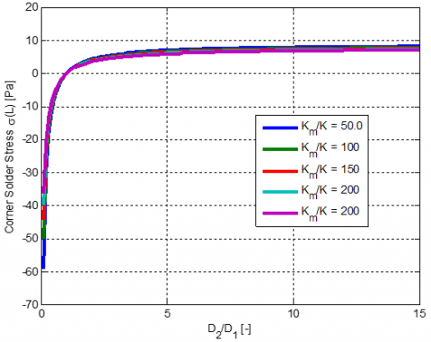
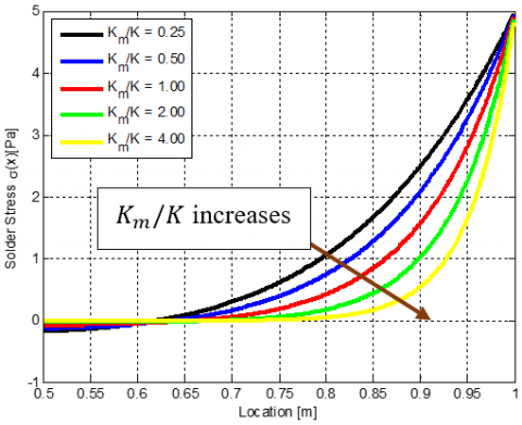
Here, the effect of solder bending stiffness is considered (Km≠0) in the analysis. Figure 8 depicts the effect of D2/D1 ratios on solder stress along the coupled beams length. Similar results of Figure 5 were observed. Specifically, for compliant PCB systems, solder stresses are high and compressive. Additionally, for stiff PCB’s, solder stresses get tensile and lower. Besides, for much higher bending stiffness ratios, solder stresses reach a constant value. This effect holds true even for several solder bending stiffness to axial stiffness (Km/K) configurations, as shown in Figure 9.
Figure 7. Effect of solder axial stiffness on the maximum stresses of the corner solder interconnect
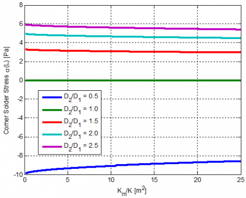
The effect of Km/K on solder maximum stress is plotted in Figure 10. Here, in contrast to Figure 7, the effect of solder bending to axial stiffness ratio is inversely proportional and the effect is nonlinear. In other words, for higher Km/K ratios, corner solder stresses are becoming lower. This can be mathematically discussed by dividing solder bending stiffness $\left(K_{m}=E_{s} I_{s} / L_{s} p^{2}\right)$ by solder axial stiffness $\left(K=E_{s} A_{s} / L_{s} p^{2}\right)$, thus:
$\frac{K_{m}}{K}=\frac{I_{S}}{A_{S}}$ (22)
Remembering the definition of the radius of gyration ($r_{g}$) of a given section:
$r_{g}=\sqrt{\frac{I_{s}}{A_{s}}}=\sqrt{\frac{K_{m}}{K}}$ (23)
Instead of researching each solder joint cross-section related parameter, it is now more convenient to only test the cross section radius of gyration. In mechanics point of view, is used to describe the distribution of cross sectional area in a column, i.e. solder, around its centroidal axis with the mass of the body. Generally, it is another measurement too for the structure stiffness.
Figure 8. Effect of D2/D1 ratio on solder stress along the beam length (a) D2/D1 less than 1, (b) D2/D1 is between 1 and 2, (c) D2/D1 is greater than 2. Here solder deformations are both axial and flexural
Figure 9. Solder maximum stress as a function of D2/D1 ratio at different solder bending to axial stiffness ratios
Figure 10. Effect of solder bending to axial stiffness on the maximum stresses of the corner solder interconnect
Figure 11. Effect of solder bending to axial stiffness on the solder stresses along the length of the electronic assembly
Thus, for a solder with a cross-section of a relatively large radius of gyration, solder stresses are slightly lower. In structural mechanics point of view, radius of gyration describes the distribution of a cross-sectional area around its centroidal axis. Thus, for larger radius of gyration values, solders become stiffer geometrically, which results in higher solder resistance for deformations, strains, and stresses, accordingly. A similar behavior was observed in Figure 11. This figure shows lower solder stresses along the coupled beams length for larger solder bending to axial stiffness ratio.
Based on the previous discussions, the present paper highly recommends the geometric design of solders to have large cross-sectional radius of gyration configurations for lower solder stresses and hence, longer fatigue and service solder life.
This paper presented an accurate numerical solution for the analysis of the two elastically coupled beams problem using the finite difference method. In this study, two cases were discussed, solders with axial deformations only and solders with both axial as well as flexural deformations. In this solution, the numerical accuracy was ensured, and the results of this solutions were validated with literature data, for both cases studied. Finally, the effect of the key geometric and material parameters of the coupled beams system on solder stresses was thoroughly investigated. As a result, the present work recommends the design of electronic assemblies with stiffer printed circuit board configurations as well as the design of solder interconnects with relatively large radius of gyration to reduce the bending-induced solder stresses and hence prolonged service life.
|
$D_{1}, D_{2}$ |
Flexural rigidity of top, bottom beams (N. $m^{2}$) |
|
$D_{e}$ |
Effective flexural rigidity of top and bottom beams (N. $m^{2}$) |
|
$K, K_{m}$ |
Axial, flexural stiffness of the elastic layer |
|
L |
Beam length (m) |
|
$M_{a}$ |
Applied bending moment (N.m) |
|
$M(x)$ |
Distributed reaction moment in the elastic layer |
|
$u_{1}(x), u_{2}(x)$ |
Deflection of top, bottom beams |
|
Greek symbols |
|
|
$\sigma(x)$ |
Solder axial stresses (Pa) |
|
$\delta(x)$ |
Solder axial deflections (m) |
|
$\lambda_{1}, \lambda_{2}$ |
Partial differential equations dimensionless constants |
[1] Lau, D., Chan, Y.S., Lee, S.R., Fu, L., Ye, Y., Liu, S. (2006). Experimental testing and failure prediction of PBGA package assemblies under 3-point bending condition through computational stress analysis. In 2006 7th International Conference on Electronic Packaging Technology, pp. 1-7. https://doi.org/10.1109/ICEPT.2006.359865
[2] Che, F.X., Pang, H.L.J., Zhu, W.H., Sun, A.Y. (2006). Cyclic bend fatigue reliability investigation for Sn-Ag-Cu solder joints. In 2006 8th Electronics Packaging Technology Conference, pp. 313-317. https://doi.org/10.1109/EPTC.2006.342735
[3] Chea, F.X., Pang, J.H.L. (2006). Modeling board-level four-point bend fatigue and impact drop tests. In 56th Electronic Components and Technology Conference. https://doi.org/10.1109/ECTC.2006.1645684
[4] Su, Q., Pitarresi, J., Gharaibeh, M., Stewart, A., Joshi, G., Anselm, M. (2014). Accelerated vibration reliability testing of electronic assemblies using sine dwell with resonance tracking. In 2014 IEEE 64th Electronic Components and Technology Conference (ECTC), pp. 119-125. https://doi.org/10.1109/ECTC.2014.6897276
[5] Su, Q.T., Gharaibeh, M.A., Stewart, A.J., Pitarresi, J.M., Anselm, M.K. (2018). Accelerated vibration reliability testing of electronic assemblies using sine dwell with resonance tracking. Journal of Electronic Packaging, 140(4): 041004. https://doi.org/10.1115/1.4040923
[6] Gharaibeh, M., Pitarresi, J., Anselm, M. (2013). Strain correlation: Finite element modeling and experimental data. Universal Instruments Advanced Research in Electronic Assemblies Consortium, Conklin, NY, pp. 12-13.
[7] Gharaibeh, M., Su, Q., Pitarresi, J., Anselm, M. (2013). Board level drop test: Comparison of two ANSYS modeling approaches and correlation with testing. Universal Instruments Area Consortium.
[8] Suhir, E. (1988). On a paradoxical phenomenon related to beams on elastic foundation: Could external compliant leads reduce the strength of a surface-mounted device? Journal of Applied Mechanics, 55(4): 818-821. https://doi.org/10.1115/1.3173727
[9] Wong, E.H., Mai, Y.W. (2006). New insights into board level drop impact. Microelectronics Reliability, 46(5-6): 930-938. https://doi.org/10.1016/j.microrel.2005.07.114
[10] Wong, E. H., Mai, Y.W., Seah, S.K.W., Lim, K.M., Lim, T.B. (2006). Analytical solutions for interconnect stress in board level drop impact. In 56th Electronic Components and Technology Conference 2006, p. 8. https://doi.org/10.1109/ECTC.2006.1645905
[11] Wong, E.H., Mai, Y.W., Seah, S.K., Lim, K.M., Lim, T.B. (2007). Analytical solutions for interconnect stress in board level drop impact. IEEE Transactions on Advanced Packaging, 30(4): 654-664. https://doi.org/10.1109/TADVP.2007.898599
[12] Wong, E.H., Wong, C.K. (2009). Approximate solutions for the stresses in the solder joints of a printed circuit board subjected to mechanical bending. International Journal of Mechanical Sciences, 51(2): 152-158. https://doi.org/10.1016/j.ijmecsci.2008.12.003
[13] Pitarresi, J.M., Ceurter, J., Schifter, J., Engel, P.A. (1999). Elasticly coupled beams loaded by a point force. In 13th Engineering Mechanics Conference, Baltimore, MD.
[14] Engel, P.A. (1990). Structural analysis for circuit card systems subjected to bending. Journal of Electronic Packaging, 112(1): 2-10. https://doi.org/10.1115/1.2904336
[15] Gharaibeh, M.A., Liu, D., Pitarresi, J.M. (2017). A pair of partially coupled beams subjected to concentrated force. IEEE Transactions on Components, Packaging and Manufacturing Technology, 7(8): 1293-1304. https://doi.org/10.1109/TCPMT.2017.2670019
[16] Gharaibeh, M.A., Ismail, A.A., Al-Shammary, A.F., Ali, O.A. (2019). Three-material beam: Experimental setup and theoretical calculations. Jordan Journal of Mechanical & Industrial Engineering, 13(4). http://jjmie.hu.edu.jo/vol-13-4/65-19-01.pdf.
[17] Suhir, E. (1986). Stresses in bi-metal thermostats. Journal Applied Mechanics (Trans. ASME), 53(3): 657-660. https://doi.org/10.1115/1.3171827
[18] Suhir, E. (1988). An approximate analysis of stresses in multilayered elastic thin films. ASME Journal Applied Mechanics, 55(1988): 143-148.
[19] Suhir, E. (1989). Interfacial stresses in bimetal thermostats. ASME Journal Applied Mechanics, 56(1989): 595-600.
[20] Suhir, E. (2001). Analysis of interfacial thermal stresses in a trimaterial assembly. Journal of Applied Physics, 89(7): 3685-3694.
[21] Suhir, E., Shangguan, D., Bechou, L. (2013). Predicted thermal stresses in a trimaterial assembly with application to silicon-based photovoltaic Module. Journal of Applied Mechanics, 80(2). https://doi.org/10.1115/1.4007477
[22] Wong, E.H., Wong, C.K. (2008). Tri-layer structures subjected to combined temperature and mechanical loadings. IEEE Transactions on Components and Packaging Technologies, 31(4): 790-800. https://doi.org/10.1109/TCAPT.2008.2001196
[23] Wong, E.H., Lim, K.M., Mai, Y.W. (2009). Analytical solutions for PCB assembly subjected to mismatched thermal expansion. IEEE Transactions on Advanced Packaging, 32(3): 602-611. https://doi.org/10.1109/TADVP.2009.2025222
[24] Wong, E.H. (2015). Interfacial stresses in sandwich structures subjected to temperature and mechanical loads. Composite Structures, 134: 226-236. https://doi.org/10.1016/j.compstruct.2015.07.106
[25] Wong, E.H. (2016). Design analysis of sandwiched structures experiencing differential thermal expansion and differential free-edge stretching. International Journal of Adhesion and Adhesives, 65: 19-27. https://doi.org/10.1016/j.ijadhadh.2015.10.021
[26] Wong, E.H., Liu, J. (2017). Interface and interconnection stresses in electronic assemblies–A critical review of analytical solutions. Microelectronics Reliability, 79: 206-220. https://doi.org/10.1016/j.microrel.2017.03.010
[27] Gharaibeh, M.A., Su, Q.T., Pitarresi, J.M. (2016). Analytical solution for electronic assemblies under vibration. Journal of Electronic Packaging, 138(1). https://doi.org/10.1115/1.4032497
[28] Gharaibeh M., (2018). Reliability assessment of electronic assemblies under vibration by statistical factorial analysis approach. Soldering & Surface Mount Technology, 30(3): 171-181. https://doi.org/10.1108/SSMT-10-2017-0036
[29] Gharaibeh, M.A. (2018). Reliability analysis of vibrating electronic assemblies using analytical solutions and response surface methodology. Microelectronics Reliability, 84: 238-247. https://doi.org/10.1016/j.microrel.2018.03.029
[30] Gharaibeh, M.A., Pitarresi, J.M. (2019). Random vibration fatigue life analysis of electronic packages by analytical solutions and Taguchi method. Microelectronics Reliability, 102: 113475. https://doi.org/10.1016/j.microrel.2019.113475
[31] Gharaibeh, M.A., Su, Q.T., Pitarresi, J.M. (2018). Analytical model for the transient analysis of electronic assemblies subjected to impact loading. Microelectronics Reliability, 91: 112-119. https://doi.org/10.1016/j.microrel.2018.08.009
[32] Gharaibeh, M.A. (2020). Analytical solutions for electronic assemblies subjected to shock and vibration loadings. In Handbook of Materials Failure Analysis, 179-203.
[33] Chapra, S.C., Canale, R.P. (2010). Numerical Methods for Engineers., McGraw-Hill Higher Education Boston, MA, USA.