Abdelhamid Lechlech | Djamel Kalaidji | Mohammed Salim Hadjidj | Jamel Baili* | Hanaa Abu-Zinadah | Giulio Lorenzini | Hijaz Ahmad | Younes Menni
© 2021 IIETA. This article is published by IIETA and is licensed under the CC BY 4.0 license (http://creativecommons.org/licenses/by/4.0/).
OPEN ACCESS
In industry, it is important to measure the voltage and the electric field as they are indispensable in the design of insulation systems which allow detecting voltage problems (insufficient voltage, voltage drop, voltage distortion, voltage cut-off, etc.), despite the high performance of advanced numerical calculation methods that exist today, which unfortunately are still unable to estimate the distribution of the disturbed electric field in the presence of space charges. Indeed, the distribution of space charges (a cloud of electrons, located in a space that may be vacuum, gas, liquid or solid that can impede the displacement of the flow of circulating electrons) depends on factors such as the mobility of charged particles and the ionization rate of gaseous molecules. Therefore, it is necessary to accurately measure the intensity of the electric field in order to obtain more efficiency and reliability of the operations in high voltage systems. The development of nanotechnology, microelectronics and integrated optics (all optical components are combined on a single support) led to the birth of optical electric field sensors. Electric field sensors using the E/O effect fall into two categories, namely low-field sensors and high-field sensors. In this context, the present work focuses on the optical and electro-optical properties of the material used. The configurations and geometric shapes are studied in order to choose the most appropriate ones for various applications.
optical electric-field sensor, optical waveguide sensor, dielectric sensors, electro-optic effect, signal propagation, wave behavior, wave propagation, transmittance of guides, Reflectance of guides, guide’s length, detection, crystal, nanotechnology
Nanosciences and nanotechnologies can be defined as the set of studies and processes used in the fabrication and manipulation of structures (electronic, chemical, etc.), devices and hardware systems, at the nanometer scale. Having grown rapidly during the last two decades, and successfully synthesized the achievements of physics, chemistry, life science as well as information and computational science and technology, nanoscience and nanotechnology have emerged as interdisciplinary fields of modern science and technology with various prospective applications towards environmental protection and the sustainable development of industry, agriculture, public health etc. [1] Thus, nanosciences concern the study of phenomena and the manipulation of matter at atomic, molecular and macromolecular scales, where the properties differ slightly from those that prevail at a larger scale. However, nanotechnologies concern the design, characterization, production and application of structures, devices and systems through the control of shape and size, at the nanometric scale.
The purpose of this work is to present, in a general way, the basic elements needed in the realization of optoelectronic sensors. First, the optical and electro-optical properties of the materials are studied. Next, the main applications of optoelectronics are investigated, and the various stages involved in the production process, with the main families of sensors, are described. Then, the basic principles of radiometry as well as the relationships between radiometric quantities are reported. After that, our work focuses on the diffusion of radiation and on the role that optics may play in the calculation of the flux of the optical signal received by the detector which then converts it into an electrical signal [2]. The combination of some electronic and optical words led to the creation of various names and applications. A material is said to be electro-optical if its optical properties (transmission, refractive index, and birefringence) are modifiable under the action of an electric field.
The Pockels effect is the appearance of birefringence in an environment created by a static or variable electric field [3]. Birefringence is proportional to the electric field, but the Kerr effect is proportional to the square of this same field. The Pockels effect appears only in crystals having no symmetry with respect to an axis; such crystals may be lithium niobate or gallium arsenide [4].
The optical properties (such as the refractive index) of an anisotropic dielectric environment (such as the crystalline) depend on the propagation direction of the electromagnetic wave that passes through the environment studied. For a given (fixed) propagation direction, there are two refractive indices which are associated with electromagnetic waves having polarization states that enable them to propagate without alteration [5].
A wave propagating in any direction can be decomposed into two independent linear waves, having linear wave propagation modes. Each one of the two main components of the wave will have a refractive index; their difference Δn is called the natural birefringence of the environment in the direction under consideration.
Birefringence means that there are two refractive indices or two propagation directions for each incident ray [6]. An electromagnetic wave is represented by the data related to its two vectors, namely the electric field $\vec{E}$ and the magnetic field $\vec{H}$. The influence of these fields on the material results in the introduction of two other vectors, the electric displacement vector $\vec{D}$ and the magnetic induction vector $\vec{B}[7,8]$.
In a nonmagnetic material medium (crystalline medium), the vector fields are related to each other by Maxwell’s equations which are written as follows:
$\overrightarrow{\operatorname{rot}} \vec{E}=\frac{-\partial \vec{B}}{\partial t}, \operatorname{div} \vec{B}=0, \overrightarrow{\operatorname{rot}} \vec{H}=\frac{\partial \vec{D}}{\partial t}, \operatorname{div} \vec{D}=0$ (1)
In addition to Maxwell’s equations, the electric field E and the magnetic field B must satisfy:
The constitutive relationship (regardless of the optical activity)
$D=\varepsilon_{0} \cdot[\varepsilon] . E$ (2)
The energy conservation law, which is checked by the electromagnetic energy density:
$\left\{\begin{array}{c}w=w_{e}+w_{m} \\ w_{e}=1 / 2 \cdot E \cdot D \\ w_{m}=1 / 2 \cdot B \cdot H \\ S=E * H \ldots \text { POYNTING vector }\end{array}\right.$ (3)
$\frac{d w}{d t}+\operatorname{div} S=0$ (4)
This allows deducing the relative permittivity tensor $\varepsilon$ which, in addition to being symmetric, depends only on six (6) independent parameters:
$\varepsilon=\left[\begin{array}{lll}\varepsilon_{11} & \varepsilon_{12} & \varepsilon_{13} \\ \varepsilon_{12} & \varepsilon_{22} & \varepsilon_{23} \\ \varepsilon_{13} & \varepsilon_{23} & \varepsilon_{33}\end{array}\right]$ (5)
By a simple axis change, it becomes possible to transform a real symmetric tensor into a real diagonal tensor expressed in a Cartesian coordinate system, also referred to as the proper coordinate system of the material medium. The coordinate axes of this coordinate system are the proper or main axes of the medium considered. The relationship then becomes:
$\left[\begin{array}{l}D_{x} \\ D_{y} \\ D_{z}\end{array}\right]=\left[\begin{array}{ccc}\varepsilon_{x} & 0 & 0 \\ 0 & \varepsilon_{y} & 0 \\ 0 & 0 & \varepsilon_{z}\end{array}\right]\left[\begin{array}{l}E_{x} \\ E_{y} \\ E_{z}\end{array}\right]$ (6)
Searching for such a coordinate system is made easy by the symmetry elements of the crystal structure of the material. Three (3) coefficients $\left(\varepsilon_{x}, \varepsilon_{y}, \varepsilon_{z}\right)$ are thus necessary for the characterization of any anisotropic medium; their relative values allow for the classification of the optical media.
Once the tensor is diagonalized [9] it becomes possible, by analogy with isotropic media, to introduce the refractive indices $n_{x}, n_{y}, n_{z}$, which are related to the permittivities through the relation $\varepsilon_{i}=n_{i}^{2}(\mathrm{i}=\mathrm{x}, \mathrm{y}, \mathrm{z})$. These indices are called the main refractive indices of the optical environment under consideration $[10]$. When the environment studied is subjected to an electric field, it is important to understand the behavior of its refractive indices during the development operation an optical electric field sensor.
Therefore, it is important to characterize the relationships that link these indices to the electric field. This allows us to define the index ellipsoid.
In the absence of an electric field, the index ellipsoid maybe described by the following general equation [11]:
$\sum_{i j} \eta_{i j} x_{i}, x_{j}=1$ (7)
where, $\eta_{i j}=\frac{1}{\varepsilon_{i j}}$ is the electric impermeability tensor. In the proper coordinate system, the equation becomes:
$\frac{x^{2}}{n_{11}^{2}}+\frac{y^{2}}{n_{22}^{2}}+\frac{z^{2}}{n_{33}^{2}}=1$ (8)
Using the contracted Voigt notation, which allows transforming the pairs of indices (i, j) into a simple index p, one gets this Table 1 & 2:
Table 1. Voigt notation
|
(i, j) |
(1, 1) |
(2, 2) |
(3, 3) |
|
p |
1 |
2 |
3 |
Table 2. Continued
|
(i, j) |
(2, 3) (3, 2) |
(1, 3) (3, 1) |
(1, 2) (2, 1) |
|
p |
4 |
5 |
6 |
Therefore:
$\frac{x^{2}}{n_{11}^{2}}+\frac{y^{2}}{n_{22}^{2}}+\frac{z^{2}}{n_{33}^{2}}=1 \Rightarrow \frac{x^{2}}{n_{x}^{2}}+\frac{y^{2}}{n_{y}^{2}}+\frac{z^{2}}{n_{z}^{2}}=1$ (9)
In this case, the three (3) axes $\mathrm{x}, \mathrm{y}$, z represent the main axes of the crystal and $n_{x}, n_{y}, n_{z}$ are the corresponding refractive indices.
The index ellipsoid (indicator) allows for a simple geometrical representation of the optical properties of anisotropic crystals; it also helps to determine the refractive indices along a well-defined propagation direction of a light wave. Figure 1 represents a general index ellipsoid. The main axes X, Y, $Z$ have the following lengths: $2 n_{x}, 2 n_{y}, 2 n_{z}$.
Figure 1. Index ellipsoid
The random section is a plane that passes through the origin and is perpendicular to a light beam propagating in an arbitrary direction $\overline{O P}$. The intersection of this plane with the ellipsoid is an ellipse. In the case of uniaxial crystals, one obtains an ellipsoid of revolution about the axis OZ which is the optical axis of the crystal. Then, the general equation of the ellipsoid becomes:
$\frac{x^{2}+y^{2}}{n_{o}^{2}}+\frac{z^{2}}{n_{e}^{2}}=1$ (10)
$\mathrm{n}_{0}$ : ordinary refractive index.
$n_{e}$ : extraordinary refractive index which is in the direction of the optical axis.
The index ellipsoid represents the indicator surface of the tensor [ε] [12]. It allows a simple determination of the propagation eigenstates. This ellipsoid appears as the fundamental surface in studying anisotropies induced by external fields. Indeed, the index ellipsoid changes slightly under the action of an electric field and the new optical properties of the crystal under pressure can then be deduced.
An induced polarization appears in any material subjected to an incident electromagnetic wave [13]. This polarization determines the complete response of a medium to the excitation radiation. For example, the high luminous intensities emitted by lasers produce electric fields with magnitude close to that of the electric field ensuring the cohesion of electrons. This would produce the optical non-linearity within the dielectric environment [14].
In general, the dielectric properties of a material are affected when it is subjected to an electromagnetic field.
Indeed, a birefringence is induced in an isotropic material, but in an anisotropic material, the birefringence is modified (or altered) [15].
The electro-optical effect induces a variation of the dielectric constant. In addition, an axis of rotation is observed within the crystal that is subjected to an electric field. The electric field induces an index ellipsoid deformation.
The most widely used materials, showing a linear electro-optic effect, are those whose E / O coefficients are optimal and their other characteristics are compatible. Lithium niobate was then selected to be used in this study [16].
4.1 Material Presentation
Lithium niobate is an oxygen-octahedra ferroelectric material [17]. It has only one structural phase transition at the temperature $\mathrm{T}_{\mathrm{C}} \approx 1200{ }^{\circ} \mathrm{C}$. Beyond that temperature, in its para-electric phase, this material becomes centro-symmetric. Below $\mathrm{T}_{\mathrm{C}}$, and at ambient temperature, it is ferroelectric with a rhombohedral (trigonal) symmetry $\mathrm{C}_{3 \mathrm{~V}}=3 \mathrm{~m}$. It has a third order polar axis. It is manufactured in such a way that it is mono-domain.
Lithium niobate is a negative uniaxial material, with $\mathrm{n}_{\mathrm{e}}<\mathrm{n}_{\mathrm{o}}$. It has a large spontaneous polarization $\mathrm{P}_{\mathrm{S}}=70 \mathrm{uC} / \mathrm{cm}^{2}$. This strong polarization causes the $\mathrm{LiNbO}_{3}$ to be highly piezoelectric, pyroelectric and of course electro-optical. Moreover, from the experimental point of view, this material has the advantage of not having a rotatory power (rotation of the polarization of a light beam as it passing through the crystal) [18].
4.2 Influence of Geometric Factors
The arrangement of the lithium niobate crystal within any electric field distribution has a significant impact on its own intense field distribution [19]. In a first step, it is required to determine the influence of the distribution of the applied electric field, with respect to the position of the crystal. In a second step, the geometrical shape of the sample must be chosen so as to allow as uniform a distribution as possible of the internal field for a precise measurement of the electric field.
The configuration with an electric field along the Z direction (optical axis) is the most interesting one since it offers the greatest E/O effect, in addition to having a greater intensity of the electric field within the crystal due to its low relative permittivity. However, because this configuration depends on the thermo-optical effect, it was decided to put it aside [20].
As for the configurations with an electric field along the X or Y directions, they both offer the same possibilities. These are the most interesting configurations.
In the end, it was decided to opt for a configuration with any field in the X-Y plane as it uses the characteristics of the two previous configurations; it also facilitates the practical use of the sensor in any electrical field distribution. The following figure illustrates that configuration. Thus, the spreading of the light beam will be along the optical axis of the crystal. Its major advantage is that it can eliminate the natural birefringence of the crystal and also minimize the thermo-optical effect. Therefore, the crystal cross-section parallel to the wave plane and to which the electric field is applied will be in the X-Y plane.
4.2.1 First Configuration
In Figure 2, the Lithium niobate crystal is octagonal in shape, and is oriented so that the electromagnetic wave propagates along the optical axis, which is the Z axis. The two electrodes produce an electric field within the XY plane (both electrodes make an angle α with the axis Y).
Figure 2. Optical electric-field sensor
4.2.2 Second Configuration
In this configuration (Figure 3), the crystal consists of a simple waveguide or a waveguide involving a Bragg grating. For the simple waveguide, the dielectric medium, surrounded by a second medium of lower refractive index, forms a trap for light; this is the principle of light confinement. Experimentally, the procedure is done by photo-inscription in longitudinal propagation. In this case, a beam can produce, along its propagation direction through the crystal, a spatial soliton (a solitary wave propagates without deforming within a medium); this beam creates its own optical guide. The Bragg grating is a periodic structure formed by a change in the refractive index of the waveguide. This structure acts practically like a mirror for a spectral band around a characteristic wavelength $\lambda_{\beta}=2 \mathrm{n}_{\mathrm{e}} \Lambda$ (2*effective index*modulation step). It remains transparent for the other wavelengths that are different from λβ. In this case, the sensor becomes wavelength selective. Also, when a Bragg grating is subjected to a temperature variation, it expands or contracts, and consequently its pitch varies (this principle may be used for temperature measurement) [21].
Figure 3. Optical waveguide sensor / Bragg grating optical sensor
4.2.3 Third Configuration
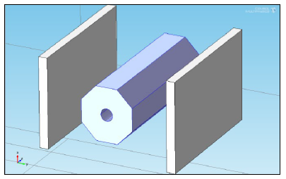
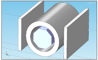
As can be seen in Figure 4, adding a protective ring (Teflon) around the crystal can improve the signal or even the propagation of the electromagnetic wave throughout the crystal. This is the principle of channeling. This ring being made of Teflon, it blocks the distribution of the electric field induced by the electrodes within the crystal. It is possible to remedy this problem by using a perforated sheath on the surfaces. This would improve the signal without removing the effect of the electrodes.
Figure 4. Adding a sheath for the optical sensor.
4.2.4. Fourth Configuration
Figure 5 shows a stack of lithium niobate crystals. The idea is to scan a set of wavelengths since each crystal is oriented, with respect to the two electrodes, differently from the other crystals. In this configuration, several factors have to be taken into consideration, in particular the influence of the electric field on each crystal which will cause, due to the interaction between neighboring crystals, a disturbance of the electric field within this same crystal.
Figure 5. Stacking of crystals
5.1 Study of the response of a wave guide
We make a waveguide designed from Lithium Niobate. This guide is, then, put in the air; it is excited with an electromagnetic wave. We can see that the wave propagates throughout the guide as shown in Figure 6.
Figure 6. Propagation of an EM wave in a waveguide
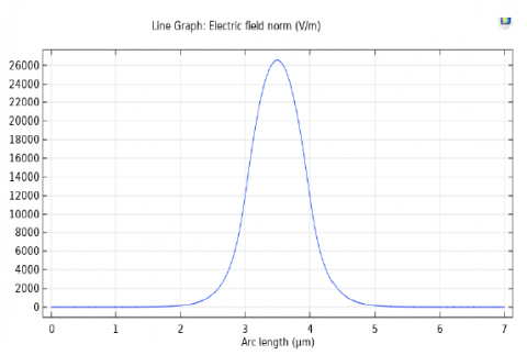
Figure 7. Measuring the electric field inside the guide
The frequency of the wave used is 193.41 THz, with an ambient temperature of 25 °C, a guide’s length of 10 μm and a thickness of 1 μm. We will try to measure the electric field inside the guide using a perfect electric conductor (capacity principle). The result is shown in Figure 7.
It can be seen that the electric field is maximum at the heart of the guide. The further away from the heart, the more the amplitude of the field decreases to cancel itself out of the guide.
The wave propagation in the guide is characterized by the value of the ordinary refractive index of this one, expressed by the following Sellmeier equation:
$\sqrt{\begin{array}{l}4.9048+ \\ \frac{117750+0.022314(T-24.5)(T+570.5)}{\lambda^{2}-(218.02-} \\ 0.000029671(T-24.5)(T+570.5))^{2} \\ +0.000000021429(T-24.5)(T+570.5) \\ -0.000000027153 \lambda^{2}\end{array}}$ (11)
We note that this refractive index depends on two essential parameters, which are the temperature $\mathrm{T}\left({ }^{\circ} \mathrm{C}\right)$ and the wavelength $\lambda$ (nm).
The goal of our work is focused on controlling the response of the electric field under the effect of temperature and the influence of the guide’s length.
5.1.1 The effect of Temperature on the Electric Field
By varying the temperature, the refractive index is changed and the electric field is disturbed inside the waveguide. This is illustrated in Figure 8. The propagation being disturbed, this will have an influence on the electric field.
Figure 8. EM wave propagation for different temperature values
We notice in Figure 9 that, the higher the temperature, the lower the electric field.
Figure 9. Measurement of the electric field for different temperature values
5.1.2 Influence of the Waveguide’s Length
In addition to the 10 μm length guide, we will test the wave propagation in a smaller guide (5 μm). We obtain the following Figures 10 and 11.
Figure 10. Response of a 10 μm length guide
Note that the longer the guide is, the more attenuated the signal is throughout it. For the same excitation source, the two guides react differently to their two respective inputs: the photons of the EM wave are more condensed for the short guide, and therefore, are more concentrated.
Figure 11. Response of a 5 μm length guide
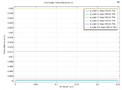
By measuring the transmittance and reflectance of several guides of different lengths, the following results are obtained (Figures 12 and 13).
Figure 12. Transmittance of guides of different lengths
The shorter the guide is, the more we have an almost total transmittance and an almost zero reflectance; and vice versa.
Figure 13. Reflectance of guides of different lengths
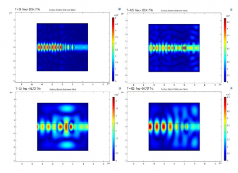
5.1.3 Inserting a Bragg Grating in A Waveguide
The Bragg period $\Lambda$ being calculated according to the formula $\lambda=2 . n . \Lambda(\lambda$ being the wavelength, $\mathrm{n}$ the refractive index $n_{0}$ ). We will install this grating (network) on 4 guides and we will obtain the following results (Figure 14):
Figure 14. Wave behavior in the presence of a Bragg grating
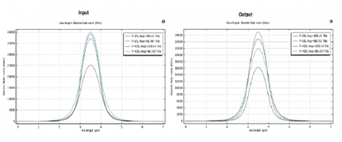
Figure 15. Influence of the Bragg grating on the signal input, and on its output
For an electromagnetic wave of frequency 193.41 THz, wavelength 1550 nm and at 25 °C, the Bragg grating blocks the wave and, at the output, a weak signal compared to the input is recovered.
This same grating no longer operates correctly by varying the value of the temperature or that of the wavelength. These latter directly influence the refractive index n, which will cause a change in the value of the Bragg period $\Lambda$[22].
In conclusion, we can say that a Bragg grating is specific to wavelength and temperature. This can be confirmed from the expression of the Bragg period $\Lambda=\lambda /(2 . n)$.
By measuring the electric field, the following results are obtained (Figure 15.)
We also note that the network does not act only at the output of the guide but also at its input. This allows us to explain the attenuation of each wave in relation to the frequency emitted.
5.2 Study of the Response of Several Waveguides
As shown in Figure 16, three waveguides are excited with an electromagnetic source. The 1 μm separates the three guides.
Figure 16. Excitation of the 3 guides
The electric field is measured at the output of each guide. We obtain the following curves (Figure 17).
Figure 17. Measurement of the electric field
When several guides are assembled, the light behaves differently. The wave guiding of the central guide is influenced by the presence of the other two guides. The electric field is stronger in the central guide.
However, the signal intensity and electric field values remain less important than when the guide was excited on its own.
5.2.1 Variation in Length of the Guides
The temperature value will be set at 25 °C and the wave frequency at 193.41 THz. We will take guides whit lengths equal to 5um, 7.5um, 10um.
We see that whatever the length of the guides, the EM wave is confined and the electric field is almost the same (the signals are confused) whether in the main guide or in the two others (Figure 18).
Figure 18. Influence of guide’s length on signal response
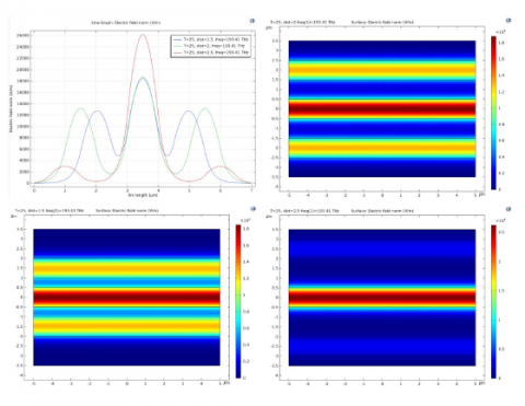
5.2.2 Variation of the Distance Between the Guides
For guides whit length 10um and at temperature of 25 °C, the distance between the guides will be 1.5um, 2um, and 2.5um.
Figure 19. Impact of the distance between the guides on the signal propagation
We can see in Figure 19, the greater the distance, the more important the signal is in the central guide and gets lost in the other two, and the higher the electric field is at the heart of the central guide.
5.2.3 Variation of Temperature
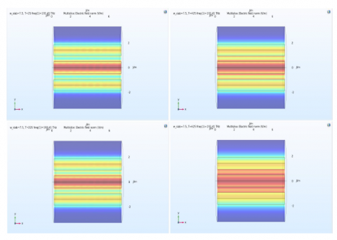
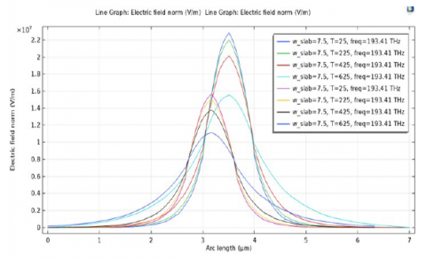
After having found that the length of the guide has almost no influence on the electric field, we will take for example a length of 7.5um for the guides and a distance of 0.5um separating them.
Central guide surrounded by two guides:
The temperature will vary from 25 ° C to 625 ° C with a stepa 200 ° C pitch.
We see in the Figure 20 that the higher the temperature, the weaker the containment phenomenon and the more refracted the wave. This leads to a phenomenon of dispersion.
The electric field is measured in the central guide and one of the other two guides at the end of the device. The following results are obtained:
Figure 20. Impact of temperature on wave propagation in the guides
Figure 21. Measuring the electric field in the central guide and in one of the two remaining guides
As can be seen in the Figure 21, the increase in the temperature value leads to the decrease in the value of the electric field whether in the central guide or at the end.
Central guide surrounded with multiple guides:
A device consisting of 9 guides with a length of 10 μm willbe excited with an EM wave, as illustrated in the Figure 22.
Figure 22. Device with 9 waveguides
The electric field is measured for different temperature values.
The luminous flux is more intense at the center relative to the ends; therefore, the electric field is stronger at the center.
It can be seen in the Figure 23 that the higher the temperature, the lower the electric field. Also, this field is disturbed, whether in the center or in the ends.
Figure 23. Variation of the electric field as a function of temperature
Currently, optical technology plays an important role in thefield of nanotechnology. The increasing control of the production of optical components now makes it possible to produce easy-to-use, accurate and stable sensors. This research focused on the theoretical study of an optical sensor based on the electro-optical effect induced by lithium niobate.
A method for producing an optoelectronic sensor was then proposed. Our study focused on the physical phenomenon of detecting an electromagnetic wave; several radiometric quantities were identified.
In addition to these quantities and the electromagnetic wave, other factors are involved in manufacturing the sensor. In this context, it was decided to study the electro-optical (E/O) effect or the Pockels effect induced by the birefringent anisotropic materials, which aroused the interest of choosing the lithium niobate crystal whose properties are revealed to be fascinating, at the nanometric scale.
The Authors extend their thanks to the Deanship of Scientific Research at King Khalid University for funding this work through the big research groups under grant number RGP. 1/155/42.
This research work was supported by the Deanship of Scientific Research at King Khalid University under Grant number RGP. 1/155/42.
[1] Ha, N.B. (2011). Introductory nanoscience: physical andchemical concepts. Advances in Natural Sciences:Nanoscience and Nanotechnology, 2(4): 049301.https://doi.org/10.1088/2043-6254/2/4/049301
[2] Ferreira, M.F., Castro-Camus, E., Ottaway, D.J., López-Higuera, J.M., Feng, X., Jin, W., Quan, Q. (2017). Roadmap on optical sensors. Journal of Optics, 19(8): 083001. https://doi.org/10.1088/2040-8986/aa7419
[3] Takahashi, T.T.T., Hidaka, K.H.K., Kouno, T.K.T.(1996). New optical-waveguide pockels sensor formeasuring electric fields. Japanese Journal of AppliedPhysics, 35(2R): 767.https://doi.org/10.1143/JJAP.35.767
[4] Hamze, A.K., Reynaud, M., Geler-Kremer, J., Demkov,A.A. (2020). Design rules for strong electro-opticmaterials. NPJ Computational Materials, 6(1): 1-9.https://doi.org/10.1038/s41524-020-00399-z
[5] Brunetti, M.N., Berman, O.L., Kezerashvili, R.Y.(2019). Optical properties of anisotropic excitons inphosphorene. Physical Review B, 100(15): 155433.https://doi.org/10.1103/PhysRevB.100.155433
[6] Wu, S.T., Efron, U., Hess, L.D. (1984). Birefringencemeasurements of liquid crystals. Applied Optics, 23(21):3911-3915. https://doi.org/10.1364/AO.23.003911
[7] Mathieu, H., Fanet, H. (2009). Physique dessemiconducteurs et des composants électroniques-6èmeédition: Cours et exercices corrigés. Dunod. 6e édition.
[8] Birman, M.S., Solomyak, M.Z. (1987). L2-theory of theMaxwell operator in arbitrary domains. RussianMathematical Surveys, 42(6): 75.
[9] Han, S.E. (2020). Transport mean free path tensor andanisotropy tensor in anisotropic diffusion equation foroptical media. Journal of Optics, 22(7): 075606.https://doi.org/10.1088/2040-8986/ab954d
[10] Stadnyk, V.I., Kushnir, O.S., Brezvin, R.S., Gaba, V.M.(2009). Temperature and baric changes in the refractiveindices of LiKSO4 crystals. Optics and Spectroscopy,106(4): 614-620.https://doi.org/10.1134/S0030400X09040237
[11] Treussart, F. (2008). Cours d’optique anisotrope.Préparation à l'Agrégation de Sciences Physiques (ENSCachan). http://old.physique-ens-cachan.educ.space/pagregp/cours/fichiers/Cours_opt_anis_v2_5.pdf
[12] Shirouzu, S., Shigematsu, K., Sakamoto, S., Nakagawa,T., Tagami, S. (1989). Refractive index ellipsoids of apolycarbonate magneto optical memory disk substrate.Japanese Journal of Applied Physics, 28(5): 797-800.https://doi.org/10.1143/JJAP.28.797
[13] Kawanishi, T., Ogura, H., Wang, Z.L. (1997).Polarization characteristics of an electromagnetic wavescattered from a slightly random surface: polarizedincidence. Waves in Random Media, 7(4): 593.https://doi.org/10.1088/0959-7174/7/4/006
[14] Parfitt, H.T., Robertson, D.S. (1967). Domain structuresin lithium niobate crystals. British Journal of AppliedPhysics, 18(12): 1709. https://doi.org/10.1088/0508-3443/18/12/305
[15] Grousson, R. (1982). Propriétés photoréfractives duniobate de lithium et leurs applications au traitementd'image. Doctoral dissertation, Université Pierre et MarieCurie-Paris VI.
[16] Chen, L., Xu, Q., Wood, M.G., Reano, R.M. (2014).Hybrid silicon and lithium niobate electro-optical ringmodulator. Optica, 1(2): 112-118.https://doi.org/10.1364/OPTICA.1.000112
[17] Wessels, B.W. (2007). Ferroelectric epitaxial thin filmsfor integrated optics. Annual Review of MaterialsResearch, 37: 659-679.https://doi.org/10.1146/annurev.matsci.37.052506.084226
[18] Weller, E.F. (1967). Lithium niobate-a new type offerroelectrics: growth, structure and properties. ElsevierPub. Co.
[19] Wang, C., Zhang, M., Stern, B., Lipson, M., Lončar, M.(2018). Nanophotonic lithium niobate electro-opticmodulators. Optics Express, 26(2): 1547-1555.https://doi.org/10.1364/OE.26.001547
[20] Jazbinšek, M.O.J.C.A., Zgonik, M. (2002). Materialtensor parameters of LiNbO3 relevant for electro-and elasto-optics. Applied Physics B, 74(4): 407-414. https://doi.org/10.1007/s003400200818
[21] Tian, K., Liu, Y., Wang, Q. (2005). Temperature-independent fiber Bragg grating strain sensor usingbimetal cantilever. Optical Fiber Technology, 11(4):370-377. https://doi.org/10.1016/j.yofte.2005.03.001
[22] Zhang, D., Wang, J., Wang, Y., Dai, X. (2014). A fastresponse temperature sensor based on fiber Bragggrating. Measurement Science and Technology, 25(7):075105. https://doi.org/10.1088/0957-0233/25/7/075105