M. R. D. Al-Mothafar
© 2022 IIETA. This article is published by IIETA and is licensed under the CC BY 4.0 license (http://creativecommons.org/licenses/by/4.0/).
OPEN ACCESS
This work studies the small-signal direct and cross-coupling audio-susceptibilities of the independent-input series-output boost converter with peak current-mode control. The converter functions in the continuous-conduction mode and comprises n-connected identical boost modules whose inputs are fed from separate voltage sources and outputs connected in series. Expressions for the module direct (self) and cross-coupling audio-susceptibilities are derived in symbolic form. The expressions explicitly show (n) as a variable and take into account the sampling action of the current loops. In addition, audio-susceptibilty frequency responses following the closure of the voltage feedback loops are generated and the influence of increasing n is discussed. Detailed simulations using PSIM are performed to support the analysis.
audio-susceptibility, modular boost dc-dc converters, independent-input series-output, peak current-mode control, small-signal modeling
Over the past few decades, the modular connection of dc-dc converters has shown effectiveness in reducing current and voltage stresses on the participating semiconductor devices and also in increasing the conversion system reliability. A modular converter allows power to be processed by a number of converter modules connected in different combinations to fulfil certain input/output requirements. The four well-known conventional arrangements of modular converters are: the parallel-input/parallel-output (PIPO), the parallel-input/series-output (PISO), the series-input/parallel-output (SIPO), and the series-input/series-output (SISO); the works [1, 2] are comprehensive references on the subject. Other arrangements, however, have appeared in the literature like the series-parallel-input/series-output [3], the series-input/series-parallel-output [4], and the independent-input arrangements, namely the independent-input/series-output (IISO) [5-15], and the independent-input/parallel-output (IIPO) [16-19].
Several control methodologies have been proposed for these modular converters, among them is the peak current-mode control (PCMC) technique due to its renowned merits such as fast response, stable current sharing and precise output voltage regulation [1]. PCMC has been used for the control of PIPO [20-23], PISO [24-26], SIPO [27-29], SISO [30, 31], IISO [14], and IIPO [16] converters. Initial examination of the dynamics of these systems is dominantly done with the help of linearised small-signal (SS) models. Better insight into the converter performance can be obtained if SS modeling is supported by transfer function expressions showing how the system behaves as the number of modules is varied.
The SS line-to-output voltage transfer function (audio-susceptibility) of a dc-dc converter cell is an important dynamic performance parameter. It describes the converter’s ability to attenuate SS input voltage disturbances. The audio- susceptibilities of several PCMC single-stage dc-dc converters have been formally studied [32-36]. Also many papers addressed the audio-susceptibilities of the conventional PCMC single-input modular converters [20, 24, 26, 28]. Nevertheless, susceptibilities of PCMC modular converters supplied from n-independent sources and how these susceptibilities react to varying the number of modules under open and closed-loop conditions have never been treated in the literature. In such converters like the IISO and the IIPO there are two audio-susceptibilities to consider: 1) The direct (self) audio-susceptibility which defines the output voltage response of a certain module due to a disturbance in its input voltage; and 2) the cross-coupling audio- susceptibility which gives the output voltage response of one module due to a disturbance in the source voltage of another.
The objective of this work is to study analytically the SS direct and cross-coupling audio-susceptibilities of an IISO PCMC boost converter intended for dc power supplies applications. Converters using the IISO structure have the distinct feature of being supplied from independent voltage sources; with higher output voltages obtained by the series connection of the outputs of a number of single-cell converters. The pioneer work on IISO dc-dc converters dates back to the 1990’s [5] where a two module IISO boost configuration was used to interface a small-size wind-photovoltaic system to the utility circuit. Since then many articles have been written on IISO converters for different applications related to renewable energy systems, distributed power systems and dedicated dc power supplies, but none of them have employed PCMC for the control of the constituent modules until recently [14] where the ramp-compensated PCMC is used to control an IISO boost converter. The work [14], however, has only focused on the control-to-output voltage SS responses produced numerically using Simulink software. Other performance parameters like audio-susceptibility and cross-coupling effect have not been considered.
The contributions of this paper are: 1) the SS direct and cross-coupling audio-susceptibilities of the PCMC IISO boost converter are analytically studied. Symbolic expressions for these transfers are derived after establishing a small-signal model based on state-space equations. The expressions explicitly show the number of used cells (n) and take into account the sampling action of each of the converter’s current loops. These expressions help the user to readily plot SS responses for different n without needing a circuit simulator; 2) the study also addresses the effect of closing the voltage feedback loops on the audio-susceptibilities when classical controllers are employed. To validate the analysis, two, three, and four-module converters are implemented using PSIM and frequency responses are obtained using the “ac sweep” tool which allows the user to obtain the frequency response while the converter is in its switched-mode form.
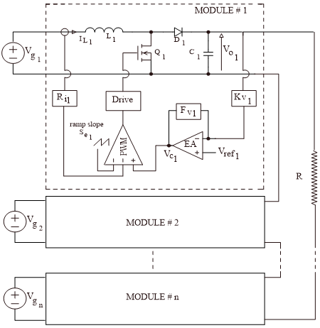
The IISO converter considered in this study is depicted in Figure 1. Several identical PCMC boost modules are operated in the continuous-current conduction mode and joined in series at the output side to supply a common load. A separate voltage source feeds each of the independently controlled modules. The PCMC of each module in Figure 1 can be briefly reviewed as follows: Converter switching cycle is started by a constant-frequency clock. Transistor’s duty ratio (D) is set when the inductor current, after being sensed by (Ri), becomes equal to a value that depends on control voltage (Vc), produced by the compensated error amplifier (EA) circuit, and an external ramp slope (Se). This ramp is necessary to stabilize the current loop if D is greater than 0.5 [32]. Also in Figure 1, the attenuation factor of the module output voltage is denoted by Kv while Fv represents the module voltage-loop compensator transfer function.
The following sections of this paper are: Section 2 presents the converter SS model. Section 3 studies the direct and cross-coupling audio-susceptibilities with closed current loops and voltage loops left open. Section 4 addresses the effect of closing the voltage feedback loops on the audio-susceptibilities. Finally, Section 5 contains the conclusion.
Figure 1. IISO converter schematic
2.1 Modeling the power stage
To develop the SS model of the multi-module PCMC converter, a two module converter is considered first. Referring to Figure 1, the input and output voltages of each module is denoted by Vg and Vo respectively; the module inductor current is indicated by IL, and the transistor duty ratio of each module is symbolised by D. Using state-space averaging and linearization [37], the power-stage SS model of a two-module IISO boost converter assuming ideal components can be characterized as in Ref. [14] by:
$\dot{\hat{x}}=\frac{d}{d t}\left[\begin{array}{c}\hat{\imath}_{L 1} \\ \hat{v}_{o 1} \\ \hat{\imath}_{L 2} \\ \hat{v}_{o 2}\end{array}\right]=[A]\left[\begin{array}{c}\hat{\imath}_{L 1} \\ \hat{v}_{o 1} \\ \hat{\imath}_{L 2} \\ \hat{v}_{o 2}\end{array}\right]+[B]\left[\begin{array}{c}\hat{d}_1 \\ \hat{d}_2 \\ \hat{v}_{g 1} \\ \hat{v}_{g 2} \\ \hat{\imath}_o\end{array}\right]$ (1a)
where
$[A]=\left[\begin{array}{cccc}0 & \frac{-D_1^{\prime}}{L_1} & 0 & 0 \\ \frac{D_1^{\prime}}{C_1} & \frac{-1}{R C_1} & 0 & \frac{-1}{R C_1} \\ 0 & 0 & 0 & \frac{-D_2^{\prime}}{L_2} \\ 0 & \frac{-1}{R C_2} & \frac{D_2^{\prime}}{C_2} & \frac{-1}{R C_2}\end{array}\right]$ (1b)
$[B]=\left[\begin{array}{ccccc}\frac{V_{g 1}}{D_1^{\prime} L_1} & 0 & \frac{1}{L_1} & 0 & 0 \\ \frac{-2 V_{g 1}}{D_1^{\prime 2} R C_1} & 0 & 0 & 0 & \frac{1}{C_1} \\ 0 & \frac{V_{g 2}}{D_2^{\prime} L_2} & 0 & \frac{1}{L_2} & 0 \\ 0 & \frac{-2 V_{g 2}}{D_2^{\prime 2} R C_2} & 0 & 0 & \frac{1}{C_2}\end{array}\right]$ (1c)
where the hat symbol (^) is used for SS changes; and $D^{\prime}=1-D$.
2.2 Modeling the PCMC stage
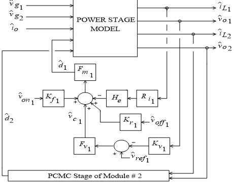
The PCMC stage of each module is modeled in a similar fashion to that of the single boost dc-dc converter [32, 33]. The SS model for a 2-module converter is illustrated in Figure 2(a). Each module is comprised of: The current sensing resistance Ri; the PWM modulator gain Fm; the current loop sampling gain He; and feedforward gains Kfand Krformed as a result of closing the current loop of each module. Variations in the inductor voltage during the ON and OFF intervals of the transistor are respectively denoted as $\hat{v}_{o n}$ and $\hat{v}_{o f f}$. Model parameters are given in Table 1. The module duty ratio with only the current loop closed is:
$\hat{d}=F_m\left(\hat{v}_c-R_i H_e \hat{\imath}_L+K_f \hat{v}_{o n}+K_r \hat{v}_{o f f}\right)$ (2)
After the application of Laplace transforms to (1) and the substitution for duty ratio ($\hat{d}$) from (2), we get the following when the modules are identical:
$\left[\begin{array}{c}s \hat{v}_{L 1} \\ s \hat{v}_{o 1} \\ s \hat{l}_{L 2} \\ s \hat{v}_{o 2}\end{array}\right]=\left[\begin{array}{cccc}A_1 & A_2 & 0 & 0 \\ A_3 & A_4 & 0 & A_5 \\ 0 & 0 & A_1 & A_2 \\ 0 & A_5 & A_3 & A_4\end{array}\right]\left[\begin{array}{c}\hat{l}_{L 1} \\ \hat{v}_{o 1} \\ \hat{l}_{L 2} \\ \hat{v}_{o 2}\end{array}\right]+\left[\begin{array}{ccccc}B_1 & 0 & B_2 & 0 & 0 \\ B_3 & 0 & B_4 & 0 & B_5 \\ 0 & B_1 & 0 & B_2 & 0 \\ 0 & B_3 & 0 & B_4 & B_5\end{array}\right]\left[\begin{array}{c}\hat{v}_{c 1} \\ \hat{v}_{c 2} \\ \hat{v}_{g 1} \\ \hat{v}_{g 2} \\ \hat{\imath}_o\end{array}\right]$ (3)
The A and B elements are tabulated in Table 2, and parameters Fm, He, Kr and Kf are as given in Table 1.
The set of Eq. (3) represents the converter SS model with only the current loops closed.
(a) Block diagram
(b) Structure of Type II compensator
Figure 2. Two-module small-signal model
Table 1. Parameters of figure 2(a)
|
$F_m=\frac{1}{\left(S_n+S_e\right) T}=\frac{L}{M_c R_i V_g T} \quad \text { where } M_c=1+s_e / s_n |
|
$H_e \cong\left(1+\frac{s}{\omega_n Q_z}+\frac{s^2}{\omega_n^2}\right)$ where $Q_z=-2 / \pi$ and $\omega_n=\pi / T$ |
|
$K_f=-\frac{D T R_i(1-0.5 D)}{L}+\frac{D^2 T^2 R_i(3-2 D)}{12 L} s$ and $K_r=\frac{D^{\prime 2} T R_i}{2 L}$ |
|
$\hat{v}_{\text {on }}=\hat{v}_g ; \hat{v}_{\text {off }}=\hat{v}_o-\hat{v}_g$ |
|
$F_v=\frac{k_i\left(1+s / \omega_z\right)}{s\left(1+s / \omega_p\right)}$ |
Table 2. Summary of the expressions of Eq. (3)
|
A1 |
$\frac{-V_{o, \text { module }}\,\,\,\,\,\, R_i H_e F_m}{L}$ |
B1 |
$\frac{V_{o, \text { module }}\,\,\,\,\,\, F_m}{L}$ |
|
A2 |
$\frac{-D^{\prime}+V_{o, \text { module }}\,\,\,\,\,\, F_m K_r}{L}$ |
B2 |
$\frac{1+V_{o, \text { module }}\,\,\,\,\,\, F_m\left(K_f-K_r\right)}{L}$ |
|
A3 |
$\frac{D^{\prime}+I_{L, \text { module }}\,\,\,\,\,\, R_i H_e F_m}{C}$ |
B3 |
$\frac{-I_{L, \text { module }}\,\,\,\,\,\, F_m}{C}$ |
|
A4 |
$\frac{-1}{C}\left(\frac{1}{R}+I_{L, \text { module }} F_m K_r\right)$ |
B4 |
$\frac{-I_{L, \text { module }}\,\,\,\,\,\, F_m\left(K_f-K_r\right)}{C}$ |
|
A5 |
$\frac{-1}{R C}$ |
B5 |
$\frac{1}{C}$ |
2.3 Modeling the voltage feedback loop stage
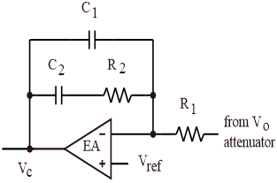
Referring to Figure 2(a), the voltage feedback loop of each module consists of an attenuator Kv and a classical (type II) compensator represented by Fv. The compensator structure is depicted in Figure 2(b). With voltage and current feedback loops closed, Eq. (3) is updated by substituting for the control voltages vC1 and vC2 which can be expressed as:
$\hat{v}_{c 1}=\left(\hat{v}_{\text {ref } 1}-K_{v 1} \hat{v}_{o 1}\right) F_{v 1}$ (4a)
$\hat{v}_{c 2}=\left(\hat{v}_{r e f 2}-K_{v 2} \hat{v}_{o 2}\right) F_{v 2}$ (4b)
The SS model for the 2-module converter is represented as:
$\left[\begin{array}{c}s \hat{l}_{L 1} \\ s \hat{v}_{o 1} \\ s \hat{\imath}_{L 2} \\ s \hat{v}_{o 2}\end{array}\right]=\left[\begin{array}{cccc}A_1 & A_2-B_1 K_{v 1} F_{v 1} & 0 & 0 \\ A_3 & A_4-B_3 K_{v 1} F_{v 1} & 0 & A_5 \\ 0 & 0 & A_1 & A_2-B_1 K_{v 2} F_{v 2} \\ 0 & A_5 & A_3 & A_4-B_3 K_{v 2} F_{v 2}\end{array}\right]\left[\begin{array}{c}\hat{\imath}_{L 1} \\ \hat{v}_{o 1} \\ \hat{l}_{L 2} \\ \hat{v}_{o 2}\end{array}\right]+\left[\begin{array}{ccccc}B_1 F_{v 1} & 0 & B_2 & 0 & 0 \\ B_3 F_{v 1} & 0 & B_4 & 0 & B_5 \\ 0 & B_1 F_{v 2} & 0 & B_2 & 0 \\ 0 & B_3 F_{v 2} & 0 & B_4 & B_5\end{array}\right]\left[\begin{array}{c}\hat{v}_{r e f 1} \\ \hat{v}_{r e f 2} \\ \hat{v}_{g 1} \\ \hat{v}_{g 2} \\ \hat{l}_o\end{array}\right]$ (5)
3.1 Module direct audio-susceptibility
The direct (self) audio-susceptibility of a certain module is the output voltage response of that module due to a disturbance in its input voltage. The case of a two-module converter (n = 2) will be used as a starting point to reach a general SS expression for the audio-susceptibilities with n-connected modules. Referring to (3), the module direct audio-susceptibility when n = 2 can be expressed as:
$\frac{\hat{v}_{o 1}}{\hat{v}_{g 1}}=\frac{\hat{v}_{o 2}}{\hat{v}_{g 2}}=\frac{\Delta_1\left[s^2-\left(A_1+A_4\right) s+A_1 A_4-A_2 A_3\right]}{\Delta_2\left[s^2-\left(A_1+A_4+A_5\right) s+A_1\left(A_4+A_5\right)-A_2 A_3\right]}$ (6)
$\Delta_1=B_4\left(s-A_1+A_3 B_2 / B_4\right)$ (7a)
$\Delta_2=s^2-\left(A_1+A_4-A_5\right) s+A_1\left(A_4-A_5\right)-A_2 A_3$ (7b)
A general expression for the direct audio-susceptibility of a converter with n-connected modules can be concluded when we find the susceptibilities of the three and four-module converters which can be reached by following the steps used above with the two-module case.
When n = 3, the direct audio-susceptibility can be derived as:
$\frac{\hat{v}_{o 1}}{\hat{v}_{g 1}}=\frac{\hat{v}_{o 2}}{\hat{v}_{g 2}}=\frac{\hat{v}_{o 3}}{\hat{v}_{g 3}}=\frac{\Delta_1\left[s^2-\left(A_1+A_4+A_5\right) s+A_1\left(A_4+A_5\right)-A_2 A_3\right]}{\Delta_2\left[s^2-\left(A_1+A_4+2 A_5\right) s+A_1\left(A_4+2 A_5\right)-A_2 A_3\right]}$ (8)
And for n = 4
$\frac{\hat{v}_{o 1}}{\hat{v}_{g 1}}=\frac{\hat{v}_{o 2}}{\hat{v}_{g 2}}=\frac{\hat{v}_{o 3}}{\hat{v}_{g 3}}=\frac{\hat{v}_{o 4}}{\hat{v}_{g 4}}=\frac{\Delta_1\left[s^2-\left(A_1+A_4+2 A_5\right) s+A_1\left(A_4+2 A_5\right)-A_2 A_3\right]}{\Delta_2\left[s^2-\left(A_1+A_4+3 A_5\right) s+A_1\left(A_4+3 A_5\right)-A_2 A_3\right]}$ (9)
In general, for the n-connected modules shown in Figure 1, the module direct audio-susceptibilty is:
$\frac{\hat{v}_{\text {on }}}{\hat{v}_{g n}}=\frac{\Delta_1}{\Delta_2} \times \frac{\left[s^2-\left(A_1+A_4+(n-2) A_5\right) s+A_1\left(A_4+(n-2) A_5\right)-A_2 A_3\right]}{\left[s^2-\left(A_1+A_4+(n-1) A_5\right) s+A_1\left(A_4+(n-1) A_5\right)-A_2 A_3\right]}$ (10)
The expression is 5th order for the numerator and 6th for the denominator when we substitute for the A and B terms given in Table 2. After performing these substitutions and rearranging terms the resultant expression is programmed into Matlab with the following parameters for each module:
Vg = (48/number of modules) V; D = 0.6; R = 30 Ω;
T = 10 µs; L = 115 µH; C = 40 µF; Ri = 0.1 Ω
The direct audio-susceptibility can be evaluated for different slope ratio (Mc) values by using Eq. (10).
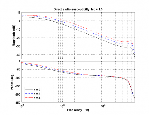
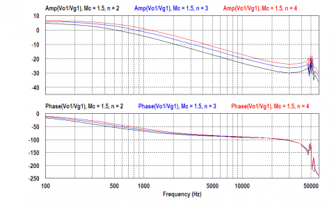
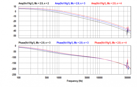
Figure 3 shows the direct audio-susceptibility responses as we vary n with slope ratio Mc= 1.5 while Figure 4 depicts the responses when Mc = 2.9. The slope-ratio values are selected to study the underdamped and critically-damped behaviour. Figures 3 and 4 also present PSIM “ac sweep” results to validate the analytical model predictions. Matlab pole-zero locations corresponding to these cases are given in Table 3. In the module audio-susceptibility response, at low frequencies, one can notice that there are two real left-half s-plane poles sandwiching a real zero. At ½ the switching frequency (fs/2), the response is influenced by a complex pair of poles in the left-half plane as a result of the sample-and-hold (S/H) effect of PCMC, and hence the peaking in Figure 3 when Mc = 1.5. This double pole however splits up into two single real poles with Mc = 2.9. The S/H effect also creates a complex pair of left-half-plane zeros in the module audio-susceptibility response at frequencies higher than fs/2. Figures 3 and 4 show that increasing the number of modules increases the direct audio-susceptibility, but does not have a noticeable effect on the peaking at fs/2; and critical damping of the responses is achieved for all cases with the same slope ratio.
(a) Plots from analytical model
(b) PSIM simulation results
Figure 3. Direct audio-susceptibility with current loops closed and variable number of modules with (Mc = 1.5)
(a) Plots from analytical model
(b) PSIM simulation results
Figure 4. Direct audio-susceptibility with current loops closed and variable number of modules with (Mc = 2.9)
Table 3. Pole-zero locations in (rad/sec) of direct audio-susceptibility with variable n
|
|
MC = 1.5 |
MC = 2.9 |
||||
|
|
n = 2 |
n = 3 |
n = 4 |
n = 2 |
n = 3 |
n = 4 |
|
Zeros |
1.0e+05 * -0.1189 + 4.6336i -0.1189 - 4.6336i -0.3940 + 3.1066i -0.3940 - 3.1066i -0.0265 + 0.0000i |
1.0e+05 * -0.0792 + 4.6218i -0.0792 - 4.6218i -0.3940 + 3.1015i -0.3940 - 3.1015i -0.0350 + 0.0000i |
1.0e+05 * -0.0594 + 4.6157i -0.0594 - 4.6157i -0.3938 + 3.0965i -0.3938 - 3.0965i -0.0435 + 0.0000i |
1.0e+05 * -0.1189 + 4.8924i -0.1189 - 4.8924i -3.6775 + 0.0000i -2.6353 + 0.0000i -0.0288 + 0.0000i |
1.0e+05 * -0.0792 + 4.7963i -0.0792 - 4.7963i -3.7480 + 0.0000i -2.5643 + 0.0000i -0.0376 + 0.0000i |
1.0e+05 * -0.0594 + 4.7474i -0.0594 - 4.7474i -3.8112 + 0.0000i -2.5005 + 0.0000i -0.0465 + 0.0000i |
|
Poles |
1.0e+05 * -0.3941 + 3.1066i -0.3941 - 3.1066i -0.3940 + 3.1066i -0.3940 - 3.1066i -0.0349 + 0.0000i -0.0181 + 0.0000i |
1.0e+05 * -0.3940 + 3.1015i -0.3940 - 3.1015i -0.3939 + 3.1015i -0.3939 - 3.1015i -0.0434 + 0.0000i -0.0266 + 0.0000i |
1.0e+05 * -0.3939 + 3.0965i -0.3939 - 3.0965i -0.3938 + 3.0965i -0.3938 - 3.0965i -0.0520 + 0.0000i -0.0351 + 0.0000i |
1.0e+05 * -3.6779 -3.6771 -2.6358 -2.6348 -0.0373 -0.0203 |
1.0e+05 * -3.7485 -3.7475 -2.5650 -2.5636 -0.0461 -0.0290 |
1.0e+05 * -3.8117 -3.8106 -2.5013 -2.4996 -0.0552 -0.0379 |
3.2 Module cross-coupling audio-susceptibility
The cross-coupling audio-susceptibility is the output voltage response of one module due to a disturbance in the source voltage of another. Following the same procedure used above for deriving the direct audio-susceptibilty, the cross-coupling audio susceptibility can be derived as:
$\left(\frac{\hat{v}_{o n}}{\hat{v}_{g n}}\right)_{\text {cross }}=\frac{\Delta_1}{\Delta_2} \times \frac{A_5\left(s-A_1\right)}{\left[s^2-\left(A_1+A_4+(n-1) A_5\right) s+A_1\left(A_4+(n-1) A_5\right)-A_2 A_3\right]}$ (11)
where, Δ1 and Δ2 are as given by Eq. (7); and A1-to-A5 are defined in Table 2.
(a) Plots from analytical model
(b) PSIM simulation results
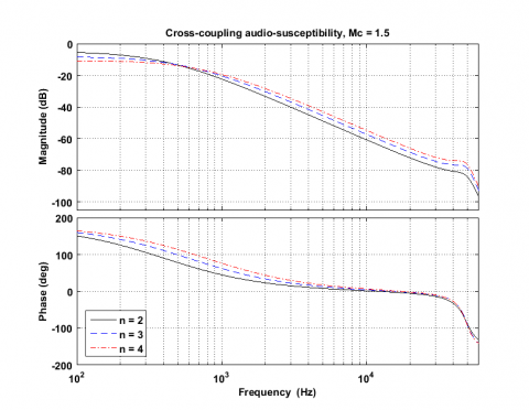
Figure 5. Cross-coupling audio-susceptibility with current loops closed and variable number of modules (Mc = 1.5)
Figure 5 shows the predicted cross-coupling audio-susceptibility responses as we vary n with slope ratio Mc= 1.5 while Figure 6 depicts the responses when Mc = 2.9. Corresponding Matlab pole-zero locations appear in Table 4; the denominator of this transfer function is of course the same as that of the direct audio-susceptibility, but the numerator is one order lower. From Figures 5 and 6, it can be noticed that: 1) the cross-coupling audio-susceptibility is less than the direct audio-susceptibility; 2) At low frequencies the audio-susceptibility is reduced with the addition of modules, but as perturbation frequency rises, the susceptibility will increase when modules are added.
(a) Plots from analytical model
(b) PSIM simulation results
Figure 6. Cross-coupling audio-susceptibility with current loops closed and variable number of modules (Mc = 2.9)
Table 4. Pole-zero locations in (rad/sec) for cross-coupling audio-susceptibilty with variable n
|
|
MC = 1.5 |
MC = 2.9 |
||||
|
|
n = 2 |
n = 3 |
n = 4 |
n = 2 |
n = 3 |
n = 4 |
|
Zeros |
1.0e+05 * -0.1189 + 4.6336i -0.1189 – 4.6336i -0.3948 + 3.1167i -0.3948 – 3.1167i |
1.0e+05 * -0.0792 + 4.6218i -0.0792 – 4.6218i -0.3948 + 3.1167i -0.3948 – 3.1167i |
1.0e+05 * -0.0594 + 4.6157i -0.0594 – 4.6157i -0.3948 + 3.1167i -0.3948 – 3.1167i |
1.0e+05 * -0.1189 + 4.8924i -0.1189 – 4.8924i -3.4824 + 0.0000i -2.8341 + 0.0000i |
1.0e+05 * -0.0792 + 4.7963i -0.0792 – 4.7963i -3.4824 + 0.0000i -2.8341 + 0.0000i |
1.0e+05 * -0.0594 + 4.7474i -0.0594 – 4.7474i -3.4824 + 0.0000i -2.8341 + 0.0000i |
|
Poles |
1.0e+05 * -0.3941 + 3.1066i -0.3941 – 3.1066i -0.3940 + 3.1066i -0.3940 – 3.1066i -0.0349 + 0.0000i -0.0181 + 0.0000i |
1.0e+05 * -0.3940 + 3.1015i -0.3940 – 3.1015i -0.3939 + 3.1015i -0.3939 – 3.1015i -0.0434 + 0.0000i -0.0266 + 0.0000i |
1.0e+05 * -0.3939 + 3.0965i -0.3939 – 3.0965i -0.3938 + 3.0965i -0.3938 – 3.0965i -0.0520 + 0.0000i -0.0351 + 0.0000i |
1.0e+05 * -3.6779 -3.6771 -2.6358 -2.6348 -0.0373 -0.0203 |
1.0e+05 * -3.7485 -3.7475 -2.5650 -2.5636 -0.0461 -0.0290 |
1.0e+05 * -3.8117 -3.8106 -2.5013 -2.4996 -0.0552 -0.0379 |
In order to find the module direct and cross-coupling audio-susceptibilities when the current and voltage feedback loops are closed, the general expressions given by Eqns. (10) and (11) can be used but after updating four terms according to Eq. (5). These terms are A2, A4, B1 and B3 which include the output voltage attenuation factor Kv and the compensated error amplifier transfer function Fv.
Designing the module voltage feedback loop compensator is based on its control-to-output voltage response when no peaking is present (i.e. when Mc = 2.9). The control-to-output voltage transfer function is obtained following the same approach used for deriving the audio-susceptibilities and can be expressed as:
$\frac{\hat{v}_{\text {on }}}{\hat{v}_{c n}}=\frac{\Delta_3}{\Delta_2} \times \frac{\left[s^2-\left(A_1+A_4+(n-2) A_5\right) s+A_1\left(A_4+(n-2) A_5\right)-A_2 A_3\right]}{\left[s^2-\left(A_1+A_4+(n-1) A_5\right) s+A_1\left(A_4+(n-1) A_5\right)-A_2 A_3\right]}$ (12)
where, Δ2 is given by (7b) and
$\Delta_3=B_3\left(s-A_1+A_3 B_1 / B_3\right)$ (13)
where the A and B terms are in Table 2.
The compensator should be designed for the case when n is maximum (i.e. n = 4) to ensure that the system is stable when lower number of modules is employed [14]. Usual compensator design procedure used with single-cell converters [38, 39] can be applied for each module. The chosen voltage-loop crossover frequency and phase margin is 800 Hz and 60° respectively.
(a) Plots from analytical model
(b) PSIM simulation results
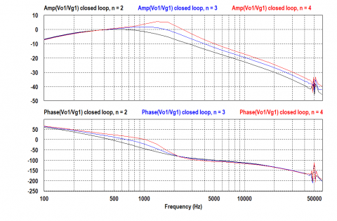
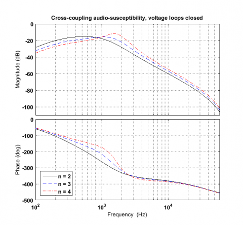
Figure 7. Direct (self) audio-susceptibility with current and voltage feedback loops closed, variable n, and Fv = [6974 (1+s/1919) / s(1+s/13170)]
(a) Plots from analytical model
(b) PSIM simulation results
Figure 8. Cross-coupling audio-susceptibility with current and voltage feedback loops closed, variable n, and Fv = [6974 (1+s/1919) / s(1+s/13170)]
Figures 7 and 8 show the direct and cross-coupling audio-susceptibilities with current and voltage feedback loops closed and variable number of modules. It can be seen that closing the voltage feedback loops benefit the region below the crossover frequency only. Lower audio-susceptibilities can be obtained if the module voltage loop has a higher crossover frequency, but in the IISO boost converter this crossover frequency is limited by the n-dependent right-half-plane zero which appears in the module $\hat{v}_o / \hat{v}_c$ transfer function at the angular frequency $\omega=R(1-D)^2 / n L$.
Figure 7 also shows that increasing n will slightly reduce the direct audio-susceptibility at frequencies below 500 Hz; otherwise, any increase in the number of modules will increase the direct audio-susceptibility. As for the cross-coupling audio-susceptibility, Figure 8 shows that adding modules reduces the susceptibility at frequencies below 900 Hz (by ≈ 7 dB when n is changed from 2 to 4); however, at higher perturbation frequencies this susceptibility increases when modules are added. Due to system’s complexity, the relationship between audio-susceptibilities and the number of modules cannot be quantified by a simple formula, but with a computer program based on the expressions proposed in this work the designer can straightforwardly find the effect of different parameters on the converter audio-susceptibilities.
Symbolic small-signal expressions are presented for both the direct and cross-coupling audio-susceptibilities of the peak current-mode controlled independent-input series-output (IISO) boost dc-dc converter. The derived expressions contain the sample-and-hold effect of the current loops. Using these expressions, the frequency responses under closed current and voltage feedback loop conditions are generated for different number of modules (n). The analytical model results correlate well with the ones obtained from PSIM simulations up to half the switching frequency region.
With the inner (current) and outer (voltage) feedback loops closed, the following can be stated about the module audio-susceptibility: 1) for a certain number of modules the cross-coupling susceptibility is always less than the direct susceptibility; 2) direct susceptibility is slightly reduced when n is increased but only over a small frequency range below the voltage-loop crossover frequency; else, this susceptibility increases with the addition of modules; and 3) cross-coupling susceptibility decreases as n is increased, but only at frequencies below voltage-loop crossover frequency, otherwise, this audio-susceptibility will increase when modules are added.
[1] Luo, S., Ye, Z., Lin, R.L., Lee, F.C. (1999). A classification and evaluation of paralleling methods for power supply modules. 30th IEEE Power Electronics Specialists Conference, Charleston, pp. 901-908. https://doi.org/10.1109/PESC.1999.785618
[2] Ma, D., Chen, W., Ruan, X. (2020). A review of voltage/current sharing techniques for series–parallel-connected modular power conversion systems. IEEE Transactions on Power Electronics, 35(11): 12383-12400. https://doi.org/10.1109/TPEL.2020.2984714
[3] Lian, Y., Adam, G.P., Holliday, D., Finney, S.J. (2015). Active power sharing in input-series-input-parallel output-series connected dc/dc converters. IEEE Applied Power Electronics Conference and Exposition, Charlotte, pp. 2790-2797. https://doi.org/10.1109/APEC.2015.7104745
[4] Ochoa, D., Barrado, A., Lázaro, A., Vázquez, R., Sanz, M. (2018). Modeling, control & analysis of input-series-output-parallel-output-series architecture with common-duty-ratio and input filter. IEEE 19th Workshop on Control and Modeling for Power Electronics, Padua, pp. 1-6. https://doi.org/10.1109/COMPEL.2018.8460043
[5] Caricchi, F., Crescimbini, F., Napoli, A.D., Honorati, O., Santini, E. (1993). Testing of a new DC/DC converter topology for integrated wind-photovoltaic generating systems. Fifth European Conference on Power Electronics and Applications, Brighton, pp. 83-88.
[6] Walker, G.R., Sernia, P.C. (2004). Cascaded dc-dc converter connection of photovoltaic modules. IEEE Transactions on Power Electronics, 19(4): 1130-1139. https://doi.org/10.1109/TPEL.2004.830090
[7] Bratcu, A.I., Munteanu, I., Bacha, S., Picault, D., Raison, B. (2010). Cascaded dc–dc converter photovoltaic systems: Power optimization issues. IEEE Transactions on Industrial Electronics, 58(2): 403-411. https://doi.org/10.1109/TIE.2010.2043041
[8] Vighetti, S., Ferrieux, J.P., Lembeye, Y. (2011). Optimization and design of a cascaded dc/dc converter devoted to grid-connected photovoltaic systems. IEEE Transactions on Power Electronics, 27(4): 2018-2027. https://doi.org/10.1109/TPEL.2011.2167159
[9] Siri, K. (2014). System maximum power tracking among distributed power sources. IEEE Aerospace Conference, Big Sky, pp. 1-15. https://doi.org/10.1109/AERO.2014.6836200
[10] Mukherjee, N., Strickland, D. (2015). Control of cascaded dc–dc converter-based hybrid battery energy storage systems—Part I: Stability issue. IEEE Transactions on Industrial Electronics, 63(4): 2340-2349. https://doi.org/10.1109/TIE.2015.2509911
[11] Jin, H., Liu, J., Jiao, D., Delta Electronics Inc. (2017). High-voltage medical power supply device and controlling method thereof. U.S. Patent 9,642,587.
[12] Kamel, M., Zane, R., Maksimovic, D. (2019). Voltage sharing of series connected battery modules in a plug-and-play dc microgrid. IEEE 20th Workshop on Control and Modeling for Power Electronics, Toronto, pp. 1-7. https://doi.org/10.1109/COMPEL.2019.8769609
[13] Li, X., Zhu, M., Su, M., Ma, J., Li, Y., Cai, X. (2019). Input-independent and output-series connected modular dc–dc converter with intermodule power balancing units for MVdc integration of distributed PV. IEEE Transactions on Power Electronics, 35(2): 1622-1636. https://doi.org/10.1109/TPEL.2019.2924043
[14] Al-Mothafar, M.R.D. (2021). Control of n-connected current-programmed independent-input series-output boost dc-dc converters. IEEE Industrial Electronics and Applications Conference, Penang, pp. 201-206. https://doi.org/10.1109/IEACon51066.2021.9654529
[15] Chowdhury, S., Shaheed, M.N.B., Sozer, Y. (2021). State-of-charge balancing control for modular battery system with output dc bus regulation. IEEE Transactions on Transportation Electrification, 7(4): 2181-93. https://doi.org/10.1109/TTE.2021.3090735
[16] Siri, K., Wu, T.F., Lee, C.Q. (1992). Peak-current programmed dynamic current distribution control for converters connected in parallel. IEEE International Conference on Industrial Electronics, Control, Instrumentation, and Automation, San Diego, pp. 340-345. https://doi.org/10.1109/IECON.1992.254583
[17] Xia, Y., Li, Y., Peng, Y., Yu, M., Wei, W. (2017). Circulating currents suppression based on two degrees of freedom control in dc distribution networks. IEEE Transactions on Power Electronics, 33(12): 10815-10825. https://doi.org/10.1109/TPEL.2017.2777186
[18] An, F., Song, W., Yang, K., Luo, S., Feng, X. (2019). Optimised power control and balance scheme for the output parallel dual-active-bridge dc-dc converters in power electronic traction transformer. IET Power Electronics, 12(9): 2295-2303. https://doi.org/10.1049/iet-pel.2018.5056
[19] Kamel, M., Rehman, M.M.U., Zhang, F., Zane, R., Maksimovic, D. (2019). Control of independent-input, parallel-output dc/dc converters for modular battery building blocks. IEEE Applied Power Electronics Conference and Exposition, Anaheim, pp. 234-240. https://doi.org/10.1109/APEC.2019.8721953
[20] Shieh, J.J. (2004). Analysis and design of parallel-connected peak-current-mode-controlled switching dc/dc power supplies. IEE Proceedings-Electric Power Applications, 151(4): 434-442. https://doi.org/10.1049/ip-epa:20040427
[21] Sanchis, E., Maset, E., Ferreres, A., Ejea, J.B., Esteve, V., Jordan, J., Garrigós, A., Blanes, J.M. (2010). High-power battery discharge regulator for space applications. IEEE Transactions on Industrial Electronics, 57(12): 3935-3943. https://doi.org/10.1109/TIE.2010.2044122
[22] Kim, D., Kim, S., Kang, Y., Choi, B. (2010). Control design of a multi-module bidirectional converter for battery charging/discharging applications. International Power Electronics Conference-ECCE, Sapporo, pp. 1268-72. https://doi.org/10.1109/IPEC.2010.5543486
[23] Geetha, M.R., Malar, R.S.M., Ahilan, T. (2016). Current sharing in parallel connected boost converters. IET Journal of Engineering, 2016(12): 444-452. https://doi.org/10.1049/joe.2016.0238
[24] Al-Mothafar, M.R.D., Hammad, K.A. (1999). Small-signal modelling of peak current-mode controlled buck-derived circuits. IEE Proceedings-Electric Power Applications, 146(6): 607-619. https://doi.org/10.1049/ip-epa:19990415
[25] Siri, K., Willhoff, M.A. (2007). Uniform current/voltage-sharing for interconnected dc-dc converters. IEEE Aerospace Conference, Big Sky, pp. 1-17. https://doi.org/10.1109/AERO.2007.352720
[26] Al-Mothafar, M.R.D. (2012). Small-signal transfer-function expressions of n-connected boost-derived dc-dc converters. Journal of Active & Passive Electronic Devices, 7(4): 367-390.
[27] Kim, J. W., Yon, J.S., Cho, B.H. (2001). Modeling, control, and design of input-series-output-parallel-connected converter for high-speed-train power system. IEEE Transactions on Industrial Electronics, 48(3): 536-544. https://doi.org/10.1109/41.925580
[28] Bhinge, A., Mohan, N., Giri, R., Ayyanar, R. (2002). Series-parallel connection of DC-DC converter modules with active sharing of input voltage and load current. Seventeenth Annual IEEE Applied Power Electronics Conference and Exposition, Dallas, pp. 648-653. https://doi.org/10.1109/APEC.2002.989314
[29] Qu, L., Zhang, D., Zhang, B. (2018). Input voltage sharing control scheme for input series and output parallel connected dc–dc converters based on peak current control. IEEE Transactions on Industrial Electronics, 66(1): 429-439. https://doi.org/10.1109/TIE.2018.2829691
[30] Giri, R., Ayyanar, R., Ledezma, E. (2004). Input-series and output-series connected modular dc-dc converters with active input voltage and output voltage sharing. IEEE Applied Power Electronics Conference and Exposition, Anaheim, pp. 1751-1756. https://doi.org/10.1109/APEC.2004.1296103
[31] Jiang, W., Wu, X., Hu, R., Chen, W. (2014). Balanced supercapacitor energy storage module based on multifunctional ISOS converter. IEEE Energy Conversion Congress and Exposition, Pittsburgh, pp. 2544-2549. https://doi.org/10.1109/ECCE.2014.6953740
[32] Ridley, R.B. (1991). A new, continuous-time model for current-mode control (power convertors). IEEE Transactions on Power Electronics, 6(2): 271-280. https://doi.org/10.1109/63.76813
[33] Johansson, B. (2002). A comparison and an improvement of two continuous-time models for current-mode control. 24th Annual International Telecommunications Energy Conference, Montreal, pp. 552-559. https://doi.org/10.1109/INTLEC.2002.1048711
[34] Shieh, J.J. (2003). Closed-form oriented loop compensator design for peak current-mode controlled dc/dc regulators. IEE Proceedings-EPA, 150(3): 351-356. https://doi.org/10.1049/ip-epa:20030010
[35] Kondrath, N., Kazimierczuk, M.K. (2012). Audio-susceptibility of the inner-loop of peak current-mode controlled PWM DC-DC buck converter in CCM. 38th Annual Conference on IEEE Industrial Electronics Society, Montreal, pp. 250-255. https://doi.org/10.1109/IECON.2012.6388638
[36] Chen, S.Y. (2013). Block diagrams and transfer functions of control-to-output and line-to-output for peak current-mode controlled boost converters. IET Power Electronics, 6(1): 60-66. https://doi.org/10.1049/iet-pel.2012.0013
[37] Middlebrook, R.D., Cuk, S. (1976). A general unified approach to modelling switching-converter power stages. IEEE Power Electronics Specialists Conference, Cleveland, pp. 18-34. https://doi.org/10.1109/PESC.1976.7072895
[38] Mohan, N. (2003). First Course on Power Electronics and Drives. MNPERE, Minneapolis.
[39] Ogab, C., Hassaine, S., Sbaa, M., Haddouche, K., Bendiabdellah, A. (2021). Sensorless digital control of a permanent magnet synchronous motor. Journal Européen des Systèmes Automatisés, 54(3): 511-517. https://doi.org/10.18280/jesa.540315