Shailesh Kumar Gupta* | Mohammed Arif Khan | Omveer Singh | Davendra Kumar Chauhan
© 2021 IIETA. This article is published by IIETA and is licensed under the CC BY 4.0 license (http://creativecommons.org/licenses/by/4.0/).
OPEN ACCESS
To supply five-phase variable speed drives, five-phase voltage source inverters are used. Some of the applications of five-phase variable speed drives are traction, electric & hybrid-electric vehicles, and ship propulsion. Different control systems are available for the controlled output of the five-phase VSI, but space vector pulse width modulation is popular because of its simpler digital implementation. In this paper, the SVPWM schemes have proposed and analyzed for the multilevel operation of a five-phase dual voltage source inverter. The proposed techniques do not contribute a voltage balancing issues such as in multilevel neutral point clamped (NPC) inverters. The author analyzed the performance of five-phase VSI based on THD and fundamental components. Matlab/Simulink model has provided for results verification.
five-phase voltage source inverter, multilevel inverters, space vector pulse width modulation, total harmonic distortion
In the various industrial applications as traction, electric & hybrid-electric vehicles, and ship propulsion, variable speed AC drives are required. Usually, the three-phase machine is using to get the controlled output for this purpose but has some limitations in terms of power. To overcome these limitations in terms of more power, researches are going on more than three-phase i.e. polyphase machine. Polyphase machines have lots of advantages over three-phase like less volume to weight ratio, lower dc-link current harmonics, reducing rotor current harmonics, better noise, vibration characteristics, and many more. The detail description of these advantages is mentioned in the Refs. [1, 2]. The first five-phase induction motor i.e. first step in the polyphase machine has investigated in 1969 [3]. One of the main differences between three-phase and five-phase machine is that three-phase machines have a single stator current component across the d-q axis whereas five-phase machines have more than one stator current component as the axis increases [4, 5]. Due to an increase in additional component, generated torque is also increasing. This property makes the five-phase system very different from the three-phase system.
A system that can provide a controlled five-phase output supply, i.e. a five-phase inverter, is needed for powering the five-phase induction motor. This inverter input is a dc source, and the output is a controlled voltage and the frequency five-phase AC. Various control schemes are available for controlling the output of five-phase VSI, but the space vector pulse width modulation scheme is very common because of its advantages and easy digital implementation. A detailed overview of the SVPWM for the five-phase system can be found in the literature [5-9].
Researchers are also focusing on multilevel inverters. The multilevel term defines more than two-level whose performance is better than the two-level inverter because of lesser harmonics, electromagnetic interference, and higher dc-link voltages. The multilevel inverter is applicable for high voltage applications whereas two-level inverter has limitations. The benefits and the various topologies utilized in multilevel converters are elaborated in detail in the Refs. [10, 11]. Multilevel converters have many benefits, but they also have some drawbacks e.g., cost and circuit complexity increase as the output level increases.
In this article, the author discusses the five-phase two-level dual voltage source inverter. The author also proposes two controlling schemes for multilevel operation using space vector pulse width modulation for a five-phase two-level dual VSI. The author presented the vector diagram, switching table, switching waveform using two neighbouring large space vectors only then by using a combined application of medium and large space vectors. Here the objective is to preset the multilevel operation for five phase using two-level dual inverter system to minimize the complexity along with the cost of multilevel converters. In last results are verified in Simulink environment.
Space vector pulse width modulation (SVPWM) is a technique used to determine the pulse-width modulated signals for the inverter switches in order to generate the desired phase voltages to the motor. The realization of SVPWM is based on proper selection of switching states of inverter in stationary reference frame and calculation of appropriate switching time periods [12].
An efficient PWM using a space vector method has been described to control the performance of split-phase induction motor operation using a dual voltage source inverter, which also helps to eliminate fifth and seventh harmonics in the output voltage of the motor [13]. For a dual two-level VSI fed open-end winding, voltage space phasor fluctuations and zero sequence currents elimination have been presented in literature [14]. The least number of switches for each inverter, for the output voltage control has been presented Shivakumar et al. [15] and to reduce the switching for the duration of the changeover of inverters from switching to clamping and vice versa has presented in Mohan et al. [16]. In order to minimize neutral point fluctuations, zero sequence currents, and suppress triple harmonic currents, the open-end winding induction motor switching scheme was presented by Somasekhar et al. [17, 18]. A switching scheme has been presented by Kalaiselvi et al. [19] without using sector identification and lookup tables and to eliminate the common-mode voltage, and reduce the current ripple and decrease the total switching in both inverters [20]. A unified SVPWM scheme for dual voltage source inverters has been presented by Chen and Sun [21], and this has become the basis for the proposed schemes in this paper. In the proposed scheme, inverter system having two different dc voltage sources to minimize the total switching frequency and to provide the region identification for each sector.
Analysis and simulation were performed on a five-phase multi-level inverter using a carrier-based PWM with imbalance conditions on the induction machine [22], and the comparative simulation study was given by Jyothi and Rao [23] for a five-phase two-level and three-level inverter based on output efficiency. A phase opposition disposition (POD) and in phase disposition (IPD) control system comparison was analyzed for the control of the THD in output voltage and current for three-level five-phase inverters [24]. A new switch ladder topology has been presented to evaluate the performance level using symmetric and asymmetric sources for five-phase multilevel inverter drive [25, 26]. For three-stage t-type neutral point clamped (NPC), three-phase inverters using SVPWM [27], and three level NPC five-phase inverters, simulation and experimental analysis have been presented to minimize the typical mode voltage using redundant switching state voltage vectors [28]. The NPC inverter and the cascaded inverter topology were discussed to reduce the bearing current and common-mode voltage in the five-phase multilevel inverter [29]. The complexity of the power circuit and the cost of multilevel converters increase as the output level increases. The switch numbers in the two-level dual inverter and three-level single inverter system are the same, but the topology used in the three-level single inverter system needed additional voltage balancing capacitors and diodes. By using a dual inverter system, which does not need any additional diodes and capacitors, this condition can be resolved, and output ripples are greatly reduced [30]. This technique also simplifies the identification of regions in sectors and reduces the overall switching frequency.
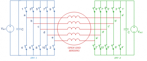
A power circuit diagram of a five-phase two-level dual VSI is shown in Figure 1 for three-level operation. Here is a positive end converter (blue inverter) referred to as INV 1 and a negative end converter (green inverter) referred to as INV 2. Five legs are composed in each inverter having two semiconductor switches in each leg i.e. IGBT, totaling ten switches. The operation of both switches on the same leg is complementary, to avoid the short-circuiting of the input DC source. The inverters' inputs are supplied with equal/unequal values from isolated dc-link sources and the outputs are connected to the open-end winding.
Figure 1. Circuit diagram of five phase two-level dual voltage source inverter
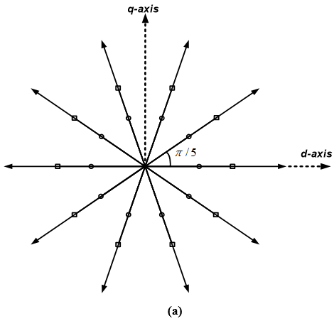
Figure 2. (a) Phase voltage space vector d-q plane; (b) Phase voltage space vectors in x-y plane
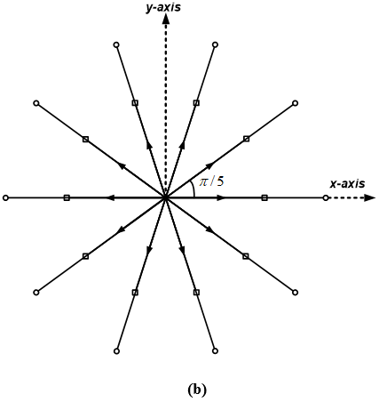
Figure 3. Voltage vector plane and voltage selection for dual inverter
Using the SVPWM scheme, each inverter in a five-phase system has thirty-two switching vectors with thirty active vectors and two zero vectors [5]. The five-phase input voltage and space vector equation are given using power invariant matrix:
$\begin{align} & {{\text{v}}_{\text{a}}}\text{=}\sqrt{\text{2}}\text{Vcos( }\!\!\omega\!\!\text{ t)} \\ & {{\text{v}}_{\text{b}}}\text{=}\sqrt{\text{2}}\text{Vcos( }\!\!\omega\!\!\text{ t-2 }\!\!\pi\!\!\text{ /5)} \\ & {{\text{v}}_{\text{c}}}\text{=}\sqrt{\text{2}}\text{Vcos( }\!\!\omega\!\!\text{ t-4 }\!\!\pi\!\!\text{ /5)} \\ & {{\text{v}}_{\text{d}}}\text{=}\sqrt{\text{2}}\text{Vcos( }\!\!\omega\!\!\text{ t+4 }\!\!\pi\!\!\text{ /5)} \\ & {{\text{v}}_{\text{e}}}\text{=}\sqrt{\text{2}}\text{Vcos( }\!\!\omega\!\!\text{ t+2 }\!\!\pi\!\!\text{ /5)} \\ \end{align}$ (1)
${{\underline{v}}_{dq}}=\frac{2}{5}({{v}_{a}}+\underline{a}{{v}_{b}}+{{\underline{a}}^{2}}{{v}_{c}}+{{\underline{a}}^{*2}}{{v}_{d}}+{{\underline{a}}^{*}}{{v}_{e}})$ (2a)
${{\underline{v}}_{xy}}=\frac{2}{5}({{v}_{a}}+{{\underline{a}}^{2}}{{v}_{b}}+{{\underline{a}}^{*}}{{v}_{c}}+{{\underline{a}}^{{}}}{{v}_{d}}+{{\underline{a}}^{*2}}{{v}_{e}})$ (2b)
where, a = exp(j2p/5), a2 = exp(j4p/5), a* = exp(-j2p/5), a*2 = exp(-j4p/5) and * stands for a complex conjugate. The phase voltage space vectors thus obtained in d-q plane using (2a) are shown in Figure 2 and since it is a five-phase system, transformation is further done to obtain space vectors in x-y plane using (2b) and the resulting space vectors are shown in Figure 3.
All the thirty active vectors have divided in three groups according to their magnitude i.e. large vectors, medium vectors and small vectors. The author has proposed two PWM schemes for the five-phase dual VSI (a) using only large vectors (b) using large and medium vectors.
The selection of switching voltage for the dual inverter having two different dc voltage sources is illustrated in Figure 3.
4.1 Using only large voltage vectors
For the generation of reference voltage vector, two neighboring large active voltage vectors, and one null voltage vector is used for every inverter [30]. The duration of time of both the active space voltage vector has presented by
${{\text{T}}_{1}}\text{=}\frac{\left| {{\underline{\text{v}}}_{\text{ref}}} \right|\text{sin}\left( \text{k }\!\!\pi\!\!\text{ /5- }\!\!\alpha\!\!\text{ } \right)}{\left| {{\underline{\text{v}}}_{\text{l}}} \right|\text{sin}\left( \text{ }\!\!\pi\!\!\text{ /5} \right)}{{\text{T}}_{\text{s}}}$ (3)
${{\text{T}}_{2}}\text{=}\frac{\left| {{\underline{\text{v}}}_{\text{ref}}} \right|\text{sin}\left( \text{ }\!\!\alpha\!\!\text{ -}\left( \text{k-1} \right)\text{ }\!\!\pi\!\!\text{ /5} \right)}{\left| {{\underline{\text{v}}}_{\text{l}}} \right|\text{sin}\left( \text{ }\!\!\pi\!\!\text{ /5} \right)}{{\text{T}}_{\text{s}}}$ (4)
${{\text{T}}_{\text{0}}}\text{=}{{\text{T}}_{\text{s}}}\text{-}{{\text{T}}_{1}}\text{-}{{\text{T}}_{2}}$ (5)
Here symbol, $\mathrm{k}=$ sector number $(\mathrm{k}=1$ to 10 for five phase $)$, $\left|\underline{v}_{l}\right|=\frac{2}{5} V_{d c} 2 \cos (\pi / 5)=$ peak of length of large voltage vector, $\underline{v}_{\mathrm{ref}}=$ reference vector, $\mathrm{l}=$ large space vectors, $\mathrm{T}_{\mathrm{s}}=$ sampling period and θ(0, π/5) = angle between Vref & V1.
Table 1. Switching sequence for the multi-level operation
|
Sector |
Switching Sequence |
||||||
|
I |
V0 |
V2 |
V1 |
V0 |
V1 |
V2 |
V0 |
|
00000 |
11000 |
11001 |
11111 |
11001 |
11000 |
00000 |
|
|
II |
V0 |
V2 |
V3 |
V0 |
V3 |
V2 |
V0 |
|
00000 |
11000 |
11100 |
11111 |
11100 |
11000 |
00000 |
|
|
III |
V0 |
V4 |
V3 |
V0 |
V3 |
V4 |
V0 |
|
00000 |
01100 |
11100 |
11111 |
11100 |
01100 |
00000 |
|
|
IV |
V0 |
V4 |
V5 |
V0 |
V5 |
V4 |
V0 |
|
00000 |
01100 |
01110 |
11111 |
01110 |
01100 |
00000 |
|
|
V |
V0 |
V6 |
V5 |
V0 |
V5 |
V6 |
V0 |
|
00000 |
00110 |
01110 |
11111 |
01110 |
10110 |
00000 |
|
|
VI |
V0 |
V6 |
V7 |
V0 |
V7 |
V6 |
V0 |
|
00000 |
00110 |
00111 |
11111 |
00111 |
10110 |
00000 |
|
|
VII |
V0 |
V8 |
V7 |
V0 |
V7 |
V8 |
V0 |
|
00000 |
00011 |
00111 |
11111 |
00111 |
00011 |
00000 |
|
|
VIII |
V0 |
V8 |
V9 |
V0 |
V9 |
V8 |
V0 |
|
00000 |
00011 |
10011 |
11111 |
10011 |
00011 |
00000 |
|
|
IX |
V0 |
V10 |
V9 |
V0 |
V9 |
V10 |
V0 |
|
00000 |
10001 |
10011 |
11111 |
10011 |
10001 |
00000 |
|
|
X |
V0 |
V10 |
V1 |
V0 |
V1 |
V10 |
V0 |
|
00000 |
10001 |
11001 |
11111 |
11001 |
10001 |
00000 |
|
During sampling time, two reference voltages generated by both the inverters are used to generate the average voltage vector. Using the proposed method, dual two-level five-phase VSI inverter performance is similar to multilevel operation as in a multi-level neutral point clamped (NPC) inverter. Another advantage of this scheme is that, along with minimizing switching losses, it minimizes the overall total harmonic distortion, the switching pattern for multilevel operations is shown in Table 1.
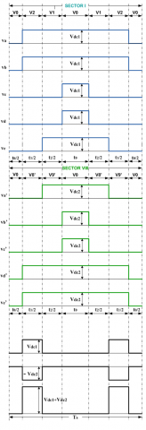
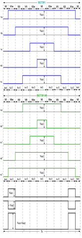
During the synthesis process both the reference voltages Vref & Vref' produced by each inverter move in all the ten sectors (I to X) in decagon vector diagram using ten active vectors for INV 1(V1 to V10) and ten active vectors for INV 2 (V1' to V10') and two null vectors (V0&V0') positioned at origin. It is a key feature to reduce the switching losses, switching, and overall THD for inverter function. The switching waveform for dual VSI for both reference voltages (Vref & Vref’) are in Figure 4(a). For greater comprehension switching pattern is presented in blue for INV 1 and green for INV 2 utilizing space vector V0, V1, V2, V0', V8', and V9' and line voltages are presented in black color during the sampling period.
4.2 Using large and medium voltage vectors
(a)
(b)
Figure 4. (a). Switching waveforms for five phase two-level dual VSI for multilevel operation using large vectors only; (b). Switching waveforms for five phase two-level dual VSI for multilevel operation using large and medium vectors
Table 2. Switching sequence for the multilevel operation using large and medium vector
|
Sector |
Switching Sequence |
||||||||||
|
I |
V0 |
V1 |
V2 |
V1 |
V2 |
V0 |
V2 |
V1 |
V2 |
V1 |
V0 |
|
00000 |
10000 |
11000 |
11001 |
11101 |
11111 |
11101 |
11001 |
11000 |
10000 |
00000 |
|
|
II |
V0 |
V3 |
V2 |
V3 |
V2 |
V0 |
V2 |
V3 |
V2 |
V3 |
V0 |
|
00000 |
01000 |
11000 |
11100 |
11101 |
11111 |
11101 |
11100 |
11000 |
01000 |
00000 |
|
|
III |
V0 |
V3 |
V4 |
V3 |
V4 |
V0 |
V4 |
V3 |
V4 |
V3 |
V0 |
|
00000 |
01000 |
01100 |
11100 |
11110 |
11111 |
11110 |
11100 |
01100 |
01000 |
00000 |
|
|
IV |
V0 |
V5 |
V4 |
V5 |
V4 |
V0 |
V4 |
V5 |
V4 |
V5 |
V0 |
|
00000 |
00100 |
01100 |
01110 |
11110 |
11111 |
11110 |
01110 |
01100 |
00100 |
00000 |
|
|
V |
V0 |
V5 |
V6 |
V5 |
V6 |
V0 |
V6 |
V5 |
V6 |
V5 |
V0 |
|
00000 |
00100 |
00110 |
01110 |
01111 |
11111 |
01111 |
01110 |
10110 |
00100 |
00000 |
|
|
VI |
V0 |
V7 |
V6 |
V7 |
V6 |
V0 |
V6 |
V7 |
V6 |
V7 |
V0 |
|
00000 |
00010 |
00110 |
00111 |
01111 |
11111 |
01111 |
00111 |
10110 |
00010 |
00000 |
|
|
VII |
V0 |
V7 |
V8 |
V7 |
V8 |
V0 |
V8 |
V7 |
V8 |
V7 |
V0 |
|
00000 |
00010 |
00011 |
00111 |
10111 |
11111 |
10111 |
00111 |
00011 |
00010 |
00000 |
|
|
VIII |
V0 |
V9 |
V8 |
V9 |
V8 |
V0 |
V8 |
V9 |
V8 |
V9 |
V0 |
|
00000 |
00001 |
00011 |
10011 |
10111 |
11111 |
10111 |
10011 |
00011 |
00001 |
00000 |
|
|
IX |
V0 |
V9 |
V10 |
V9 |
V10 |
V0 |
V10 |
V9 |
V10 |
V9 |
V0 |
|
00000 |
00001 |
10001 |
10011 |
11011 |
11111 |
11011 |
10011 |
10001 |
00001 |
00000 |
|
|
X |
V0 |
V1 |
V10 |
V1 |
V10 |
V0 |
V10 |
V1 |
V10 |
V1 |
V0 |
|
00000 |
10000 |
10001 |
11001 |
11011 |
11111 |
11011 |
11001 |
10001 |
10000 |
00000 |
|
The harmonic content is present in the output phase voltages using only large voltage vectors. This implies that, as only two active vectors are often used in each sector, we do not get satisfactory results. For a pure sinusoidal voltage waveform, the number of vectors should be one less than the number of phases [30]. This means that four active voltage vectors should be used rather than two to achieve satisfactory sinusoidal outcomes in a five-phase system. For each inverter, two neighboring large and two neighboring medium active voltage vectors are used for the generation of reference voltage vectors along with one null voltage vector. The switching waveform for dual VSI for both reference voltages (Vref & Vref’) using large and medium vectors are in Figure 4(b). The duration of time of both the active space voltage vector has presented by:
${{\text{T}}_{\text{al}}}\text{=}\frac{\left| {{\underline{\text{v}}}_{\text{l}}} \right|}{\left| {{\underline{\text{v}}}_{\text{l}}} \right|\text{+}\left| {{\underline{\text{v}}}_{\text{m}}} \right|}{{\text{T}}_{\text{a}}}$
${{\text{T}}_{\text{bl}}}\text{=}\frac{\left| {{\underline{\text{v}}}_{\text{l}}} \right|}{\left| {{\underline{\text{v}}}_{\text{l}}} \right|\text{+}\left| {{\underline{\text{v}}}_{\text{m}}} \right|}{{\text{T}}_{\text{b}}}$
${{\text{T}}_{\text{am}}}\text{=}\frac{\left| {{\underline{\text{v}}}_{\text{m}}} \right|}{\left| {{\underline{\text{v}}}_{\text{l}}} \right|\text{+}\left| {{\underline{\text{v}}}_{\text{m}}} \right|}{{\text{T}}_{\text{a}}}$
${{\text{T}}_{\text{bm}}}\text{=}\frac{\left| {{\underline{\text{v}}}_{\text{m}}} \right|}{\left| {{\underline{\text{v}}}_{\text{l}}} \right|\text{+}\left| {{\underline{\text{v}}}_{\text{m}}} \right|}{{\text{T}}_{\text{b}}}$
${{\text{T}}_{\text{0}}}\text{=}{{\text{T}}_{\text{s}}}\text{-}{{\text{T}}_{\text{al}}}\text{-}{{\text{T}}_{\text{am}}}\text{-}{{\text{T}}_{\text{bl}}}\text{-}{{\text{T}}_{\text{bm}}}$
All the symbols have its usual meaning. Switching pattern for multilevel operation using large and medium vector is displays in Table 2.
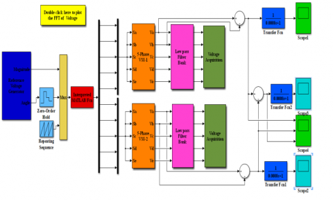
Figure 5 shows the Matlab/Simulink model for the dual five-phase voltage source inverter for multilevel output in which the first block shows the generation of reference voltage. Magnitude and angle are the output of this block. This provides the switching signal for different semiconductors of voltage source inverter block devices with the help of Matlab code, repeating sequence signal, and zero-order hold circuit. The output of this block is stored in five-phase voltages in the voltage acquisition block workspace after passing through the low-pass filter block.
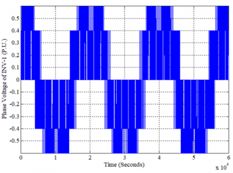
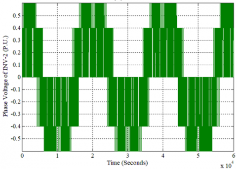
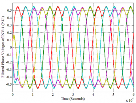
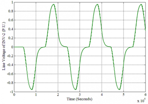
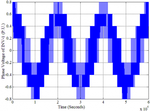
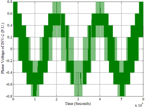
Figures 6(a) and 6(b) are showing the output phase voltages for INV 1 and INV 2 using only large vectors. Figure 7 displays filtered phase voltages of INV-1. The output voltages possess sufficient amount of third order harmonic along with small amount of 7th order harmonic. These harmonics are generated due to x-y components of space voltage vectors and will present in output whatever the reference voltage value may be when only large vectors are utilized to control the output of inverter. Figure 8 shows the filtered line voltages for INV 2.
Phase-to-Neutral value of Voltage Space Vectors for large vector and for medium vector is given by Eq. (6) and (7) respectively.
$\begin{align} & \left| {{\underline{\text{v}}}_{1}} \right|\text{=}2/5{{V}_{DC}}2\cos (\pi /5)\exp (jk\pi /5)\text{ } \\ & \text{for }k=0,1,\cdots 9 \\ \end{align}$ (6)
$\begin{align} & \left| {{\underline{\text{v}}}_{\text{m}}} \right|=2/5{{V}_{DC}}\exp (jk\pi /5)\text{ } \\ & \text{for }k=0,1,2\cdots 9 \\\end{align}$ (7)
Adjacent Line-to-Line value of Voltage Space Vectors for large vector and for medium vector is given by Eq. (8) and (9) respectively.
$\begin{align} & \left| {{{\underset{\scriptscriptstyle-}{V}}}_{1}} \right|=\sqrt{1.382}* \\ & 2/5{{V}_{DC}}2\cos (\pi /5)\exp (j(2k+1)\pi /10) \\ & \text{for }k=1,2\cdots 9 \\ \end{align}$ (8)
$\begin{align} & \left| {{{\underset{\scriptscriptstyle-}{V}}}_{m}} \right|=\sqrt{0.528}* \\ & 2/5{{V}_{DC}}2\cos (\pi /5)\exp (j(2k+1)\pi /10) \\ & \text{for }k=1,2\cdots 9 \\ \end{align}$ (9)
Figure 5. Matlab/Simulink Model of dual five-phase VSI
(a)
(b)
Figure 6 (a). Phase voltage of INV-1; (b). Phase voltage of INV-2
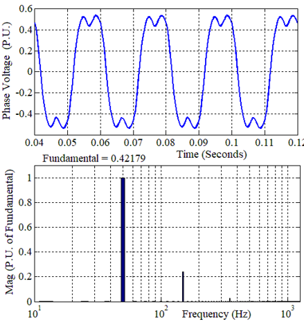
The dc-link voltage parameter is kept unity whereas switching frequency and fundamental frequency are 2 kHz and 50 Hz for simulation. Figure 9 shows the harmonic output spectrum for the voltage 'a' phase. It only has a fundamental voltage with a magnitude of 0.4218 p.u. r.m.s at a frequency of 50 Hz. The total harmonic distortion (THD) in the output is 23.97% and weighted total harmonic distortion (WTHD) is 12.46% of the fundamental, which shows that the results near the sinusoidal.
Simulation results for three-level operation using large and medium voltage vectors are in Figure 10 to Figure 12. Figures 10(a) and 10(b) display the phase voltages for INV-1 and INV-2 and Figure 11 show the filtered phase voltages for INV1. While Figure 12 shows the filtered line voltage for INV 2. All the parameters for simulation are kept the same.
Figure 7. Filtered phase voltage of INV-1
Figure 8. Filtered line voltage of INV-2
Figure 9. Harmonic spectrum of inverter output phase voltage
(a)
(b)
Figure 10. (a). Phase voltage of INV-1; (b). Phase voltage of INV-2
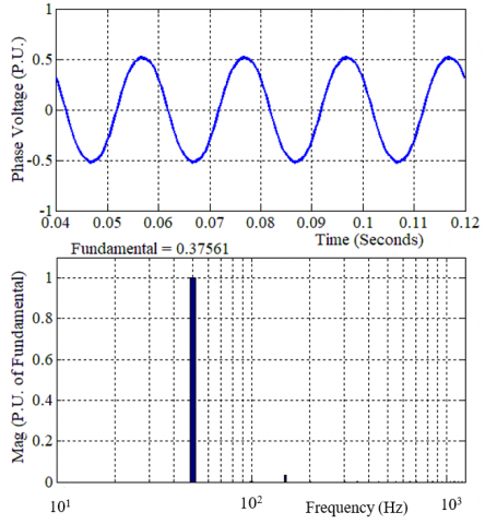
Figure 13 exhibits the harmonic spectrum of output for phase ‘a’ voltage. It contains only fundamental voltage having magnitude of 0.3756 p.u. r.m.s at a frequency of 50 Hz. The total harmonic distortion (THD) in the output is 3.30% and weighted total harmonic distortion (WTHD) is 1.81% of the fundamental, which is very less as compared to the previous scheme.
Figure 11. Filtered phase voltage of INV-1
Figure 12. Filtered line voltage of INV-2
Figure 13. Harmonic spectrum of inverter output phase voltage
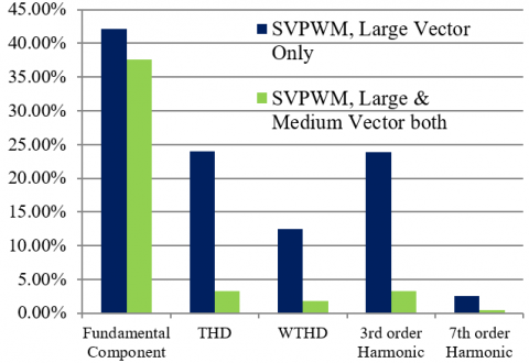
In accordance with the fundamental Component, THD, and WTHD, the contribution of both the presented SVPWM scheme has been examined and a comparative analysis has been concluded. The comparison of both SVPWM schemes is shown in Table 3 and Figure 14 is showing the bar chart for quick comprehension. It is clear here that, compared to the first SVPWM scheme, the scheme using large and medium voltage vectors has very low order harmonic content.
The time of application of large and medium vectors is proportionally divided according to their length. The first system offers sinusoidal efficiency, but only up to 85.41% of the total achievable basic output is operational. The second scheme makes it possible to fully utilise the available DC bus voltage. It is known that the highest reference value to be reached is between 85.41% and 100%. The inverter's reference voltage exceeds the maximum output circle because of this. The application time of different voltage vectors is dependent on the voltage and variable amplitude of the reference voltage.
The study shows that using only large vectors to validate the concept, the output contains 23.97% THD and 12.46% WTHD, which indicates that the losses are substantial. It is because the output contains a sufficient amount of 3rd order harmonics i.e. 23.8349% and a small amount of 7th order harmonics i.e. 2.504650%.
When the author uses the large and medium vectors together, the results are much better compared to the previous scheme to reduce THD. The output includes 3.30% THD and 1.81% WTHD only using large and medium vectors. 3rd order harmonics decrease from 23.834% to 3.2474% and 7th order harmonic has reduced to 2.50% to 0.436947%
Table 3. Comparison of both the SVPWM Schemes
|
Description |
using large vector only |
using large & medium vectors |
|
Fundamental Component |
42.18% |
37.56% |
|
Total Harmonic Distortion |
23.97% |
3.30% |
|
Weighted Total Harmonic Distortion |
12.46% |
1.81% |
|
3rd order Harmonic |
23.834900% |
3.247490% |
|
7th order Harmonic |
2.504650% |
0.436947% |
Figure 14. Bar chart of both SVPWM scheme
In this paper, two SVPWM schemes for a two-level five-phase dual voltage source inverter are presented to achieve multilevel performance. The first scheme is by using large vectors only, which generates the non-sinusoidal output results due to significant low-order harmonics presence. Another approach utilizes both large and medium voltage vectors to obtain sinusoidal output results, which shows that as compared to the first scheme, the second technique has low values of low-order harmonics. These SVPWM techniques are easy and effective to implement. The presented schemes may apply easily in high power medium voltage applications. A similar concept may be extended to a higher phase number inverter system in the future along with a practical realization.
|
SVPWM |
Space Vector pulse width modulation |
|
VSI |
Voltage source inverter |
|
THD |
Total harmonic distortion |
|
WTHD |
Weighted total harmonic distortion |
|
NPC |
Neutral point clamped |
[1] Singh, G.K. (2002). Multi-phase induction machine drive research—a survey. Electric Power Systems Research, 61(2): 139-147. https://doi.org/10.1016/S0378-7796(02)00007-X
[2] Jones, M. (2002). A literature survey of state-of-the-art in multiphase ac drives. In Conf. Rec. Universities Power Engineering Conf. UPEC, 2002.
[3] Ward, E.E., Härer, H. (1969). Preliminary investigation of an invertor-fed 5-phase induction motor. In Proceedings of the Institution of Electrical Engineers 116(6): 980-984. https://doi.org/10.1049/piee.1969.0182
[4] Holmes, D.G., Lipo, T.A. (2003). Pulse Width Modulation for Power Converters: Principles and Practice. 18: John Wiley & Sons.
[5] Iqbal, A., Levi, E. (2005). Space vector modulation schemes for a five-phase voltage source inverter. In 2005 European Conference on Power Electronics and Applications, 12. https://doi.org/10.1109/EPE.2005.219194
[6] Iqbal, A., Levi, E. (2006). Space vector PWM techniques for sinusoidal output voltage generation with a five-phase voltage source inverter. Electric Power Components and Systems, 34(2): 119-140. https://doi.org/10.1080/15325000500244427
[7] Zhao, Y., Lipo, T.A. (1995). Space vector PWM control of dual three-phase induction machine using vector space decomposition. IEEE Transactions on Industry Applications, 31(5): 1100-1109. https://doi.org/10. 1109/28.464525
[8] Chai, M., Xiao, D., Dutta, R., Fletcher, J.E. (2015). Space vector PWM techniques for three-to-five-phase indirect matrix converter in the overmodulation region. IEEE Transactions on Industrial Electronics, 63(1): 550-561. https://doi.org/10.1109/ TIE. 2015.2475416
[9] Elgenedy, M.A., Elserougi, A.A., Abdel-Khalik, A.S., Massoud, A.M., Ahmed, S. (2015). A space vector PWM scheme for five-phase current-source converters. IEEE Transactions on Industrial Electronics, 63(1): 562-573. https://doi.org/10.1109/TIE.2015.2493514
[10] Rodríguez, J., Bernet, S., Wu, B., Pontt, J.O., Kouro, S. (2007). Multilevel voltage-source-converter topologies for industrial medium-voltage drives. IEEE Transactions on Industrial Electronics, 54(6): 2930-2945. https://doi.org/10.1109/TIE.2007.907044
[11] Rodriguez, J., Lai, J.S., Peng, F.Z. (2002). Multilevel inverters: A survey of topologies, controls, and applications. IEEE Transactions on Industrial Electronics, 49(4): 724-738. https://doi.org/10.1109/TIE.2002.801052
[12] El-Saady, G., Ibrahim, E.N.A., Elbesealy, M. (2013). V/f control of three phase induction motor drive with different PWM techniques. Innovative Systems Design and Engineering, 4(14): 131-144.
[13] Gopakumar, K., Ranganathan, V.T., Bhat, S.R. (1993). An efficient PWM technique for split phase induction motor operation using dual voltage source inverters. In Conference Record of the 1993 IEEE Industry Applications Conference Twenty-Eighth IAS Annual Meeting, pp. 582-587. https://doi.org/10.1109/IAS.1993.298982
[14] Somasekhar, V.T., Gopakumar, K., Pittet, A., Ranganathan, V.T. (2001). A novel PWM inverter switching strategy for a dual two-level inverter fed open-end winding induction motor drive. In 4th IEEE International Conference on Power Electronics and Drive Systems. IEEE PEDS 2001-Indonesia. Proceedings (Cat. No. 01TH8594), 1: 196-202. https://doi.org/10.1109/PEDS.2001.975310
[15] Shivakumar, E.G., Gopakumar, K., Sinha, S.K., Pittet, A., Ranganathan, V.T. (2001). Space vector PWM control of dual inverter fed open-end winding induction motor drive. In APEC 2001. Sixteenth Annual IEEE Applied Power Electronics Conference and Exposition (Cat. No. 01CH37181), 1: 399-405. https://doi.org/10.1109/APEC.2001.911678
[16] Ramachandrasekhar, K., Mohan, S., Srinivas, S. (2010, September). An improved PWM for a dual two-level inverter fed open-end winding induction motor drive. In the XIX International Conference on Electrical Machines-ICEM, pp. 1-6. https://doi.org/10.1109/ICELMACH.2010.5607866
[17] Somasekhar, V.T., Gopakumar, K., Shivakumar, E.G. (2002). A space-vector modulation scheme for a dual two-level inverter fed open-end winding induction motor drive for the elimination of zero-sequence currents. Epe Journal, 12(2): 1-19. https://doi.org/10.1080/ 09398368. 2002.11463502
[18] Somasekhar, V.T., Srinivas, S., Gopakkumar, K. (2005). A space vector based PWM switching scheme for the reduction of common-mode voltages for a dual inverter fed open-end winding induction motor drive. In 2005 IEEE 36th Power Electronics Specialists Conference, pp. 816-821. https://doi.org/10.1109/ PESC. 2005.1581721
[19] Kalaiselvi, J., Sekhar, K.R.C., Srinivas, S. (2012). Common mode voltage elimination PWMs for a dual two-level VSI with single inverter switching. In 2012 IEEE International Symposium on Industrial Electronics, pp. 234-239. https://doi.org/10.1109/ISIE.2012.6237090
[20] Sekhar, K.R., Srinivas, S. (2012). Discontinuous decoupled PWMs for reduced current ripple in a dual two-level inverter fed open-end winding induction motor drive. IEEE Transactions on Power Electronics, 28(5): 2493-2502. https://doi.org/10.1109/TPEL.2012.2215344
[21] Chen, M., Sun, D. (2016). A unified space vector pulse width modulation for dual two-level inverter system. IEEE Transactions on Power Electronics, 32(2): 889-893. https://doi.org/10.1109/TPEL.2016.2585223
[22] Lavanya, M., Jyothi, B. 2(016). Performance analysis of 5-phase multi-level inverter using carrier based PWM technique. International Journal of Applied Power Engineering (IJAPE), 5(3): 151-158. https://doi.org/10.11591/ijape.v5.i3.pp151-158
[23] Jyothi, B., Rao, M.V.G. (2017). Performance Analysis of 3-Level 5-Phase Multilevel Inverter Topologies. International Journal of Electrical and Computer Engineering, 7(4): 1696. https://doi.org/10.11591/ijece.v7i4
[24] Lihitkar, S., Rangari, S. (2018, June). Comparative study of IPD and POD for three level five phase inverter. In 2018 International Conference on Smart Electric Drives and Power System (ICSEDPS), pp. 313-316. https://doi.org/10.1109/ ICSEDPS.2018.8536047
[25] Raja, D., Ravi, G. (2018). Comparative analysis of five phase multilevel inverter topologies for five phase induction motor drive. Journal of Advanced Research in Dynamical and Control Systems, 09-Special Issue: 1961-1968.
[26] Raja, D., Ravi, G. (2018). New switch ladder topology for five phase multilevel inverter fed five phase induction motor. In 2018 International Conference on Recent Innovations in Electrical, Electronics & Communication Engineering (ICRIEECE), pp. 1358-1362. https://doi.org/10.1109/ICRIEECE44171.2018.9008869
[27] Sajitha, M., Ramchand, R. (2019). Space vector PWM scheme for three phase three level t-type NPC inverter. In 2019 2nd International Conference on Intelligent Computing, Instrumentation and Control Technologies (ICICICT), 1: 523-528. https://doi.org/10.1109/ICICICT46008. 2019. 8993215
[28] Ramasamy, P., Krishnasamy, V. (2020). Minimization of Common-Mode Voltage for Five-Phase Three-Level NPC Inverter Using SVPWM Strategy. Iranian Journal of Science and Technology, Transactions of Electrical Engineering, 44(3): 1221-1232. https://doi.org/10.1007/s40998-019-00304-5
[29] Usha, S., Geetha, A., Thentral, T.T., Subramani, C., Venkatesan, M. (2020). Mitigation of common mode voltage in five phase multilevel inverter. Materials Today: Proceedings. https://doi.org/10.1016/j.matpr.2020.08.625
[30] Kelly, J.W., Strangas, E.G., Miller, J.M. (2003). Multiphase space vector pulse width modulation. IEEE Transactions on Energy Conversion, 18(2): 259-264. https://doi.org/10.1109/TEC.2003.811725