Neerja Singh | Gaurav Verma* | Vijay Khare
© 2022 IIETA. This article is published by IIETA and is licensed under the CC BY 4.0 license (http://creativecommons.org/licenses/by/4.0/).
OPEN ACCESS
Nowadays, the main challenge in front of system designers is to design power-efficient systems with reduced design turnaround time. It can be achieved in two ways, firstly, utilize off-shelf components (Intellectual Property cores) along with user-defined IPs. Secondly, estimate the power at an early stage of the design cycle. Therefore, this paper represents the power estimation of Cascaded and Non-Cascaded DSP blocks based on IP modeling. The DSP blocks are designed using a blend of embedded and user-defined IP cores. Curve-fitting and regression-based models for power evaluation have been created for each IP core. The power of the complete DSP block is estimated using identity projected by Elleouet et al. by incorporating the power values of each IP core obtained from the regression-based models. The models have been validated for accuracy using the power values gained from the commercial tool (Vivado design suite (2014.2)). From the analysis, it has been found that the identity is providing inaccurate results for cascaded DSP blocks. Therefore, in this work, a new identity has been proposed that has been estimating the power of the cascaded systems accurately and also in alignment with the results of a commercial tool.
FIR, IP, DSP, power, FPGA, RTL
The foremost consequence of transistor miniaturization is high power consumption. This has led to the additional requirement of cooling devices and has also reduced battery life. Currently, power is the critical constraint for electronic design engineers with compressed design schedules. Nowadays, reconfigurable circuits such as FPGAs have preferred technology as they can achieve high performance with low cost and lesser time consumption [1]. These devices can implement complex circuits such as DSP blocks and embedded memories [2]. Today, these devices are attractive alternatives to their Application-Specific Integrated Circuits (ASICs) counterparts. But, due to their increased complexity, power consumption has aroused as the constraining factor that has bounded FPGA designs to cross the threshold of low power applications.
Several power estimation techniques already exist in the literature, but, accurate power estimation is possible only with the knowledge of capacitances. The available commercial tool measures the power accurately, but, with a longer time penalty. Power assessment at a higher abstraction level is not much accurate because of the absence of low-level statistics. So, to overcome the above-mentioned problem, system designing at Register Transfer Level (RTL) can be an attractive choice because of less simulation run time and technology independency. Though, numerous models are present in the literature that could determine the power of an individual block at the RTL level but the research on methodologies that could approximate the power of a complete system accurately using IP modeling approach, needs exploration.
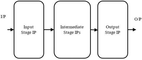
Therefore, in this paper, DSP blocks have been designed and analyzed for power using IP cores. DSP blocks have been categorized as cascaded blocks and non- cascaded blocks. In cascaded blocks, input is applied at one IP core whose output acts as the input to the intermediate IP cores, and the final output is taken at another end. In non-cascaded blocks, external input may be applied to the intermediate blocks, and output is taken at each stage. The most important advantage of system designing using different IP cores is that dedicated IP cores can be used to design many systems. This approach will undoubtedly increase the design efficiency [3]. Also, power assessment at the primary design phase will help designers to design power-efficient systems with a lesser design calendar.
The paper has been ordered in the following sequence: a review on power modeling and estimation techniques for FPGAs is deliberated in part 2, and then the flow of the proposed power estimation method is conferred in part 3. Power in FPGAs is particularized in part 4. Characterization of DSP blocks is discussed in part 5. The regression model of sub-modules used in designing each DSP block is elaborated in part 6. Power modeling of the complete system is explained in part 7. Finally, result analysis, execution time comparison, model compatibility at different frequencies and conclusion are presented in part 8, 9,10 and 11 respectively.
Elleouet et al. [3] have anticipated an identity that could estimate the power of a system designed using N IP cores. Architectural and algorithmic parameters have been used for projecting the model. The analysis is based at the system level. Jevtic et al. [4] have proposed a model that could estimate the power of multiplier blocks in FPGAs. They discovered a void in David Elleouet and Nathalie Choy’s work. According to their detections, interconnect and component powers have not been divided separately which may cause accuracy issues for complex designs. Lorandel et al. [5] have presented a method that could evaluate the power of wireless communication systems at a higher abstraction level. The proposed methodology is specific to a wireless communication system. Also, in their work emphasis has not been put on how the power is influenced after interconnecting various IP blocks. Deng et al. [6] have presented curve-fitting and regression-based models that could accurately estimate the area, time and power. Their work is on IP cores-based implementations for FPGAs. This designing approach will greatly enhance the hardware development efficiency. Gebotys et al. [7] have presented a linear regression-based model that could predict the power. They derived variables from the DSP code for formulating the models and achieved an error of less than 4%. Verma et al. [8] have applied the statistical power estimation technique for estimating the power of embedded systems. The analysis has been carried out for almost 30 circuits and power has been estimated using Xpower Analyzer. They found that the statistical-based power estimation technique provides good accuracy with a faster estimation speed. Nasser et al. [9] in their paper have presented an overview of power modeling and estimation techniques at different abstraction levels (from RTL to the transistor). They found that the simulation-based estimation technique is generic and estimates power accurately with a longer estimation time. However, the probabilistic-based approach provides low accuracy, but higher estimation speed. Referring to various works, they also agreed to the fact that the statistical-based estimation technique provides moderate accuracy with moderate estimation speed. Raghunathan et al. [10] have proposed a statistical modeling technique at the RTL level that could estimate switching activity and power consumption. In their work, they have considered glitches to achieve better accuracy. An error of about 7% has been achieved. Makani et al. [11] worked on resource utilization report from hardware. They carry out analysis for estimating the area and power without RTL implementation. Durrani and Riesgo [12] have proposed a modeling technique at the architectural level that could estimate the power based on the knowledge of input/output. Similar to Elleouet et al. [3] they have also claimed that the fast power estimation of IP-based designs can be achieved by simply adding the power consumed by the individual IP cores. They have achieved the error of 1-2% for individual macro-blocks and 9-15% for the complete system. They have also not focused on how the power would get influenced once the various IP blocks are interconnected to form a complete system. Singh et al. [13] have proposed Artificial Neural Network (ANN) and regression-based model for an embedded multiplier. As per their finding the proposed models are generic for all 7-series FPGAs devices. Therefore, in this work, while designing a complete system using different IP cores, the focus has been laid on interconnection power.
From the literature survey, it has been analyzed that various power modeling and estimation techniques have been established in literature at a different abstraction level. It has been seen that the statistical based modeling technique is providing better accuracy and estimation speed. Various works have been reported in the literature for power estimation at RTL level, but it is limited to individual blocks only. Very few works have been reported related to IP modelling approach for complete system. Therefore, power estimation of systems designed using IP cores is still in the primary phase. Thus, power estimation at RTL level based on IP modeling can prove to be an exceptional profusion due to technology independence and lesser simulation run-time.
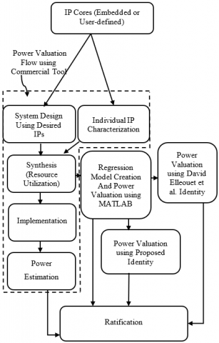
The proposed power estimation flow is shown in Figure 1. In this work, DSP blocks are designed by interconnecting diverse IP cores. DSP blocks are intended to use desired embedded as well as user-defined IP cores. User-defined IP cores are incorporated into the library using Verilog Hardware Descriptive Language (HDL). After design implementation, the value of total power is generated. Individual IP cores are modified and synthesized for various Input/Output (I/O) configurations. Data obtained after post synthesis has been used for creating regression-based model for individual IP cores.
Figure 1. Power estimation process
System power is estimated through identity proposed by David et al. and proposed identity in this work using power values obtained from the regression model. The assessed power values from the commercial tool have been referred for authenticating the power values gained from identity proposed by Elleouet et al. [3] and the proposed identity in this work.
In FPGAs, the power consumption has increased due to the large count of programmable switches and interconnects. The total power, Power(T) in FPGA is sum of static power, Power(S) and dynamic power, Power(D) as given by Eq. (1).
${Power}_{(T)}={Power}_{(D)}+{Power}_{(S)}$ (1)
Static power is not instantaneous for a particular FPGA device and it occurs due to leakage mechanism in MOS transistors, and leakage mechanism itself is a function of the temperature. In this work, no significant rise is observed in temperature while analysis, hence the static power is assumed to be constant i.e., 120mW. However, dynamic power change instantly and is given by Eq. (2).
$\operatorname{Power}_{(D)}=\alpha \times f_{c l k} \times C_L \times V_{D D}{ }^2$ (2)
where, CL is the total capacitance, VDD is the supply voltage, α is the switching activity and fclk is the clock frequency as per the design requirement [14-18]. Vivado tool estimate the value of α at various nodes of circuit under consideration using a vector-less algorithm. So, control over α is not possible when circuits are designed by interconnecting various IP blocks. Hence, in FPGAs, dynamic power can be given by Eq. (3).
$Power_D=( Signal + Logic +I / O+ Clock+ Memory +D S P) Power$ (3)
where, I/O power depends on the total number of input/output pins. The average power disbursed by the clock web is the clock power. This also includes power spent by buffer and routing resources. Average power spent by interconnects is termed as the signal power. Logic power is a function of Configurable Logic Blocks (CLBs). This includes power spent by Look-up- Tables (LUTs) and Flip-Flop (FF). Memory power depends upon memory elements. DSP power is a function of number of DSP blocks used in the particular design [5].
In this work, various DSP blocks have been used for analyzing the feasibility of the proposed identity. DSP blocks are categorized into cascaded and non- cascaded blocks as shown in Table 1. In cascaded blocks, input is applied at one IP core whose output acts as the input to the intermediate IP cores and final output is taken at another end. In non-cascaded blocks, external input may be applied to the intermediate blocks and output is taken at each stage [19].
Table 1. Categorization of DSP blocks
|
S. No. |
Cascaded Blocks |
Non-cascaded Blocks |
|
1 |
FIR Filter |
Carry Ripple Adder |
|
2 |
MAC Unit |
Carry Skip Adder |
|
3 |
ALU |
SIPO |
|
4 |
Barrel Shifter |
PIPO |
|
5 |
Carry Save Adder |
PISO |
|
6 |
SISO |
---- |
The DSP blocks are designed by connecting embedded IPs and user-defined IPs. The architectural details of the various DSP block designed in this work is depicted in Table 2.
Table 2. Architectural details of DSP blocks
|
S. No. |
Cascaded Blocks |
Embedded IP used |
User-defined IP |
|
1 |
FIR Filter |
Four Multiplier, Three Adder |
Three Delay Element |
|
2 |
MAC Unit |
8- bit Multiplier, 16- bit Accumulator and 16- bit Adder |
None |
|
3 |
ALU |
8- bit divider, 8- bit adder/subtracter, 8 -bit multiplier |
8 -bit AND, OR, XOR, NOT gates and 16- bit MUX |
|
4 |
Barrel Shifter |
None |
Twenty-four 2:1 MUX |
|
5 |
Carry Save Adder |
None |
Eight full adder IP |
|
6 |
SISO |
None |
Four D flip-flop IP |
|
|
|||
|
S. No. |
Non-cascaded Blocks |
Embedded IP used |
User-defined IP |
|
1 |
Carry Ripple Adder |
None |
Four full adder IP |
|
2 |
Carry Skip Adder |
None |
Four full adder IP and a 2:1 MUX IP |
|
3 |
SIPO |
None |
Four D flip-flop IP |
|
4 |
PIPO |
None |
Four D flip-flop IP and four 2:1 MUX IP |
|
5 |
PISO |
None |
Four D flip-flop IP |
Curve-fitting and regression-based model for individual IP cores have been created based on the resource utilization data obtained after synthesis [20-22]. In this work, curve fitting and regression techniques is used to predict the relationship between the dependent and independent variables. Each model has been tested for accuracy against commercial tool. Parameters used and their connotation is explained in Table 3.
Table 3. Parameters used and their connotation
|
Used parameters |
Connotation |
|
out_pin |
Total output pins |
|
lut |
Total LUT (logic slice) |
|
ff |
Total Flip-Flops |
|
DSP48 |
Total DSP blocks |
6.1 Regression model for divider
Divider IP is instantiated using different configuration. The dynamic power equations obtained using curve-fitting and regression technique are given by Eq. (4) to Eq. (7). Power obtained for different divider configuration is given in Table 4.
$Outputpower =1.185 \times out\_pin -1.308$ (4)
$Clockpower =-2.437+0.1583 \times lut -0.0548 \times f f$ (5)
$Logicpower =1.475-0.0428 \times l u t+0.0232 \times {ff}$ (6)
$Signalpower =0.2327+0.003029 \times lut +0.008581 \times f f$ (7)
Table 4. Comparative analysis of embedded divider block
|
Divider configurations |
Estimated power values from commercial tool (mW) |
Estimated power values from regression-based model (mW) |
% Error |
|
8 |
145 |
145.5 |
0.36 |
|
10 |
165 |
168.25 |
1.97 |
|
12 |
168 |
171.85 |
2.28 |
|
14 |
173 |
175.94 |
1.70 |
|
16 |
180 |
180.44 |
0.25 |
|
20 |
206 |
209.58 |
1.74 |
|
24 |
215 |
221.18 |
2.87 |
|
32 |
265 |
269.13 |
1.56 |
The power values gained from regression model has been tested for accuracy with reference to the commercial tool using Eq. (8).
${Error}(\%)=\left|\left(\frac{e_i-r_i}{r_i}\right)\right| \times 100$ (8)
where, ei is the measured power from regression-based model [14]. ri is the power value gained from the Vivado tool. Other IP cores have also been validated using same method. From the analysis it has also been seen that the contribution of input power that depends on the number of input pins in the design is less than 1% to the total power. Thus, while modeling it has been assumed to be zero.
6.2 Regression model for 8:1 MUX
Mux IP is instantiated using different configuration. The dynamic power equation obtained using curve-fitting and regression technique are given by Eq. (9) to Eq. (12). The comparative analysis of 8:1 MUX IP for different configuration is given in Table 5.
Table 5. Comparative analysis of MUX block
|
8:1 MUX configurations |
Estimated power values from commercial tool (mW) |
Estimated power values from regression-based model (mW) |
% Error |
|
1 |
125 |
130.73 |
4.58 |
|
2 |
130 |
133.33 |
2.56 |
|
4 |
140 |
139.96 |
0.02 |
|
8 |
161 |
160.99 |
0.006 |
|
16 |
202 |
200.99 |
0.50 |
$Outputpower \left.=79.76 \times \exp ^{\left(-\frac{ { out\_pin }{-}18.23}{11.88} \quad \right)}\right.^2$ (9)
$Clockpower =1.42 e^{-15} \times( { lut })^{8.831}+0.9989$ (10)
$Signalpower=20.41 \times \exp ^{\left(-\frac{ { lut-36 }}{6.91} \quad \right)^2}$ (11)
$Logicpower =20.41 \times \exp \left(-\frac{l u t-36}{6.91}\right)^2$ (12)
6.3 Regression model for full adder
Full adder IP has been used in many designs. The IP is instantiated using different configuration. The dynamic power equation obtained using curve-fitting and regression technique are given by Eq. (13) to Eq. (16). The comparative analysis for different configuration is given in Table 6.
Table 6. Comparative analysis of full adder block
|
Full adder configurations |
Estimated power values from commercial tool (mW) |
Estimated power values from regression-based model (mW) |
% Error |
|
1 |
122 |
122.23 |
0.19 |
|
2 |
123 |
122.75 |
0.20 |
|
4 |
124 |
123.82 |
0.15 |
|
8 |
126 |
125.93 |
0.05 |
|
12 |
128 |
128.05 |
0.04 |
|
16 |
130 |
130.16 |
0.13 |
|
24 |
135 |
134.40 |
0.44 |
|
32 |
140 |
138.64 |
0.97 |
$Outputpower =0.5294 \times out\_pin +0.1688$ (13)
$Logicpower =0.0001$ (14)
$Signalpower =0.0001$ (15)
$Clockpower =1$ (16)
6.4 Regression model for multiplier
Multiplier IP is instantiated using different configuration. The dynamic power equation obtained using curve-fitting and regression technique are given by Eq. (17) to Eq. (20). The comparative analysis report for multiplier IP can be referred from [14].
$Outputpower =1.171 \times out\_pin -2.18$ (17)
$\begin{aligned} { DSPpower }&=3.372-5.57 \times \cos (D S P 48 \times 0.3927) \\ &+2.671 \times \sin (D S P 48 \times 0.3927) \\ &+2.04 \times \cos (2 \times D S P 48 \times 0.3927) \\ &+0.965 \times \sin (2 \times D S P 48 \times 0.3927) \end{aligned}$ (18)
$\begin{aligned} { Clockpower }=& 0.6464-0.5 \times \cos (f f \times 0.0462) \\ &+1.207 \times \sin (f f \times 0.0462) \\ &+0.85 \times \cos (2 \times f f \times 0.0462) \\ &-0.146 \times \sin ((2 \times f f \times 0.0462)\end{aligned}$ (19)
$Signalpower =2.446 \times e^{(0.0103 \times f f)}-1.646 \times e^{(-1.191 \times f f)}$ (20)
6.5 Regression model for 2:1 MUX
This IP has been customized for different input configuration. Curve-fitting and regression techniques have been applied for creating model based on synthesis report. Dynamic power equations are given by Eq. (21) to Eq. (24). The comparative analysis for different configurations is given in Table 7.
$Outputpower =0.3069 \times out\_pin +0.2721$ (21)
$Clockpower =8.375 e 14+0.03299 \times f f-8.375 e 14 \times l u t$ (22)
$Logicpower =0.0001$ (23)
$Signalpower =1$ (24)
Table 7. Comparative analysis of 2:1 MUX block
|
MUX configurations |
Estimated power values from commercial tool (mW) |
Estimated power values from regression-based model (mW) |
% Error |
|
1 |
121 |
121.95 |
0.78 |
|
4 |
122 |
122.62 |
0.51 |
|
8 |
123 |
123.97 |
0.79 |
|
16 |
126 |
126.68 |
0.54 |
|
32 |
132 |
132.09 |
0.07 |
|
48 |
137 |
137.63 |
0.46 |
|
64 |
144 |
143.04 |
0.67 |
6.6 Regression model for adder/subtractor
Adder/subtractor IP is instantiated using different configurations. The dynamic power equation obtained using curve-fitting and regression technique are given by Eq. (25) to Eq. (28). The comparative analysis result of delay IP for different configuration can be referred from [14].
$Outputpower =0.8744 \times (out\_pin )-0.2083$ (25)
$Clockpower =1-0.0147 \times lut +0.0147 \times f f$ (26)
$Signalpower =1.167+2.039 \mathrm{e} 14 \times {ff}-2.039 \mathrm{e} 14 \times lut$ (27)
$Logicpower =0.0001$ (28)
6.7 Regression model for AND gate
IP is instantiated using different configuration. Model has been created based on synthesis report. The dynamic power equation obtained using curve-fitting and regression technique are given by Eq. (29) to Eq. (32). This model is also applicable for OR gate, XOR gate and NOT gate used in the ALU design. Comparative analysis for different configuration is given in Table 8.
$Outputpower =4.769 \times out\_pin -0.2205$ (29)
$Logicpower =-213.9 \times \exp^{(-2.683 \times lut )}+1.001$ (30)
$Clockpower =8.007-5.005 \times \cos ( lut \times 0.0938)$$-3.231 \times \sin ($ lut $\times 0.0938)$
$-1.582 \times \cos (2 \times lut \times 0.0938)-0.02673 \times {Sin}(2 \times lut \times 0.0938)$ (31)
$\begin{aligned} { Signalpower }=& 0.9166-0.177 \times \cos ( { lut } \times 0.1848) \\ &-0.1096 \times \sin ( { lut } \times 0.1848) \\ &-0.3403 \times \cos (2 \times \ { lut } \times 0.1848) \\ &-0.6834 \times \sin (2 \times { lut } \times 0.1848) \end{aligned}$ (32)
Table 8. Comparative analysis of AND gate block
|
AND gate configurations |
Estimated power values from commercial tool (mW) |
Estimated power values from regression-based model (mW) |
% Error |
|
4 |
140 |
139.86 |
0.09 |
|
8 |
160 |
159.91 |
0.05 |
|
16 |
199 |
200.09 |
0.55 |
|
32 |
282 |
280.38 |
0.57 |
|
48 |
362 |
359.69 |
0.63 |
|
64 |
442 |
437.99 |
0.91 |
6.8 Regression model for delay
Delay element is created using D FF. The delay IP has been modified for different input vector length. The dynamic power equation obtained are given by Eq. (33) to Eq. (36). The comparative analysis result of delay IP for different configuration can be referred from [14].
$\begin{aligned} { Outputpower }=&-4.732 e-6 \times( { out\_pin })^4 \\ &+0.0006839 \times( { out\_pin })^3 \\ &-0.03175 \times( { out\_pin })^2 \\ &+0.5956 \times( { out\_pin })-1.965 \end{aligned}$ (33)
$Clockpower=-1.517-0.2191 \times lut +0.388 \times {ff}$ (34)
$Logicpower =0.0001$ (35)
$Signalpower =0.2241-0.1043 \times f f+0.07425 \times lut$ (36)
6.9 Regression model for accumulator
Table 9. Comparative analysis of embedded accumulator block
|
Accumulator configurations |
Estimated power values from commercial tool (mW) |
Estimated power values from regression-based model (mW) |
% Error |
|
8 |
130 |
131.1582 |
0.89 |
|
16 |
140 |
140.7182 |
0.51 |
|
24 |
150 |
150.2782 |
0.18 |
|
32 |
161 |
159.8382 |
0.72 |
|
48 |
181 |
178.9582 |
1.12 |
|
64 |
202 |
198.0782 |
1.9 |
The accumulator is customized for different output width. Analytical model has been created using post synthesis report. Equations for dynamic power obtained using curve-fitting and regression techniques are given by Eq. (37) to Eq. (39). Comparative analysis for different accumulator configuration is given in Table 9.
$Outputpower =1.195 \times out\_pin -0.402$ (37)
$Logicpower =0.0001$ (38)
$Signalpower = Clockpower =1$ (39)
Power of various DSP block is estimated in three ways. Firstly, the complete system is designed using Vivado tool and the power values obtained from the tool has been used as reference for identities validation. Secondly, the power is estimated for all DSP blocks using identity proposed by Elleouet et al. [3] Thirdly, the power has been estimated using the identity proposed in this work. All the three methods are discussed in detail for reference.
7.1 Power of DSP blocks by Vivado tool
Various DSP blocks have been designed by connecting different IP cores for power estimation and validation. Architectures of cascaded and non-cascaded blocks are configured using desired embedded IP and user- defined IP. The investigation has been done on the frequency of 125 MHz. The estimated power of each DSP block is given in Table 10.
Table 10. Power estimation of complete DSP systems using tool
|
S. No. |
Cascaded blocks |
Power (mW) |
|
1 |
FIR Filter |
143 |
|
2 |
MAC Unit |
143 |
|
3 |
ALU |
226 |
|
4 |
Barrel Shifter |
126 |
|
5 |
Carry Save Adder |
126 |
|
6 |
SISO |
121 |
|
S. No. |
Non-cascaded blocks |
Power (mW) |
|
1 |
Carry Ripple Adder |
124 |
|
2 |
Carry Skip Adder |
125 |
|
3 |
SIPO |
122 |
|
4 |
PIPO |
122 |
|
5 |
PISO |
127 |
7.2 Power estimation of DSP block by identity proposed by Elleouet et al. [3]
As per Elleouet et al. [3], power of a system comprising of N IPs is sum of the dynamic power of N IPs and power of FPGA configuration plan as shown in Eq. (40).
$Power _{\text {System }}=\sum Power_{(\text {Dynamic of each IP) }}+ Power_{(F P G A \text { Configuration Plan })}$ (40)
Power estimation of FIR filter has been discussed in detail for reference [3, 14]. Same method has been adopted for other DSP blocks. Since FIR filter consists of multiplier, adder and delay IP, the power equation of FIR filter can be given as Eq. (41).
$\operatorname{Power}_{\text {(FIR System) }}$
$\begin{aligned}&=\sum { Power }_{ {dynamic_{multipliers} }}\quad+\sum { Power }_{ {dynamic_{adders} }} \\&+\sum { Power }_{ {dynamic }_{ {delays }}}\quad+ { Power }_{(F P G A { Configuration Plan })}\end{aligned}$ (41)
For FIR filter designed in this work, the dynamic power of one IP estimated through regression-based model is given by Eq. (42) to Eq. (45).
Power $_{ {dynamic_{multipliers }}}\quad=17.791 {mW}$ (42)
$Power _{ {dynamic }_{ {adders }}}\quad=15.7821 {mW}$ (43)
$Power _{ {dynamic }_{ {delayelement}}}\quad=1.0134 {mW}$ (44)
$Power _{\text {(FPGA Configuration Plan) }}\quad=120 {mW}$ (45)
4-tap FIR filter designed in this work has four multiplier, three adder and three delay elements, the total power of FIR system using Eq. (41) would be given by Eq. (46).
$\operatorname{Power}_{( {FIR \,\, System })}=17.791 \times 4+3 \times 15.7821+1.0134 \times 3+120=241.55 {mW}$ (46)
Total power of FIR filter designed using the commercial tool is 143mW, while, the power measured using Elleouet et al. [3] identity is 241.55 mW. The error (%) calculated using Eq. (8) is 68.91%. The error obtained shows that the identity is generating inaccurate result. Similarly, power values of various DSP blocks have been calculated and the results obtained has been analyzed for accuracy with reference to the commercial tool. Based on the results obtained for various DSP blocks, it can be concluded that the power values obtained using Elleouet et al. [3] identity are deviating much in context with the commercial tool.
7.3 Proposed power estimation identity
Figure 2. Cascade system representation
In cascaded systems as shown in Figure 2, the output of one stage acts as input to the subsequent stages. So, when systems are designed by connecting different IP cores, the output power of input stage IP and intermediate stage IP become less significant in contrast to the output power of output stage IP. Thus, total power of complete system estimated by just adding the dynamic power of individual IP cores along with the power of the FPGA configuration plan would deviate much with large error in context with the commercial tool [3]. Thus, in this work. interconnection effect on total power has been considered and a new identity has been proposed for estimating the power of the cascade system based on IP modeling given by Eq. (47).
Power $_{\text {System }}=\sum$ Power $_{\text {(Dynamic of each IP) }}\quad-\sum$ Power $_{(\text {Interconnection })} \quad+\operatorname{Power}_{(\mathrm{FPGA} \text { Configuration Plan })}$ (47)
where, Power (Interconnection) is the output power of intermediate stage IP and input stage IP in a cascade system. For non- cascaded systems, the term $\sum$ Power $_{(\text {Interconnection })}$ will be approximately zero. Hence, the proposed identity will be same as proposed by Elleouet et al. [3] Escalating the proposed identity with reference to the FIR filter, the power equation can be written as Eq. (48).
$Power _{(\text {FIR System })}\quad=\sum Power_{{dynamic_{\text{multipliers}}}}\quad+\sum Power_{{dynamic_{\text{adder}}}}\quad+\sum Power_{{dynamic_{\text{delay}}}}$
$-\sum Power_{{output_{\text{multipliers}}}}\quad-\sum Power_{{output_{\text{adder}}}}\quad-\sum Power_{{output_{\text{delay}}}}\quad+ Power_{(FPGA \,\,Configuration Plan)}$ (48)
The power of FPGA configuration plan in this work is 120mW. The values of dynamic power and output power calculated using the curve-fitting and regression-based model for single IP used in designing the FIR system is given by Eq. (49) to Eq. (54).
Power $_{\text {dynamic }_{\text {multiplier }}}\quad=17.791 \mathrm{~mW}$ (49)
Power $_{\text {dynamic }_{\text {adder }}}=15.7821 \mathrm{~mW}$ (50)
Power $_{\text {dynamic }_{\text {delay }}}=1.0134\mathrm{~mW}$ (51)
Power $_{\text {output }_{\text {multiplier }}}\quad=16.55 \mathrm{~mW}$ (52)
Power $_{\text {output }_{\text {adder }}}=13.78 \mathrm{~mW}$ (53)
Power $_{\text {output }_{\text {delay }}}=1.098 \mathrm{~mW}$ (54)
In FIR filter, one adder IP constitute the output stage IP, Input stage IP is one Multiplier and one delay IP and the intermediate IP consists of 3 multiplier IP, 2 delay IP and 2 adder IP. Thus, the power for FIR filter as per proposed identity is given by Eq. (55).
Power $_{(\text {FIR System })}=17.791 \times 4+3 \times 15.7821+1.0134 \times 3$
$-(3 \times 1.098+4 \times 16.55+2 \times 13.78)+120=144.49 \mathrm{~mW}$ (55)
Total power obtained using commercial tool is 143mW and through proposed identity it is 144.49 mW for FIR filter. The error (%) calculated through Eq. (8) is 1.04%. The obtained error (%) indicates that the identity is producing accurate result with reference to the power values attained using commercial tool. Similarly, power values of various DSP blocks have been calculated using proposed identity and are analyzed for accuracy with reference to commercial tool.
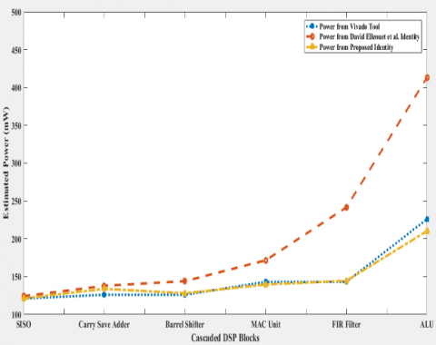
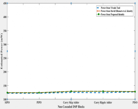
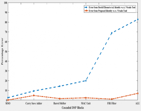
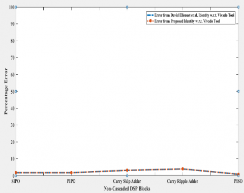
Analysis for various DSP blocks has been carried out at 125 MHz frequency. The comparison results for cascaded and non- cascaded DSP blocks with reference to commercial tool have been shown in Figure 3 and Figure 4 respectively. From the results obtained it has been analyzed that the model proposed by Elleouet et al. [3] is working reasonably accurate for non-cascaded blocks. The maximum error obtained for complex non-cascaded blocks such as carry ripple adder is 3.96% as shown in Figure 6. But the percentage error is very large for cascading blocks with more complexity such as FIR filter, ALU, MAC unit, barrel shifter etc. For SISO cascading block, the percentage error obtained using Elleouet et al. [3] identity is 2.52% as its architecture is fairly simple. It consists of only D flip-flop IPs. However, the error is reduced to 0.08% using proposed identity.
Figure 3. Power analysis of cascaded DSP blocks
Figure 4. Power analysis of non-cascaded DSP blocks
Figure 5. Error analysis of cascaded DSP blocks
Figure 6. Error analysis of non-cascaded DSP blocks
The error obtained for complex cascading circuits with reference to the power values from the commercial tool indicates that the identity proposed by Elleouet et al. [3] is providing inaccurate results particularly for cascaded systems. But, when the power is calculated for cascaded systems using the proposed identity, the error obtained against commercial tool is very low. The maximum error obtained for fairly complex circuit i.e., ALU is only 6.97%. The graph of error for cascading DSP blocks shown in Figure 5 indicates that the proposed identity based on IP modeling is accurately measuring the power for cascaded DSP blocks. Since the proposed identity in this work is same as Elleouet et al. [3] identity for non-cascading DSP blocks, the error values obtained for non-cascading DSP blocks using proposed identity is same as obtained using Elleouet et al. [3] identity.
Accurate power estimation at the early design cycle is the major need today. For complex systems it may take 40-45min to get the power values. Therefore, in the proposed work, power models of the individual IP core are created based on the post synthesis data only. Thus, adopting this methodology for power model creation will save the design implementation time. Also, once the models are created for individual IP cores, these models can be utilized to approximate the power of such systems that are constructed using these IP cores.
The proposed power estimation methodology estimates the total power of a complete system consisting of required number of IPs based on the power values estimated using the power models of the individual IPs. Hence, the power of complete system based on IP modeling can be approximated quickly and accurately without using the commercial tool, based on the knowledge of individual IP cores used in designing a particular system. So, with this approach, design efficiency can be enhanced, also, this will help designer to design any power efficient systems quickly.
To showcase this, a comparison of execution time of complete system using the commercial tool (Vivado) and using proposed methodology is reported in Table 11. The time commercial tool takes to generate the power of any design is the design execution time. For determining the execution time of system using proposed methodology tic-toc MATLAB function has been used. The models are implemented in MATLAB R2013a environment with Windows 64-bit OS + processor Intel Core i5 ~ 3.6 GHz. Variation in time value may occur for different hardware, OS and programming languages.
From the time values reported in Table 11 it can be said that the proposed methodology estimates the total power of a system in fraction of seconds while the commercial tool takes more than 1 minute for estimating the total power. This difference is for simple design but for complex designs it may be very large.
Table 11. Comparison of execution time for different systems
|
IP based system |
Design execution time using commercial tool |
Elapsed time using MATLAB |
|
SIPO |
01 min 26 s |
1.5 ms |
|
PIPO |
02 min 22 s |
1.6 ms |
|
Carry Skip Adder |
01 min 42 s |
1.67 ms |
|
Carry Ripple Adder |
02 min 13 s |
2.09 ms. |
|
PISO |
01min51 s |
1.79 ms |
|
Carry Save Adder |
01min 36 s |
1.47 ms |
|
Barrel Shifter |
01min 57 s |
3.3 ms |
|
ALU |
02 min16 s |
3.2 ms |
|
FIR |
01 min 37s |
1.2 ms |
|
MAC |
01 min 56 s |
3.1 ms |
|
SISO |
01 min 43 s |
1.4 ms |
|
Test Designs |
||
|
QPSK |
6 min 43sec |
3.8 ms |
|
BPSK |
4 min 53 sec |
3.1 ms |
Table 12. Comparative analysis at different frequencies
|
Frequency (MHz) |
Multiplier configuration |
Dynamic power (mW) from tool |
Dynamic power from model (mW) |
Total power from Vivado |
Total power from proposed model |
%Error |
|
125 |
8X8 |
19 |
17.79 |
139 |
137.79 |
0.87 |
|
250 |
8X8 |
37 |
35.58 |
157 |
155.58 |
0.91 |
|
375 |
8X8 |
55 |
53.37 |
175 |
173.37 |
0.93 |
|
500 |
8X8 |
75 |
71.16 |
195 |
191.16 |
1.96 |
The curve-fitting and regression-based model proposed in this work for individual IP cores is generalized for all frequencies as depicted in Table 12. The resource utilization would remain the same for all frequencies. Since the model proposed for individual IP cores is based on resource utilization it will work accurately for all frequencies. The dynamic power will vary in direct proportion with the frequency. For instance, if at frequency f1 the dynamic power is p1, then at frequency a*f1 the dynamic power would be a*p1. Thus, if we double the frequency, the power will also get double. From the result obtained for multiplier IP core for 8x8 configuration at different frequencies it can conclude that the power at each frequency can be obtained by just multiplying the dynamic power with the scaling factor (i.e. The factor by which frequency is scaled). It can also be concluded from the % error obtained at different frequencies that the proposed model is producing highly accurate results at higher frequencies. Thus, with the proposed methodology total power can be approximated quickly and accurately at different frequencies.
In this work, different DSP blocks have been analyzed for power. Blocks have been categorized as cascaded and non-cascaded blocks. After analyzing the results obtained for various DSP blocks, it can be concluded that the power obtained using Eq. (41) is inaccurate particularly for complex cascading systems. However, model works fairly accurate for non-cascading circuits. The maximum error obtained for cascading circuits is 82.84%, which is very large. This realism indicates that the identity projected by Elleouet et al. [3] needs reconsideration, particularly for cascading systems. So, we tried to eradicate the indistinctness that exists in the David Elleouet et al. identity. Therefore, in this work, a power estimation identity for complete system designed using an IP modeling approach has been proposed by considering cascaded DSP blocks at RTL level. It has been analyzed from the result obtained that the proposed identity for cascaded systems is accurate in comparison with Elleouet et al. [3] identity. The maximum error obtained using proposed identity for ALU is only 6.97%, which is very low in comparison with the error obtained using Elleouet et al. [3] identity. So, based on the results obtained we can say that the proposed identity is generic for cascaded and non- cascaded DSP systems and will have a broader spectrum for other systems as well.
This research did not receive any specific grant from funding agencies in the public, commercial, or not-for-profit sectors. The authors would like to thank the editor and anonymous reviewers for their comments that help improve the quality of this work.
[1] Kuon, I., Rose, J. (2007). Measuring the gap between FPGAs and ASICs. IEEE Transactions on Computer-Aided Design of Integrated Circuits and Systems, 26(2): 203-215. https://doi.org/10.1109/TCAD.2006.884574
[2] Mars, S., El Mourabit, A., Moussa, A., Asrih, Z., El Hajjouji, I. (2016). High-level performance estimation of image processing design using FPGA. In 2016 International Conference on Electrical and Information Technologies (ICEIT), pp. 543-546. https://doi.org/10.1109/EITech.2016.751969
[3] Elléouet, D., Julien, N., Houzet, D. (2006). A high level soc power estimation based on IP modeling. In Proceedings 20th IEEE International Parallel & Distributed Processing Symposium, pp. 5-29. https://doi.org/10.1109/IPDPS.2006.1639468
[4] Jevtic, R., Carreras, C. (2009). Power estimation of embedded multiplier blocks in FPGAs. IEEE Transactions on Very Large-Scale Integration (VLSI) Systems, 18(5): 835-839. https://doi.org/10.1109/TVLSI.2009.2015326
[5] Lorandel, J., Prévotet, J.C., Hélard, M. (2016). Fast power and performance evaluation of FPGA-based wireless communication systems. IEEE Access, 4: 2005-2018. https://doi.org/10.1109/ACCESS.2016.2559781
[6] Deng, L., Sobhti, K., Zhang, Y., Chakrabarti, C. (2011). Accurate models for estimating area time and power of FPGAs implementations. In Signal Processing Systems, 63: 39-50.
[7] Gebotys, C.H., Gebotys, R.J. (1999). Statistically based prediction of power dissipation for complex embedded DSP processors. Microprocessors and Microsystems, 23(3): 135-144. https://doi.org/10.1016/S0141-9331(99)00030-7
[8] Verma, G., Dabas, C., Goel, A., Kumar, M., Khare, V. (2017). Clustering based power optimization of digital circuits for FPGAs. Journal of Information and Optimization Sciences, 38(6): 1029-1037. https://doi.org/10.1080/02522667.2017.1372154
[9] Nasser, Y., Lorandel, J., Prévotet, J.C., Hélard, M. (2020). RTL to transistor level power modeling and estimation techniques for FPGA and ASIC: A survey. IEEE Transactions on Computer-Aided Design of Integrated Circuits and Systems, 40(3): 479-493. https://doi.org/10.1109/TCAD.2020.3003276
[10] Raghunathan, A., Dey, S., Jha, N.K. (1996). Register-transfer level estimation techniques for switching activity and power consumption. Proceedings of International Conference on Computer Aided Design, 96: 158-165. https://doi.org/10.1109/ICCAD.1996.569539
[11] Makani, M., Niar, S., Baklouti, M., Abid, M. (2018). HAPE: A high-level area-power estimation framework for FPGA-based accelerators. Microprocessors and Microsystems, 63: 11-27. https://doi.org/10.1016/j.micpro.2018.08.004
[12] Durrani, Y.A., Riesgo, T. (2014). Power estimation for intellectual property-based digital systems at the architectural level. Journal of King Saud University-Computer and Information Sciences, 26(3): 287-295. https://doi.org/10.1016/j.jksuci.2014.03.005
[13] Singh, N., Verma, G., Khare, V. (2022). Power Estimation and Validation of Embedded Multiplier Based on ANN and Regression Technique. Journal of Circuits, Systems and Computers, 31(5): 2250086. https://doi.org/10.1142/S0218126622500864
[14] Singh, N., Verma, G., Khare, V. (2020). Power estimation of FIR filter based on IP modeling for DSP and communication applications. In 2020 Global Conference on Wireless and Optical Technologies (GCWOT), pp. 1-7. https://doi.org/10.1109/GCWOT49901.2020.9391608
[15] Landman, P. (1996). High-level power estimation. In Proceedings of 1996 International Symposium on Low Power Electronics and Design, pp. 29-35. https://doi.org/10.1109/LPE.1996.542726
[16] Julien, N., Laurent, J., Senn, E., Martin, E. (2003). Power consumption modeling and characterization of the TI C6201. IEEE Micro, 23(5): 40-49. https://doi.org/10.1109/MM.2003.1240211
[17] Xilinx power estimator. http://www.xilinx.com/products/technology/power/xpe.html, accessed on 10 June 2022.
[18] Verma, G., Kumar, M., Khare, V., Pandey, B. (2017). Analysis of low power consumption techniques on FPGA for wireless devices. Wireless Personal Communications, 95(2): 353-364.
[19] https://www.allaboutcircuits.com, accessed on 10 June 2022.
[20] Laurent, J., Julien, N., Senn, E., Martin, E. (2004). Functional level power analysis: An efficient approach for modeling the power consumption of complex processors. In Proceedings Design, Automation and Test in Europe Conference and Exhibition, 1: 666-667. https://doi.org/10.1109/DATE.2004.1268921
[21] Verma, G., Kumar, M., Khare, V. (2017). Low power synthesis and validation of an embedded multiplier for FPGA based wireless communication systems. Wireless Personal Communications, 95(2): 365-373. https://doi.org/10.1007/s11277-016-3897-1
[22] MATLAB. http:// www.mathworks.com, accessed on 10 June 2022.