Guillaume Pellecuer* | Jean-Jacques Huselstein | Thierry Martiré | François Forest | André Chrysochoos | Mourad Jebli
© 2022 IIETA. This article is published by IIETA and is licensed under the CC BY 4.0 license (http://creativecommons.org/licenses/by/4.0/).
OPEN ACCESS
Wirebonds ageing in power modules used in electric vehicles is a main concern for the development of reliable inverters. The development of a specific test bench to study the evolution of their properties over time has allowed conclusions to be drawn on the possibility of accelerating or not accelerating ageing tests without distorting the mechanisms actually involved in ageing. Through the use of specifically developed test bench in terms of electrical and thermal properties the studied wirebonds samples are more easily thermally controllable, equipped with measuring devices and the energy consumption at a given cycle is divided by ten compared to a classical bench. The entire process of designing and producing the specific samples and the associated test bench and a description of the first results obtained to demonstrate the relevance of the approach is given.
wirebonds ageing, power cycling, specific samples design, test benches development
The power semiconductor modules are key elements in the structure of a converter and their reliability has a strong influence on the reliability of the whole system. In the case of electric traction applications, the thermal environment or the power losses in the semiconductor chips lead to so-called passive or active thermal cycling. This phenomenon is one of the main causes of ageing and degradation of these components, especially in the upper connections called wirebonds [1, 2].
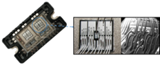
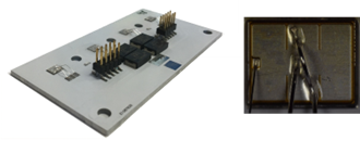
The chips used in this context are mainly integrated into power modules (Figure 1) to constitute elementary conversion functions. This assembly must be able to maintain electrical insulation of the active parts and ensure the mechanical support of the different elements of the structure. The result is a multi-layer stack of different materials that are sensitive to thermal cycling. The different layers have significant differences in terms of thermo-mechanical properties, leading to the development of large mechanical stress fields at the interfaces and especially at the upper connections, known as wirebonds. Under these conditions, the reliability of the modules is directly related to thermo-mechanical fatigue of wirebonds [3, 4].
Figure 1. Power module with wirebond view
To study the ageing of connections in power modules, test benches were used. IES-GEM (Institut d’Electonique et des Systèmes - Groupe Energie et Materiaux) has developed a PWM test bench that can actively cycle (Figure 2) the component [5-7]. It allows ageing tests to be carried out on modules by applying electro-thermal stresses like those experienced by these components in real operation and the structure of the converter is a single-phase PWM (Pulse Width Modulation) inverter with two arms operating in opposition. This converter structure has the advantage of being able to apply realistic operating conditions while drawing only the losses of the active components (IGBT (Insulate Gate Bipolar Transistor), diodes) on the power supply [6, 8]. Each test bench allows two generic modules (two IGBTs and two diodes) to be tested.
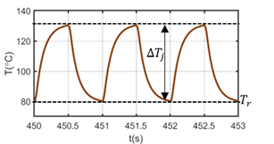
Figure 2. Thermal cycles of IGBT chip
The use of PWM test benches has many advantages, such as ageing under realistic conditions. However, the implementation of PWM test benches is tedious, time consuming, energy consuming and it is very difficult to perform on-line measurements like $V_{C E}$ monitoring for example [9]. Moreover, as the objective is to focus on the top part of the chip with its connections, the use of commercial power modules as a test sample is not the simplest solution. The entire assembly must be stressed in order to observe only a small part of it, and the large number of bondings on each chip does not allow the behaviour of a single wire to be correctly characterized.
The idea developed here is therefore to create test samples dedicated to the study of connections, with low power consumption and with the possibility of carrying out on-line measurements characterizing the state of damage of the fastener. The ageing of the bonding wires associated with such samples will have to be similar to that caused by conventional tests, consequently the stresses applied to the wires and their attachments will have to be maintained. Some twenty samples were manufactured and tested to validate the approach from design to production of such samples and the operation of the ageing benches.
2.1 Using a IMS
The basic principle of our approach has consisted in using a thermally "bad" substrate in order to generate thermal cycling much more easily. For this purpose, we have chosen an IMS (Insulated Metal Substrate) with an epoxy insulating layer, on which MOSFET (Metal Oxide Semiconductor Field Effect Transistor) chips were soldered and used as heat sources in linear mode. The Drain-Source voltage is imposed by the power supply and a current control allows to generate a power cycling. In addition the device was placed on a heat sink with controlled air flow. This IMS presents a high thermal resistance between the lower and upper metallizations, allowing a considerable reduction in power consumption compared to the PWM bench, for a given thermal cycling of the chips $(55 \mathrm{~W}$ instead of $400 \mathrm{~W}$ as in the previous PWM test bench [10], for a sample with four chips compared to one module, for $T_j=50 \mathrm{C}, T_r=80^{\circ} \mathrm{C}$ and $f=1 \mathrm{~Hz}$ ) [11]. We have taken $1 \mathrm{~Hz}$ as the cycling frequency to illustrate the operation of the bench as this is a frequency commonly encountered in the accelerated cycling of wirebonds in semi-conductor power modules.
IMS assembly:
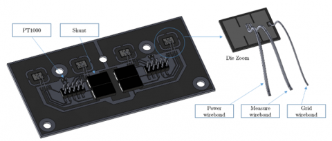
Figure 3. 3D view of an IMS sample
Figure 3 shows a 3D view of a sample drawn with SOLIDWORKS®. The test sample consists of four MOSFET chips each with three bonding wires:
A shunt, associated with each chip, allows the main current to be measured and regulated. Since the system operates in linear mode with a constant $V_{D S}$ voltage, the current regulation allows the losses in the chip to be perfectly controlled. Unlike the PWM test bench, in which the losses depend on the chip (conduction and switching) and therefore have a dispersion, the losses here are identical for all chips. Two temperature measurements are made using PT1000 type platinum probes on the top of the IMS. These two measurements are considered here as the $T_{\text {ref }}$ reference temperature for imposing thermal cycling. Two connectors are used to connect the drivers board to the power board, the regulation and measurement conditioning circuits are also located on the drivers board.
2.2 Electrothermal modelisation
The feasibility of this solution was verified by electrothermal finite element simulations on COMSOL Multiphysics® software.
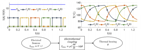
Figure 4. 1Hz cycling simulation example (*)
*For the sake of visibility, the currents on the left-hand side of the figure above does not correspond to the real currents injected to obtain the thermal profiles on the right-hand side (Actual: Dt = 0.5, Imax = 1.8A, I0 = 0.5A).
The concept of enforcing a constant voltage and regulating the drain current of the MOSFET to control the heat source can be implemented in the circuit simulator included in the finite element software. A voltage condition is imposed (Potential and Ground) and a time-varying chip electrical conductivity is calculated to obtain the desired current. Figure 4 shows an example of a simulation with four alternating currents in the chips and the resulting thermal profiles, for a cycling frequency of 1Hz.
As the sample is intended to be mounted on a finned heat sink, a forced convection thermal condition is applied to the fins. Figure 5 shows an example of a simulated thermal mapping during alternate cycling of the four chips. Isthmuses in the conductive copper layer are visible around the chips and allow each MOSFET to be considered as thermally isolated because for low frequencies, it is necessary to limit the propagation of heat so that the cycling of one chip does not impact the cycling of its neighbours. There are two possible solutions to overcome this problem: to separate the chips by large spaces or to make these isthmuses. The latter solution has the advantage of increasing the number of chips per substrate. The isthmuses must considerably increase the thermal resistance between chips linked to the conductive layer while presenting a sufficiently low electrical resistance. Simulations have shown local current densities of 15A/mm2 in the copper for the currents which is quite acceptable.
Figure 5. Heat map of the sample
These simulations also validated the feasibility of cycling at $0.1 \mathrm{~Hz}, 1 \mathrm{~Hz}$ and $5 \mathrm{~Hz}$ with temperature profiles $T_j=50^{\circ} \mathrm{C}$ and $T_r=80^{\circ} \mathrm{C}$, to reproduce test conditions similar to those applied to power modules (to allow the comparison). The chips are exposed to the same thermal profile, but a phase shift between them is deliberately introduced. This allows the currents to be balanced and thus limits the ripple of the current seen by the power supply.
2.3 Making samples
Figure 6. Substrat IMS – chip zoom
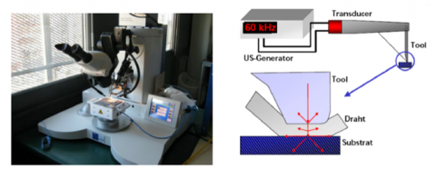
Figure 6 shows the resulting substrate and a closer look at one of the chips. The components (shunts, PT1000, chips, copper pads and connectors) are soldered using a tin-lead solder. The bonding wire connections are the main focus of the study. It is therefore interesting to take a closer look at the transferring technique of these wires. This step is carried out using a "Heavy Wire Bonder HB30" machine, available within the 3DPHI platform (Figure 7).
Figure 7. Heavy wire bonder HB30
The procedure consists of positioning the wire with a tool onto the pad where it is to be welded. The combination of a force applied to the wire during plating and mechanical vibrations created by a transducer allows the welding to be performed. The applied force is adjustable, as well as the application time and the welding power (amplitude/frequency of the ultrasonic waves). The dissipated energy causes the wire to soften in a similar way to that obtained by raising the temperature. The wire is then guided to a second pad to make a new weld. A knife is used to cut the wire once the bond has been made [12, 13]. The wire diameter used for our samples is 250μm for power and measurement while a wirebond with a 125μm diameter is used for the grid wirebond.
Figure 8. Configuration of bonding placement
The transfer of bonding wires can be done with or without emitter repetition (two legs, or one leg, Figure 8). The study of these two configurations will make it possible to analyse the possible influence of the stresses developed in one bonding foot on the second foot and to evaluate the impact on ageing. The welding parameters are identical to those used by power module manufacturers. Power: 6W - Time: 150ms - Force: 450mN.
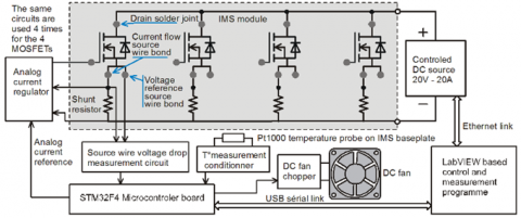
A test bench for electrothermal cycling of the samples has been developed, its synoptic diagram is given in Figure 9.
Figure 9. Schematic diagram of the test bench
The shaded area in Figure 9 is the test sample. The other blocks correspond to the driving and control functions implemented in the test bench. The control system is implemented in a STM32F4 microcontroller from STMicroelectronics® which controls the current for the four channels using four PWMs. The LabVIEW® supervision interface allows, via the microcontroller UART (Universal Asynchronous Receiver / Transmitter), the monitoring of current measurements, contact resistance measurements and temperatures for regulation. Moreover, the power parameters can also be adjusted via the control of the input current from the user. A temperature regulation based on the control of the air flow in the fins via a buck converter/fan assembly is implemented in the STM32F4. The STM32F4 also counts and saves the number of cycles on each channel. In addition, the LabVIEW® interface also makes a backup. The supervisory interface also allows the voltage and current of the main power supply to be monitored via Ethernet communication and the information on the current drawn to be used to detect a short-circuit fault and shut down the power supply. Contact resistance measurements, taken by the microcontroller, are stored in a file. A MATLAB® "App designer" interface allows to read this file, to filter the measurements (sliding average) and to display the results as curves. This interface allows to follow the evolution of the contact resistance in real time.
The test bench is designed to allow the variation of many cycling parameters such as frequency $f$, current amplitude $I_{\max }$ and $I_0$, duty cycle $D_t$, supply voltage $U_E$ and reference temperature of the cycle $T_{\text {ref }}$.
Variation ranges:
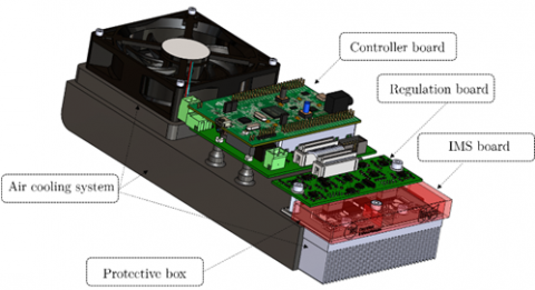
Figure 10. 3D Implementation of the test bench
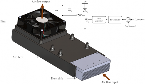
Figure 10 shows an overview of the test bench designed using Solidworks®. This includes the IMS board, which is described in detail in the previous section. The driver board, which contains the measurement and control circuits for the four sample channels is plugged into the driver board via two 10-pin connectors. A support PCB (controller board) houses the microcontroller board and provides the interface between the monitoring tool and the driver board. The buck converter used to control the variable speed fan is located on the latter board.
The cooling system consists of a fan, an air box and a finned heat sink to which the IMS board is attached. The air box also serves as a support for the controller board.
Finally, a protective casing is fitted to the IMS board to prevent damage of the bonding wires during the various steps of board assembly and disassembly.
3.1 Principle of power control and measurement
In order to impose the chip temperature variations via their losses, the choice was made to regulate the drain current with a constant $V_{D S}$ voltage (neglecting the shunt voltage). This regulation is analog (driver board), its schematic diagram is shown in Figure 11.
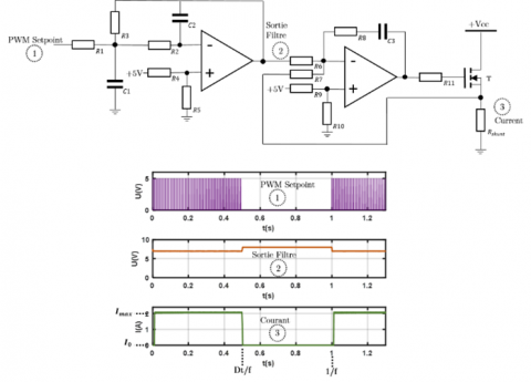
Figure 11. Schematic diagram of the current control
The current set point, generated by the microcontroller, is imposed by a high-frequency PWM signal whose duty cycle, which is an image of the set point, is variable in time. A low-pass filter is used to extract the low frequency component of the signal that has the desired current shape. The current measurement is carried out using a 0.2W shunt. A proportional integral PI (Propotionnal, Integral) controller is inserted into the loop and directly controls the MOSFET through a gate resistor (Figure 12).
Figure 12. Analog control of drain current
In Figure 12, control signal 1 is the PWM set point from the microcontroller board. Signal 2 is the filtered signal. To avoid using a symmetrical power supply, an offset is added to each operational amplifier. The $8 \mathrm{~V}$ level appearing at the output of the filter is caused by this offset. It is then compensated by the offset of the PI controller. Signal 3 is the controlled current. The setting parameters are the frequency $f$, the low frequency duty cycle $D_t$, the amplitude $I_{\max }$ and the low value $I_0$.
The driver board also contains the conditioning circuits for all the measurements. The data from these circuits is then sent to the microcontroller board via the analog/digital conversion inputs.
Eleven measurements are made on each sample:
The controller board is the main element of the bench. It includes the various power supplies required for the operation of the test bench, the fan buck converter and supports the microcontroller board.
3.2 Air cooling system
To control the thermal profile of a chip, a power profile must be imposed, but also the "low" temperature of the profile called $T_r$ (Figure 2). This ensures reproducible thermal behaviour. For this purpose, the $T_{\text {ref }}$ temperature, measured using two PT1000 platinum probes placed on the IMS board, is digitally controlled. For the considered cycling frequencies, the $T_{r e f}$ and $T_r$ temperatures are directly proportional to each other.
The system (Figure 13) consists of a heat sink with the sample screwed to it, a fan operating at variable speed for thermal regulation and an air box for airflow ducting. The measurements from the PT1000 are conditioned by a circuit on the driver board and an equation resulting from the polynomial interpolation of the sensor conditioning circuit response set in the supervisory interface, is used to obtain the temperature. The measurement of the reference temperature corresponds to the average of the two measurements made by the probes.
Figure 13. 3D view of the air cooling system
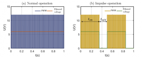
A buck converter allows the control of the fan. The adjustment of its speed allows the control of the temperature measured on the IMS board. The fan works in air extraction mode. As the heat flow to be extracted is low, holes are provided at the back of the box to increase the air flow drawn in by the fan and thus facilitate the control. The fan does not have a linear speed/voltage characteristic and below a voltage threshold, and therefore speed, the fan stops. In order to be able to impose speeds below this threshold, the duty cycle is set to its minimum value and an ON/OFF modulation is introduced, with a period less than the mechanical time constant of the fan motor. The pseudo duty cycle $t_{O N} / t_{O F F}$ is controlled by the supervisory interface which sends the two orders (PWM and $t_{O N} / t_{O F F}$ ) to the microcontroller which generates the PWM.
Figure 14. Two modes of fan control
The two fan operation modes are shown in Figure 14. The control mode above the limit speed, is as shown in Figure 14 (a) and below the limit speed, the control mode is the one shown in Figure 14 (b). The transition between the two modes is linear. This means that once the minimum HF (high frequency) duty cycle is reached for normal operation, the LF (low frequency) duty cycle is gradually reduced to slow down the fan and to comply with the control commands. The frequency of the ON/OFF modulation is set to 2Hz, whereas the value of the switching frequency which is 100kHz. Therefore, the buck converter filter has no influence on the low frequency modulation.
The air box was produced by 3D printing (PRO3D® additive manufacturing process technology platform of the University of Montpellier). The material used is ABS plastic which can withstand temperatures above 100°C. Under normal bench operating conditions, the maximum temperature to which the air box can be subjected is approximately 80°C. The protective casing was also manufactured by 3D printing.
3.3 Live contact resistance measurement
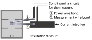
The objective being to have feedback on the ageing of the contact area, we chose to carry out a live electrical resistance measurement [14]. The second bonding wire in Figure 15 was provided for this purpose. It is used to measure the voltage drop across the power bonding wire at a given current. The resistances thus measured include that of the wire, its attachment to the chip and an active part of the metallization between the two attachments. In the event that only the contact area degrades, the detected change in resistance would be the marker.
Figure 15. Schematic of contact resistance measurement
Figure 15 shows the wiring geometry chosen to make this measurement. The voltage drop across the bonding wire is small and difficult to measure with the currents flowing through the chips (1 to 2A). Indeed, the resistance of the wires is about 10mΩ, which leads to voltages of 10 to 20mV. Furthermore, the measurement must be reproducible, and the resistivity of aluminium is temperature dependent. The measurement cannot therefore be made during cycling and must be carried out during a sequence of measurements which interrupts the cycling.
During this measurement sequence, the voltage generated by the power source is lowered to the minimum possible (3V instead of $12 \mathrm{~V}$ ) and a current of 5A is imposed in each chip (leading to a voltage drop of about 50mV) for a very short time (20ms), in order to avoid a temperature rise of the chip. Considering the low energy dissipated during this measurement and the low thermal capacity of the chip-soldercopper assembly, the junction temperature $T_j$ varies only slightly during the measurement and is equal to the regulated temperature $T_{\text {ref }}$. The measurement is performed every three hundred cycles for each channel. The supervisory interface starts the measurement sequence by sending the corresponding voltage set point to the controllable power supply and informs the microcontroller, which in turn imposes a DC current in each channel to discharge the output capacitors of the power supply and then generates the current set points, channel by channel, to obtain the current of 5A for 20ms.
Acquisitions are made at 1kHz on the relevant analogue/digital conversion inputs and can store fifteen pairs of voltage drop and current value. The result is sent to the LabVIEW® interface for resistance calculation (the fifteen values are averaged to have a reliable measurement) which is then stored in a text file for the cycling follow-up. After each measurement, the number of cycles is stored in the flash memory of the microcontroller to save the information in case of power failure. The measurement does not require extreme accuracy, but it must be able to detect a change in contact resistance at the plating-bonding interface. It is the relative change in resistance that is meaningful in relation to the progressive degradation of the wirebond.
3.4 Supervisory interfaces
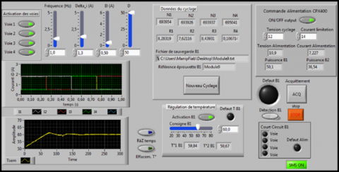
The main supervision interface is implemented with LabVIEW® software. It allows to impose and adjust the cycling parameters (for current and temperature control) and to visualise the currents in the chips as well as the temperature measured by the platinum probes or cycling information (number of cycles and resistance measurements). Figure 16 shows a view of the supervision window.
Figure 16. Half LabVIEW® supervisory interface (*)
* For the sake of visibility, only half of the supervisory interface is shown, allowing a single test bench to be controlled. The interface allows two benches to be controlled independently in the same way.
The supervisory interface controls two benches with a controlled voltage source for their power supply. In the middle of the control window are the source control parameters and short-circuit fault indicators. The microcontroller monitors the current of each channel for each bench, while the overall monitoring of the power supply current is done by the LabVIEW® application. In the event of a problem, the power supply is automatically switched off. The current drawn by the two benches, as well as the voltage and power drawn by each bench are also displayed.
A second interface, for the real-time display of resistance measurements, was created using the MATLAB® tool "Appdesigner" (Figure 17). The use of MATLAB® signal processing tools allows for flexibility in the processing of data from resistance measurements.
It allows the variation of the wire resistance to be displayed for the four benches that have been manufactured. For the display, a sliding average is taken over the last one hundred measured values. The resistance value, thus obtained, is compared with the average of the first one hundred measurements. From this, the resistance change (in %) is calculated, and this is the value displayed on the graphs.
Figure 17. Matlab®supervisory interface
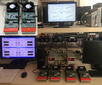
Four test benches with one IMS per bench were built to test four IMS samples corresponding to sixteen bonding wires. Several types of samples were made during four test campaigns, depending on the information gathered during the tests. Figure 18 shows an overview of the bond wire ageing platform.
Figure 18. Test platform for ageing of samples
The platform, which comprises four test benches, is operational and has made it possible to test some twenty IMS samples corresponding to eighty wirebonds, in three measurement campaigns, under cycling conditions that will be detailed in the following section. A thermal camera is also used at the beginning of each cycle to check the thermal profile.
4.1 Example of 1Hz power cycling protocol
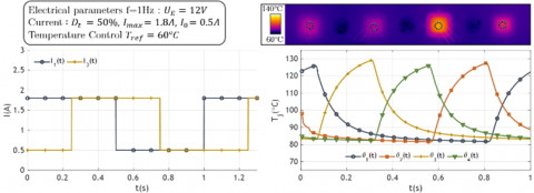
The first objective is to verify the representativeness of the samples thus produced. To do this, we decided to carry out several ageing campaigns, with a cycling frequency of 1Hz and a chip temperature $T_j$ varying between 80°C and 130°C.
The cycling parameters are selected as follows:
All the results presented here were obtained with these thermal cycling parameters (Figure 19). Only the currents flowing in chips 1 and 3 are shown on the left-hand graph for visibility reasons. Using the infrared thermal camera, the electrical parameters to be applied to obtain the desired thermal profile were determined. These parameters are shown on the graph representing the currents. The calculation (Eq. (1)), with Figure 19 parameters, gives an average power consumption of 55.2W for one IMS (four chips), it is important to remember that the benches previously used [10] consumed nearly 400W for the same work.
$P=4 \times U_E \times\left(D_t \times I_{\max }+\left(1-D_t\right) \times I_0\right)$ (1)
Figure 19. 1Hz cycling protocol
For the temperature measurement, each circle visible on the heat map in Figure 19 defines an integration area on the chip. The result is the average of all the temperatures measured on each pixel present in the circle. The few thermal imbalances observed on the graphs are probably due, on the one hand, to the uncertainty of the observation areas used for the measurements and, on the other hand, to differences in the quality of the welds.
Not all modules can be observed with a thermal infrared camera and we considered this thermal profile to be reproducible at fixed electrical test conditions.
4.2 Test results for 1Hz power cycling protocol
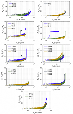
The 1Hz cycling protocol was applied to about twenty IMS samples, i.e. about eighty chip-bonding pairs were tested. The objective was to validate the proper working of the test benches and to analyse the relevance of an electrical measurement to characterise mechanical damage. For these different samples, many parameters were analysed such as the effect of an emitter repetition or the impact of the silicone gel... A comparison was made between welds made by a manual machine and an automatic machine. Indeed, some samples were soldered by the MICROCHIP® company (ex MICROSEMI®), which has a perfect knowledge of power module soldering techniques. Figure 20 shows examples of the obtained results.
$R_b$ is the resistance value after $N_f$ cycle and $R_{b 0}$ the resistance value at the beginning of life. The curves represent the contact resistance measurement show a progressive increase in resistance. This increase becomes very significant at the end of the life cycle where a thermal runaway occurs due to poor current distribution in the connection, thus creating local heat sources that accelerate the destruction of the connection. These graphs show some trends in the fatigue of power modules by showing a clear dependence of the variation of the electrical resistance of the wire on the damage. Lemaitre and Chaboche defined a damage D relative to the current variation [15] (Eq. (2)).
$\tilde{i}=\frac{i}{1-D}$ (2)
Figure 20. Evolution of contact resistance
$\tilde{i}$ being the current variation after $N_f$ cycle and $i$ the current at $N_f=0$. This equation is only valid if one considers that the damage only influences the current density and that the resistance variations are only due to geometrical changes due to elastic and plastic deformations. Here, it is considered that the damage has an influence on the resistance via the degradation of the contact interface with:
$D=\frac{S}{S_D}$ and $R=\rho \frac{L}{S}$ (3)
$S_D$ is the damaged area, $S$ the total area, $R$ the resistance, $\rho$ the electrical resistivity, $L$ and $S$ are the length and the area of the contact. Finally, the damage can be written as:
$D=\frac{R_b-R_{b 0}}{R_b}$ (4)
The evolution of resistance $\left(R_b-R_{b 0}\right) / R_b$, shows a trend that would confirm this equation justifying the relevance of this type of measure. Each sample was analysed by SEM (scanning electron microscopy) to assess the failure modes. Two failure modes were observed, namely metallization degradation and bond wire lift off. Figure 21 shows the top of a chip before and after ageing.
Figure 21. SEM failure analysis of wirebonds
These tests are encouraging, but the results obtained on the bonding wires of these samples are far from those observed on industrial modules with longer lifetimes. The use of MOSFET chips with a much larger semiconductor chip and solder thickness than an IGBT module partly explains this difference [16]. The objective of this study is therefore to set up test benches capable of highlighting the thermomechanical mechanisms responsible for the ageing of wirebonds. From this point of view, the test bench described here perfectly meets the expectations in terms of facilitating the management of thermal cycles and the ability to perform measurements in real-time.
The results obtained with this tool perfectly reflect the thermomechanical mechanisms responsible for the ageing of the connections. Indeed, the resistance variation remains during a large number of cycles during the implementation of the visco plasticity cycle characteristic of these connections. Thermomechanical modelling work shows significant viscoplastic deformations of the bond wires from the beginning of the loading, trending towards a stabilised cycle. This small but real increase in plastic deformation during each cycle suggests damage to these connections. This progressive damage finally creates a thermal runaway due to the distribution of the current density in the bonding foot zone which progressively reduces with increasing damage. This thermal runaway, which accelerates the lift-off of the wires can be seen very clearly on the curves in Figure 20 [3, 17].
There are several positive aspects to note, such as the possibility of producing specific samples with limited resources, the minimization of power consumption or the possibility to precisely control the test conditions. In addition, many benches can be run in parallel, allowing tests to be carried out over a period of weeks and a large amount of data to be collected. The implementation of the measurement monitoring (in this case, contact resistances) is relatively easy and can take a number of different forms, as specific samples can be designed at wish. Although they do not fully meet our expectations compared to data collected with industrial modules, these tests indicate a good reproducibility of applied thermal stresses and ageing modes, both in nature and in time evolution.
We have proposed the creation of specific test samples as well as all the necessary steps for their realisation and the creation of the associated test bench. We have chosen to measure the resistance of the bonding in order to evaluate in real time the evolution of the damage of the connection. The first results suggest that such a measurement is a good option for analysing bonding wires fatigue. However, these samples are only of interest if they can accurately represent, from the viewpoint of ageing, the bonding technology found on commercial modules. The curves, obtained over a campaign of twenty IMS samples, have enriched a study on the modelling of the thermomechanical mechanisms responsible for the ageing of wirebonds and show the interest of the approach presented in terms of ease of control of the cycling parameters as well as the robustness of the real-time measurements of the mechanical damage state. These curves are important for future research work on the development of numerical damage laws using the cohesive zone technique in order to establish, numerically, a representative model in terms of the ageing mechanism of the connections. From this point of view, the test bench thus created meets expectations. However, as one would expect, longer lifetimes are observed than those obtained on conventional modules, for similar thermal cycling. This difference can be explained by the use of thicker MOSFET chips, which limit the mechanical stresses in the attachment area. However, the objective here was not to analyse the representativeness in terms of lifetime, but to validate the interest of the test bench and the relevance of the observed quantities to highlight the failure mechanisms. From this point of view, the interest of this approach remains. The simplicity of implementation, the easiness of measuring the various quantities (voltage, current, temperature, resistance, etc.), the reproducibility of the stresses applied and the long-term energy savings are all advantages that make this solution attractive.
The authors would like to express their gratitude to the company MICROCHIP® (ex MICROSEMI®) for the donation of the chips and their help with the wiring of various samples.
The authors would also like to express their gratitude to the technological platform of the University of Montpellier PRO3D for the realization of the 3D printing supports.
The authors would also like to express their gratitude to the technology platform 3DPHI for help in making samples.
|
$\mathrm{T}$ |
Temperature in °C |
|
$\mathrm{t}$ |
Time in s |
|
$\Delta T_j$ |
Temperature junction amplitude in °C |
|
$T_r$ |
Low temperature of the temperature cycle in °C |
|
$T_{ref}$ |
Reference temperature for a control in °C |
|
$V_{C E}$ |
Collector-Emitter voltage in V |
|
$\mathrm{f}$ |
Cycling frequency in Hz |
|
$T_j$ |
Junction temperature in °C |
|
$k$ |
Thermal conductivity in W/m.K |
|
$D_t$ |
Low frequency duty cycle |
|
$I_{\max }$ |
Maximum current in A |
|
$I_0$ |
Minimum current in A |
|
$V_{D S}$ |
Drain-Source voltage in V |
|
$V_{G S}$ |
Grid-Source voltage in V |
|
$U_E$ |
Supply voltage in V |
|
$V$ |
Voltage in V |
|
$i$ |
Current in A |
|
$P$ |
Power in W |
|
$\widetilde{i}$ |
Current after $N_f$ cycles |
|
$N_f$ |
Number of cycle |
|
D |
Damage in % |
|
$S$ |
Surface in m2 |
|
$S_D$ |
Damaged surface in m2 |
|
$R_{b 0}$ |
Bonding resistance at $N_f$=0 in Ω |
|
$R_b$ |
Bonding resistance in Ω |
|
$R$ |
Resistance in Ω |
|
$L$ |
Length in m |
[1] Ciappa, M. (2002). Selected failure mechanisms of modern power modules. Microelectron. Reliab., 42: 653‑667. https://doi.org/10.1016/S0026-2714(02)00042-2
[2] Ramminger,S., Türkes, P., Wachutka, G. (1998). Crack mechanism in wire bonding joints. Microelectron. Reliab., 38: 1301‑1305. https://doi.org/10.1016/S0026-2714(98)00141-3
[3] Pellecuer, G., Forest, F., Huselstein, J.J., Martiré, T., Arnould, O., Chrysochoos, A. (2022). Toward a multi-physical approach to connection ageing in power modules. Microelectron. Reliab., 132: 114513. https://doi.org/10.1016/j.microrel.2022.114513
[4] Czerny, B., Lederer, M., Nagl, B., Trnka, A., Khatibi, G., Thoben, M. (2012). Thermo-mechanical analysis of bonding wires in IGBT modules under operating conditions. Microelectron. Reliab., 52(9): 2353-2357. https://doi.org/10.1016/j.microrel.2012.06.081
[5] Smet, V. (2010). Aging and failure modes of IGBT power modules undergoing power cycling in high temperature environments. PhD Thesis. http://www.theses.fr/2010MON20075/document.
[6] Forest, F., Huselstein, J.J., Faucher, S. Elghazouani, M., Ladoux, P., Meynard, T.A., Richardeau, F., Turpin, C. (2006). Use of opposition method in the test of high-power electronic converters. IEEE Trans. Ind. Electron., 53(2): 530‑541. https://doi.org/10.1109/TIE.2006.870711
[7] Forest, F., Rashed, A., Huselstein, J.J., Martire, T., Enrici, P. (2015). Fast power cycling protocols implemented in an automated test bench dedicated to IGBT module ageing. Microelectron. Reliab., 55(1): 81‑92. https://doi.org/10.1016/j.microrel.2014.09.008
[8] Vallon, J. (2003). Introduction à l’étude de la fiabilité des cellules de commutation à IGBT sous fortes contraintes. http://ethesis.inp-toulouse.fr/archive/00000011/.
[9] Smet, V., Forest, F., Huselstein, J.J., Rashed, A., Richardeau, F. (2013). Evaluation of vce monitoring as a real-time method to estimate aging of bond wire-IGBT modules stressed by power cycling. IEEE Trans. Ind. Electron., 60(7): 2760‑2770. https://doi.org/ 10.1109/TIE.2012.2196894
[10] Forest, F., Huselstein, J.J., Pellecuer, G., Bontemps, S. (2017). A Power Cycling Test Bench Dedicated to the Test of Power Modules in a Large Range of Cycling Frequency. In PCIM Europe 2017; International Exhibition and Conference for Power Electronics, Intelligent Motion, Renewable Energy and Energy Management, p. 1‑7.
[11] Gurpinar, E., Ozpineci, B., Chowdhury, S. (2019). Design, analysis and comparison of insulated metal substrates for high power wide-bandgap power modules. ASME 2019 International Technical Conference and Exhibition on Packaging and Integration of Electronic and Photonic Microsystems. https://doi.org/10.1115/IPACK2019-6436
[12] Sedlmair, J., Farassat, F., Schlicht, F. (2012). Which ultrasonic frequency is best for wire-bonding? http://dx.doi.org/10.4071/isom-2011-WA4-Paper2
[13] Fischer, A.C., Korvink, J.G., Roxhed, N., Stemme, G., Wallrabe, U., Niklaus, F. (2013). Unconventional applications of wire bonding create opportunities for microsystem integration. J. Micromechanics Microengineering, 23(8): 083001. http://dx.doi.org/10.1088/0960-1317/23/8/083001
[14] Tang, Y., Wang, B., Chen, M., Liu, B. (2014). Reliability and on-line evaluation of IGBT modules under high temperature. Diangong Jishu XuebaoTransactions China Electrotech. Soc., 29: 17‑23.
[15] Lemaitre, J. Chaboche, J.L. (1990). Mechanics of Solid Materials. Cambridge: Cambridge University Press. https://doi.org/10.1017/CBO9781139167970
[16] Surendar, A., Samavatian, V., Maseleno, A., Ibatova, A.Z., Samavatian, M. (2018). Effect of solder layer thickness on thermo-mechanical reliability of a power electronic system. J. Mater. Sci. Mater. Electron., 29(17). https://link.springer.com/article/10.1007/s10854-018-9667-y.
[17] Pellecuer, G. (2019). Fatigue thermomécanique des connexions dans les modules de puissance à semi-conducteurs. Theses, Université Montpellier. https://tel.archives-ouvertes.fr/tel-02476237.