Yacine Triki | Ali Bechouche | Hamid Seddiki | Djaffar Ould Abdeslam*
© 2021 IIETA. This article is published by IIETA and is licensed under the CC BY 4.0 license (http://creativecommons.org/licenses/by/4.0/).
OPEN ACCESS
This paper proposes a new adaptive orthogonal signal generator (OSG) for a stand-alone single-phase voltage source inverter (VSI) control in synchronous reference frame (SRF). Based on the adaptive linear neuron, the proposed OSG is able to achieve several main tasks. In addition to generating the orthogonal signal, the proposed OSG leads to filtering the original signal and the orthogonal signal; provides directly the direct and quadrature (dq) components in SRF; and identifies the harmonic residue of the output voltage. The harmonic residue compensation in the SRF voltage control scheme leads to improve significantly the output voltage quality. The suggested OSG is experimentally tested and compared with conventional and advanced OSGs. Obtained results are clearly proven its superiority. Thereafter, performances of the suggested SRF voltage control have been evaluated by means of simulations and experiments. Obtained results are shown insignificant steady-state errors and low harmonic distortions in the generated VSI output voltage. Originality of the proposed SRF voltage control lies in the filtering capability of the developed OSG. Therefore, the proposal yields to a simplified SRF voltage control with better performances.
adaptive linear neuron, control in synchronous reference frame, nonlinear load, orthogonal signal generation, voltage source inverter
Electricity production from distributed generation (DG) systems, such as photovoltaic and wind power systems, has grown rapidly these last decades [1]. DG systems, operating in stand-alone mode, have recently gained a lot of attention as a sustainable way for electrification of remote locations [1]. Power conversion from variable DC voltages into constant AC voltages is performed through power converters. In domestic applications, single-phase full-bridge voltage-source inverters (VSIs) are the commonly used topologies [2]. As these converters play a key role, their control strategies must be adequately designed. Consequently, major requirements of these control strategies include low total harmonic distortion (THD) of the output voltage with desired amplitude and frequency, good voltage regulation with zero steady-state error, and fast dynamic response with high stability under any variation in the input DC source and/or in the supplied loads [2].
Several control algorithms have been developed to achieve the aforementioned requirements [3-13]. Among them, conventional single or dual closed-loop control based on proportional-integral-derivative (PID) regulators [3-5], proportional-resonant (PR) control [3, 6], sliding-mode (SM) control [2, 7], repetitive control [2, 8], deadbeat control [5, 9], and intelligent control [10-13] can be cited. The PR control achieves a direct instantaneous voltage control with zero steady-state error. It does not require a decoupling structure and harmonics compensation can be done using multiple resonant unites. However, it suffers from a poor dynamic response to input changes, high sensitivity to deviations of sampling signals, and requires a high switching frequency. The SM control is highly robust against parameter variations and external disturbances. It presents a fast dynamic response, implementation simplicity and no need for additional regulator. Nevertheless, its main drawbacks are steady-state error, variable switching frequency and chattering phenomenon. The repetitive control is applied for systems with periodic outputs. Although this control is efficient in suppressing harmonics and eliminating periodic disturbances, it exhibits poor rejection of aperiodic disturbances, slow dynamics and low tracking accuracy. The deadbeat control displays excellent dynamic responses with a wide control bandwidth, but this strategy suffers from its high sensitivity to system parameters, which reduces the stability margin and induces steady-state errors. Other control approaches based on artificial intelligence have been also investigated. Adaptive control [10], neural control [11, 12] and fuzzy control [13] can be mentioned. Although these approaches present strong robustness, low dependence on system parameters and adaptive characteristics, they presented complex structures which complicate their implementation.
Without doubts, the single closed-loop control based on PID regulators is the simplest scheme to control the VSI output voltage with zero steady-state error. An LC filter is generally inserted into the VSI output for harmonic suppression. As this filter can generates a resonant peak and reduces the stability margin of the system, dual closed-loop control schemes are usually implemented where the inner loops regulate the inductor or capacitor current to damp the resonance peak [12]. The outer loop regulates the VSI output voltage by controlling the filter capacitor voltage. Dual closed-loop control in synchronous reference frame (SRF) can realize zero steady-state error by using proportional-integral (PI) regulators. However, this scheme needs an orthogonal signal generator (OSG) to emulate a two-phase system. In other words, an orthogonal signal is generated from the original single-phase signal. To perform this, various OSG techniques have been proposed [14-23]. Time delay based OSG (TD-OSG) is the mostly used method [14, 15]. This method is simple, but it introduces a cycle quarter delay into the system, which deteriorates the system dynamic response. As solution, advanced OSG techniques have been developed. The well-recognized and established OSGs are based on the first and second order all-pass filter (APF) [1, 16, 17], Hilbert transform (HT) [15, 18], and second order generalized integrator (SOGI) [18, 19]. Other OSGs based on the adaptive filter [20], modified first-order APF [1], fixed frequency tuned SOGI and an infinite-impulse-response differentiation filter [21] have been recently investigated. An arbitrary phase delay OSG [22] and a frequency-adjustable OSG [23] are also developed. These techniques are more accurate and present acceptable steady-state performances. However, their implementation remains complex [1, 16, 18] and requires significant microcontroller processing time [18, 19, 21].
In this paper, an enhanced dual closed-loop voltage control in SRF of a single-phase VSI is proposed. The improvement is achieved by introducing a novel adaptive linear neuron (ADALINE) based OSG (ADALINE-OSG). The use of the ADALINE is especially motivated by its simple structure, speed and filtering capabilities [24, 25]. The proposed OSG leads to achieve several main tasks. Besides the orthogonal signal generation, it leads to filtering the original signal and the orthogonal signal; provides directly the direct and quadrature (dq) components in SRF; and identifies the harmonic residue of the output voltage in order to perform its compensation. This compensation improves significantly the obtained output voltage quality. Since the suggested OSG is not based on phase shift methods, it makes the control independent from the operating frequency and system parameters. Performances of the proposed OSG are experimentally tested and compared with a conventional OSG [14] and two other advanced OSGs [15-18]. Its superiority in terms of efficiency, oscillations and stability is clearly established. Moreover, performances of the resulted SRF voltage control have been evaluated by simulations and experiments. Obtained results are shown insignificant steady-state errors and low harmonic distortions in the controlled VSI output voltage. View the filtering capability of the proposed OSG and its ability to extract the fundamental signal, it is concluded that the suggested SRF voltage control yields to a simplified controller with better performances.
This paper is organized as follows. The system modeling is given in Section 2. Section 3 presents the conventional SRF voltage control concept of a single-phase VSI. In section 4, the ADALINE concept and the proposed OSG principle are discussed. The proposed SRF voltage control of the single-phase VSI is developed in Section 5. Obtained simulation and experimental results are illustrated and discussed in Section 6 and 7, respectively. Finally, Section 8 concludes this paper.
The power circuit of the controlled stand-alone single-phase VSI is shown in Figure 1. This converter is supplied by a DC voltage Vdc and connected to a load through an LC filter. S1, S2, S3 and S4 stand for the switching states of the two VSI’s legs. L and C are the filter inductor and capacitor, respectively. R is a small damping resistor.
Figure 1. Power circuit of the single-phase VSI
From Figure 1, the small damping resistor R is added to damp the transient oscillations. So, dynamic behavior of the considered VSI can be described by the following equations:
$L\frac{di}{dt}=u{{V}_{dc}}-v$ (1)
$C\frac{dv}{dt}={{i}_{c}}+RC\frac{d{{i}_{c}}}{dt}$ (2)
$i={{i}_{c}}+{{i}_{L}}$ (3)
where, u is the control variable which takes values in the finite set {−1, 0, 1}. v and iL are the VSI output voltage and current, respectively. i and ic are the inductor and capacitor currents, respectively. Using Eqns. (1)-(3), a simple model for the single-phase VSI can be derived as shown in Figure 2.
Figure 2. Model of the single-phase VSI
Control of three-phase converters in SRF is a well-developed research topic. Indeed, a simple PI regulator designed in SRF leads to improve their dynamic performances and to reach zero steady-state error. However, in single-phase converters, due to the limitation to only one phase, this control is not applicable unless a second phase is created. So, an OSG is required to provide the orthogonal component. Figure 3 shows the overall structure of the well-known SRF voltage control of a single-phase VSI that uses TD-OSGs.
Figure 3. Overall structure of the conventional SRF voltage control that uses TD-OSGs
ADALINE is a powerful technique used in many power system applications. This technique is a multi-input – single-output topology composed by an input vector X(k) = [x1(k) … xm(k)], an adjustable weights vector W(k) = [w1(k) … wm(k)]T, an estimated output yest(k), and a desired output yd(k). Architecture of an ADALINE is shown in Figure 4.
Figure 4. Architecture of the ADALINE
From Figure 4, the estimated output can be computed for any input vector at the sample time k as follows:
${{y}_{est}}(k)=\sum\limits_{i=1}^{m}{{{w}_{i}}(k).{{x}_{i}}}\left( k \right)$ (4)
ADALINE is an online learning process. Its weights are adjusted to minimize the error e(k) between the estimated output yest(k) and the desired response yd(k). The error e(k) is then calculated as:
$e(k)={{y}_{d}}(k)-{{y}_{est}}(k)={{y}_{d}}(k)-\sum\limits_{i=1}^{m}{{{w}_{i}}(k).{{x}_{i}}}(k)$ (5)
So, a learning rule is used to adjust the weights vector in order to move the ADALINE output closer to the target. The mostly used learning rule is that called α-least mean square (α-LMS) algorithm where its general expression is given as:
$W\left( k+1 \right)=W\left( k \right)+\mu \,\frac{e\left( k \right)X\left( k \right)}{||X\left( k \right)|{{|}^{2}}}$ (6)
where, µ is the learning rate and ||X(k)||2 represents the Euclidian norm of X(k). The choice of µ controls the stability and convergence speed of the ADALINE. Generally, the stability is ensured for most practical purposes if 0 < µ < 2 [24-25]. In practice, correct choice of µ is a tradeoff between the convergence speed, oscillatory behavior and stability of the ADALINE. A trial-and-error approach is used to determinate its optimal value. Furthermore, the optimal choice of µ is achieved according to the following considerations. High value of µ leads to high convergence speed but with less stability and accuracy. Low value of µ leads to more stability and accuracy at cost of slower convergence speed.
4.1 Proposed ADALINE-OSG
In this work, a new ADALINE-OSG is developed for accurate estimation of the orthogonal components. The use of the ADALINE is motivated by its filtering capabilities, simple structure and convergence speed. Four purposes are achieved by the proposal. Indeed, the new ADALINE-OSG provides the orthogonal components of the original signal, filters the both signals (original and orthogonal), generates the dq components in SRF and identifies the harmonic residue of the output voltage. Figure 5 illustrates the principle scheme of the developed ADALINE-OSG.
Figure 5. Bloc diagram of the proposed ADALINE-OSG
From Figure 5, the designed OSG consists on only one ADALINE with two adaptive weights W1 and W2. The ADALINE input vector contains two sine waves cos(ωfkTs) and –sin(ωfkTs). The measured signal is considered as a desired output. In the developed OSG, the ADALINE is exploited as a filter. So, during the learning process, its weights are iteratively updated in order to move the estimated output yest closer to the fundamental component of the measured signal xα(kTs).
The learning rule α-LMS algorithm is used for the weights update. After convergence, a suitable set of weights W1 and W2 will be found that the output behavior of the ADALINE becomes close to the fundamental component. Indeed, in discrete time, the xα(kTs) component is expressed as
$\begin{align} & {{x}_{\alpha }}(k{{T}_{s}})\,\,={{X}_{m}}\cos \left( {{\omega }_{f}}k{{T}_{s}}+\varphi \right) \\ & \,\,\,\,\,\,\,\,\,\,\,\,\,\,\,\,\,=\underbrace{{{X}_{m}}\cos \varphi }_{{{W}_{1}}}\cos \left( {{\omega }_{f}}k{{T}_{s}} \right)-\underbrace{{{X}_{m}}\sin \varphi }_{{{W}_{2}}}\sin \left( {{\omega }_{f}}k{{T}_{s}} \right)\,\, \\ & \,\,\,\,\,\,\,\,\,\,\,\,\,\,\,\,\,={{W}_{1}}\cos \left( {{\omega }_{f}}k{{T}_{s}} \right)-{{W}_{2}}\sin \left( {{\omega }_{f}}k{{T}_{s}} \right) \\ & \,\,\,\,\,\,\,\,\,\,\,\,\,\,\,\,\,={{y}_{est}}(k{{T}_{s}}) \\\end{align}$ (7)
where, ${{X}_{m}}=\sqrt{W_{1}^{2}+W_{2}^{2}}$and ωfare the fundamental signal amplitude and pulsation, respectively. Ts is the sampling period and $\varphi =\arctan \left( {{W}_{2}}/{{W}_{1}} \right)$is the initial phase of the fundamental signal. Besides ability of the ADALINE to filter and extract the fundamental component xα(kTs), it can be also exploited to compute the orthogonal component xβ(kTs) as follows:
$\begin{align} & {{x}_{\beta }}\left( k{{T}_{s}} \right)={{X}_{m}}\sin \left( {{\omega }_{f}}k{{T}_{s}}+\varphi \right) \\ & \,\,\,\,\,\,\,\,\,\,\,\,\,\,\,\,\,\,=\underbrace{{{X}_{m}}\sin \varphi }_{{{W}_{2}}}\cos \left( {{\omega }_{f}}k{{T}_{s}} \right)+\underbrace{{{X}_{m}}\cos \varphi }_{{{W}_{1}}}\sin \left( {{\omega }_{f}}k{{T}_{s}} \right) \\ & \,\,\,\,\,\,\,\,\,\,\,\,\,\,\,\,\,\,={{W}_{2}}\cos \left( {{\omega }_{f}}k{{T}_{s}} \right)+{{W}_{1}}\sin \left( {{\omega }_{f}}k{{T}_{s}} \right) \\\end{align}$ (8)
The xβ(kTs) component is generated using the suggested ADALINE in order to create an imaginary circuit for the single-phase VSI. This imaginary circuit is created in order to perform the VSI control in SRF where two phases are required. Moreover, the same ADALINE can provide the dq components Xd and Xq in SRF without using explicitly the Park transform. Indeed, in discrete time where the Park angle θ = ωfkTs, the Xd(kTs) component is computed as:
$\begin{align} & {{X}_{d}}\left( k{{T}_{s}} \right)={{x}_{\alpha }}\left( k{{T}_{s}} \right)\cos \left( {{\omega }_{f}}k{{T}_{s}} \right)+{{x}_{\beta }}\left( k{{T}_{s}} \right)\sin \left( {{\omega }_{f}}k{{T}_{s}} \right) \\ & \,\,\,\,\,\,\,\,\,\,\,\,\,\,\,\,\,\,\,=\left( {{W}_{1}}\cos {{\left( {{\omega }_{f}}kT \right)}_{s}}-{{W}_{2}}\sin \left( {{\omega }_{f}}k{{T}_{s}} \right) \right)\cos \left( {{\omega }_{f}}k{{T}_{s}} \right) \\ & \,\,\,\,\,\,\,\,\,\,\,\,\,\,\,\,\,\,\,\,\,+\left( {{W}_{2}}\cos \left( {{\omega }_{f}}k{{T}_{s}} \right)+{{W}_{1}}\sin \left( {{\omega }_{f}}k{{T}_{s}} \right) \right)\sin \left( {{\omega }_{f}}k{{T}_{s}} \right) \\ & \,\,\,\,\,\,\,\,\,\,\,\,\,\,\,\,\,\,\,={{W}_{1}} \\\end{align}$ (9)
In the same way, the Xq(kTs) component is calculated as:
$\begin{align} & {{X}_{q}}\left( k{{T}_{s}} \right)={{x}_{\beta }}\left( k{{T}_{s}} \right)\cos \left( {{\omega }_{f}}k{{T}_{s}} \right)-{{x}_{\alpha }}\left( k{{T}_{s}} \right)\sin \left( {{\omega }_{f}}k{{T}_{s}} \right) \\ & \,\,\,\,\,\,\,\,\,\,\,\,\,\,\,\,\,\,\,=\left( {{W}_{2}}\cos \left( {{\omega }_{f}}k{{T}_{s}} \right)+{{W}_{1}}\sin \left( {{\omega }_{f}}k{{T}_{s}} \right) \right)\cos \left( {{\omega }_{f}}k{{T}_{s}} \right) \\ & \,\,\,\,\,\,\,\,\,\,\,\,\,\,\,\,\,\,\,\,-\left( {{W}_{1}}\cos \left( {{\omega }_{f}}k{{T}_{s}} \right)-{{W}_{2}}\sin \left( {{\omega }_{f}}k{{T}_{s}} \right) \right)\sin \left( {{\omega }_{f}}k{{T}_{s}} \right) \\ & \,\,\,\,\,\,\,\,\,\,\,\,\,\,\,\,\,\,\,={{W}_{2}} \\\end{align}$ (10)
From Eq. (9) and Eq. (10), it is clear that the ADALINE can provide the dq components without using explicitly the Park transform. Indeed, in the proposal, the Xd(kTs) and Xq(kTs) coincide with the ADALINE weights W1 and W2, respectively. This advantage avoids the use of Park transform and leads to reduce the control scheme complexity.
Another advantage of the suggested ADALINE is its ability to identify the harmonic residue h in the VSI output voltage. Indeed, in this application, the ADALINE is exploited as a filter. The filtering process is based on a suitable decomposition of v for extracting only its fundamental component against harmonic distortions. Really, the inverter output voltage is generally expressed as the sum of fundamental component vf(k) and harmonic residue h(k) as:
$\begin{align} & v(k)={{v}_{f}}(k)+h(k)=\underbrace{{{X}_{m}}\cos \left( {{\omega }_{f}}k{{T}_{s}}+\varphi \right)}_{Fundamental\,component\,({{v}_{f}}(k))} \\ & \,\,\,\,\,\,\,\,\,\,\,\,\,\,\,\,\,\,\,\,\,\,\,\,\,\,\,\,\,\,\,\,\,\,\,\,\,\,\,\,\,\,\,\,\,+\underbrace{\sum\limits_{n=2}^{\infty }{\left( {{X}_{m-n}}\cos \left( n{{\omega }_{f}}k{{T}_{s}}+{{\varphi }_{n}} \right) \right)}}_{Harmonic\,\,residue\,\,(h(k))}\, \\\end{align}$ (11.a)
where, Xm-n and ${{\varphi }_{n}}$are the output voltage amplitude and phase of the nth order harmonic. From Eq. (11.a), the harmonic residue can be determined as the difference between the VSI output voltage and fundamental component as follows:
$h(k)=v(k)-{{v}_{f}}(k)=v(k)-{{X}_{m}}\cos \left( {{\omega }_{f}}k{{T}_{s}}+\varphi \right)\,$ (11.b)
In the proposed ADALINE-OSG scheme, the voltage v is considered as the desired response yd(k). During the learning process, the ADALINE weights are iteratively updated in order to move the estimated output yest closer to the fundamental component of the measured signal vf(k). So, according to this considerations and Eq. (11.b), the harmonic residue can be expressed as the error e between yd and yest as:
$h=e={{y}_{d}}-{{y}_{est}}$ (11.c)
The estimated harmonic residue is then used to compensate the output voltage distortion. Indeed, combined with the SRF voltage control scheme, this compensation leads to improve considerably the output voltage waveform.
Once the required orthogonal signal component is generated using the ADALINE-OSG, an imaginary circuit of the single-phase VSI is then created. Both real and imaginary circuits of the VSI in stationary reference frame can be described by the following differential equations:
$L\frac{d{{i}_{\alpha \beta }}}{dt}={{u}_{\alpha \beta }}{{V}_{dc}}-{{v}_{\alpha \beta }}$ (12)
$C\frac{d{{v}_{\alpha \beta }}}{dt}={{i}_{c\alpha \beta }}+RC\frac{d{{i}_{c\alpha \beta }}}{dt}$ (13)
${{i}_{\alpha \beta }}={{i}_{c\alpha \beta }}+{{i}_{L\alpha \beta }}$ (14)
The VSI model in SRF can be calculated from the achieved real and imaginary circuits. The equations Eq. (15.a) and Eq. (15.b) depict the used Park transform for passing from αβ reference frame to the dq reference frame.
${{X}_{d}}={{x}_{\alpha }}\cos \left( {{\omega }_{f}}t \right)+{{x}_{\beta }}\sin \left( {{\omega }_{f}}t \right)$ (15.a)
${{X}_{q}}={{x}_{\beta }}\cos \left( {{\omega }_{f}}t \right)-{{x}_{\alpha }}\sin \left( {{\omega }_{f}}t \right)$ (15.b)
By applying the Park transform Eq. (15) to Eq. (12), Eq. (13) and Eq. (14), the obtained VSI model in SRF is expressed as follows:
$\frac{d}{d t}\left[\begin{array}{c}I_{d} \\ I_{q}\end{array}\right]=\frac{V_{d c}}{L}\left[\begin{array}{l}U_{d} \\ U_{q}\end{array}\right]-\left[\begin{array}{cc}0 & -\omega_{f} \\ \omega_{f} & 0\end{array}\right]\left[\begin{array}{c}I_{d} \\ I_{q}\end{array}\right]-\frac{1}{L}\left[\begin{array}{c}V_{d} \\ V_{q}\end{array}\right]$ (16)
$\frac{d}{d t}\left[\begin{array}{c}V_{d} \\ V_{q}\end{array}\right]=\frac{1}{C}\left[\begin{array}{c}I_{C d} \\ I_{C q}\end{array}\right]-\left[\begin{array}{cc}0 & -\omega_{f} \\ \omega_{f} & 0\end{array}\right]\left[\begin{array}{c}V_{d} \\ V_{q}\end{array}\right]+R \frac{d}{d t}\left[\begin{array}{l}I_{C d} \\ I_{C q}\end{array}\right]$$+R\left[\begin{array}{cc}0 & -\omega_{f} \\ \omega_{f} & 0\end{array}\right]\left[\begin{array}{l}I_{C d} \\ I_{C q}\end{array}\right]$ (17)
${{I}_{dq}}={{I}_{cdq}}+{{I}_{Ldq}}$ (18)
In case of a low power VSI, the output currents do not exceed twenty amperes [14]. Therefore, the coupling terms in Eq. (16) and Eq. (17) can be neglected [14]. In addition, the controllers can easily compensate their effects. So, without the coupling terms, the derived VSI model in SRF is as follows:
$L\frac{d{{I}_{d}}_{q}}{dt}={{U}_{d}}_{q}{{V}_{dc}}-{{V}_{dq}}$ (19)
$C\frac{d{{V}_{dq}}}{dt}={{I}_{cdq}}+RC\frac{d{{I}_{cdq}}}{dt}$ (20)
${{I}_{dq}}={{I}_{cdq}}+{{I}_{Ldq}}$ (21)
5.1 Parameters design of the SRF voltage control
Once the single-phase VSI model in SRF is established, a SRF voltage control can be performed. The controllers design is similar to those of three-phase and DC-DC converters. The control consists of two axes; the direct axis that contains the active current and the quadrature axis that contains the reactive current. Each axis contains an inner current loop and an outer voltage loop as well as compensation terms. Compared to the single closed-loop control, the use of a dual closed-loop control leads to achieve fast transient responses under load changes.
5.1.1 Inner current control loop
In the VSI control, an inner current control loop is used to provide faster transient response and to improve the output voltage THD under nonlinear loads. Besides, this inner loop constitutes an inherent current limiter to protect the converter. It can be treated as a forward path transfer function with its own independent poles. The inner current control loop design consists of identifying the compensation terms Cidq and adjusting duty cycles, named U’dq, through an appropriate regulator. From Eq. (19), U’dq is deduced in the following way:
$\frac{L}{{{V}_{dc}}}\frac{d{{I}_{dq}}}{dt}={{U}_{dq}}-\frac{{{V}_{dq}}}{{{V}_{dc}}}={{U}_{dq}}-{{C}_{idq}}=U_{dq}^{'}$ (22)
For both d and q-axes, the transfer function linking the inductor current to the duty cycle is express as
$\frac{{{I}_{dq}}\left( s \right)}{U_{dq}^{'}\left( s \right)}=\frac{{{V}_{dc}}}{sL}$ (23)
By introducing a proportional regulator Ki, the transfer function of the inner current control loop is deduced as
$\frac{{{I}_{dq}}\left( s \right)}{{{I}_{dq\_ref}}\left( s \right)}=\frac{1}{{{\tau }_{i}}s+1}$ (24)
where, τi = L/KiVdc. Ki is optimized to provide faster response compared to the outer loop. In our study, the inner loop presented a stable behavior even with a time constant τi = 5Ts. So, Ki can be easily deduced. Once Udq are generated, the duty cycle reference uref can be deduced using the inverse Park transform as follows:
${{u}_{ref}}\left( k \right)={{U}_{d}}\cos \left( {{\omega }_{f}}k{{T}_{s}} \right)-{{U}_{q}}\sin \left( {{\omega }_{f}}k{{T}_{s}} \right)$ (25)
Figure 6 shows the block diagram of the designed inner current control loop.
Figure 6. Block diagram of the inner current control loop
5.1.2 Outer voltage control loop
To ensure a constant DC voltage Vdq, an outer voltage control loop is designed for both d and q-axes. To design the voltage controller, the transfer function linking Vdq to the currents Icdq is derived from Eq. (20) in the following way:
$\frac{{{V}_{dq}}\left( s \right)}{{{I}_{cdq}}\left( s \right)}=\frac{1+RCs}{Cs}$ (26)
From Eq. (26), it can be seen that the transfer function contains integration in its denominator. So, a proportional regulator can be used to ensure zero steady-state error and to regulate the dynamic of the outer loop. Therefore, the closed-loop transfer function including a proportional regulator Kv is calculated as follows:
$\frac{{{V}_{dq}}\left( s \right)}{{{V}_{dq}}_{\_ref}\left( s \right)}=\frac{1}{{{\tau }_{v}}s+1}+\frac{RCs}{{{\tau }_{v}}s+1}$ (27)
where, τv = RC+C/Kv. From Eq. (27), it can be seen that the response of the outer loop is equivalent to a first-order system. Indeed, the zero at the numerator has no influence in steady-state. Moreover, under transient conditions, it introduces an insignificant peak value. Therefore, dynamics of the outer loop can be adjusted by an appropriate choice of τv. Once τv is fixed, Kv is deduced as follows:
${{K}_{v}}=\frac{C}{{{\tau }_{v}}-RC}$ (28)
It should be noticed that the control strategy is chosen such that the amplitude reference of the output voltage is aligned with the d-axis; meanwhile, the q-axis voltage reference Vq_ref is set to zero. Figure 7 illustrates the block diagram of the designed outer voltage control loop.
Figure 7. Block diagram of the outer voltage control loop
5.1.3 Harmonic residue compensation
A large number of power electronics based domestic appliances are nonlinear which causes disturbances in the VSI output voltage waveforms. This induces a deterioration of the output voltage quality, presence of harmonic distortions, power losses and risk of equipment damages. To avoid these drawbacks, the ADALINE technique is used to identify and to separate the harmonic residue in the VSI output voltage. The identified harmonic residue is used to compute a new duty cycle reference which leads to canceling distortions in the VSI output voltage.
Finally, the new duty cycle reference u'ref ensuring harmonics cancelation and control of the output voltage amplitude in SRF is expressed as follows:
$\begin{align} & u_{ref}^{'}\left( k \right)={{u}_{ref}}\left( k \right)-{{k}_{h}}h\left( k \right) \\ & \,\,\,\,\,\,\,\,\,\,\,\,\,\,\,\,={{U}_{d}}\cos \left( {{\omega }_{f}}k{{T}_{s}} \right)-{{U}_{q}}\sin \left( {{\omega }_{f}}k{{T}_{s}} \right)-{{k}_{h}}h(k) \\\end{align}$ (29)
The kh value is adjusted through tests to ensure optimal compensation of the harmonic distortions. Therefore, the ADALINE-OSG is implemented with a kh value fixed to 0.1. The overall structure of proposed voltage control strategy is shown in Figure 8. The proposed control scheme contains three main parts: ADALINE-OSG that ensures the dq components generation and harmonic residue estimation, control of the output voltage in SRF, and compensation of the harmonic distortions.
Figure 8. Overall structure of the proposed control in SRF
To verify effectiveness of the proposed OSG in the single-phase VSI control, simulation and experimental tests are carried out under nonlinear loads. The two following sections present and discuss the obtained results.
Simulation results are given in this section to illustrate performances of the SRF voltage control combined with the proposed ADALINE-OSG. Performances of this control strategy are evaluated in case of a nonlinear load. The used parameters in the simulation are summarized in Table 1.
Table 1. Parameters of the simulated system
|
VSI output voltage, Vmax |
300 V |
|
VSI output voltage frequency, f |
50 Hz |
|
LC filter inductor, L |
5 mH |
|
LC filter capacitor, C |
5 µF |
|
Damping resistor, R |
10 Ω |
|
Sampling period, Ts |
50 µs |
|
ADALINE learning rate, µ |
0.01 |
A nonlinear load generates harmonic currents and cause distortions in the VSI output voltage. Moreover, harmonic distortions are more pronounced when heavy non-linear loads are connected to the VSI output. Accordingly, the proposed control strategy is tested in presence of heavy nonlinear load represented by a full diode rectifier feeding a DC source in series with a resistance. This load is schematized in Figure 9.
Figure 9. Applied nonlinear load
Figure 10 illustrates the obtained load current waveform when the nonlinear load, depicted in Figure 9, is connected to the VSI output at t = 0.05 s and disconnected at t = 0.09 s. The obtained current is much distorted which is mainly due to the diode rectifier. Harmonic spectrum of the load current under nonlinear load has revealed that the current THD has reached 36.7% with 11.6 A for its fundamental amplitude. Therefore, the transferred active power is more than 1.5 kW.
Figure 10. Load current
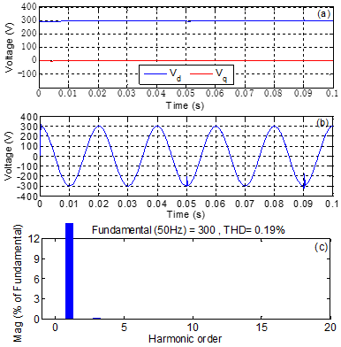
Figure 11(a) presents the dq components of the output voltage when the nonlinear load is connected at t = 0.05 s and disconnected at t = 0.09 s. It is clear that the control strategy with the proposed OSG operates appropriately since the Vdq components are equal to their references and the settling time is very small. Figure 11(b) illustrates the output voltage waveform. It can be noticed that although the applied heavy nonlinear load, the output voltage is quasi sinusoidal. Harmonic spectrum analysis of the generated VSI output voltage, illustrated in Figure 11(c), indicates zero amplitude error in steady-state and an insignificant THD (= 0.19%). Consequently, by means of the suggested control, the output voltage is undisturbed by the load current harmonics.
Figure 11. Simulation results in case of nonlinear load: (a) dq components of the output voltage, (b) output voltage waveform, and (c) harmonic spectrum of the output voltage
7.1 Description of the experimental setup
The proposed OSG for single-phase VSI control in SRF has been also evaluated by experiments. View of the experimental platform is shown in Figure 12. It mainly contains a DC source, a single-phase VSI, an LC filter, gate drives, and different sensors. The proposed control strategy, schematized in Figure 8, is implemented in MATLAB/Simulink environment and executed on a dSPACE DS1104 board. The experimental system parameters are given in Table 2.
Table 2. Experimental system parameters
|
VSI output AC voltage, Vmax |
155 |
|
VSI output voltage frequency, f |
50 Hz |
|
LC filter inductor, L |
5 mH |
|
LC filter capacitor, C |
5 µF |
|
Damping resistor, R |
8 Ω |
|
Sampling period, Ts |
95 µs |
|
Switching frequency, fsw |
10 KHz |
|
ADALINE learning rate, µ |
0.01 |
Figure 12. View of the experimental platform: (1) PC-Pentium + dSPACE board + ControlDesk, (2) dSPACE input/output connectors, (3) single-phase VSI, (4) DC source, (5) voltage and current sensors, and (6) nonlinear load
Several experimental tests are carried under different conditions. In what follows, the obtained results are illustrated and discussed. Initially, the proposed ADALINE-OSG is experimentally tested and compared to the conventional OSG [14] and two other advanced OSGs [15-18]. Thereafter, the suggested SRF voltage control that includes the proposed OSG is tested under highly nonlinear load. Robustness tests of the proposal under startup and step changes are also accomplished.
7.2 Performance evaluation of the proposed OSG
The purpose of this subsection is to experimentally compare the performances of the proposed OSG with other techniques. Indeed, the ADALINE-OSG is compared with the conventional TD based OSG (TD-OSG) [14] and two other advanced OSGs methods which are second order APF based OSG [16, 17] and HT based OSG (HT-OSG) [15, 18]. The transfer functions of second order APF based OSG and HT-OSG are given in Table 3. Performance evaluation of these OSGs is achieved with a nonlinear load.
Table 3. Transfer functions of HT-OSG and second order APF based OSG
|
Hilbert transform [15, 18] |
Second order APF [16, 17] |
|
$G(s)=\frac{{{\omega }_{b}}-s}{{{\omega }_{b}}+s}$ |
$G(s)=\frac{-\left( {{s}^{2}}-2{{\omega }_{n}}s+\omega _{n}^{2} \right)}{{{s}^{2}}+2{{\omega }_{n}}s+\omega _{n}^{2}}$ |
|
${{\omega }_{b}}=2\,\,\pi \,f\,;\,\,{{\omega }_{n}}=\left( \sqrt{2-1} \right){{\omega }_{b}}$ |
|
Figure 13. Performances comparison between the proposed OSG and others techniques: (a) d-axis voltage, and (b) d-axis current
Figure 13 illustrates the d-axis components of the output voltage and current for the four tested methods. Performances superiority of the proposed OSG is clearly shown by the obtained experimental results. Indeed, as it can be seen in Figure 13, superiority of the proposed ADALINE-OSG is clearly established in terms of efficiency, oscillations and stability compared to the other OSGs. Moreover, in case of the proposed OSG, the generated orthogonal signals are more filtered due to the ADALINE filtering capabilities.
Performances of the suggested SRF voltage control are also compared to those of the conventional SRF voltage control that uses the TD-OSG. Figures 14 and 15 illustrate the steady-state output voltage and its harmonic spectrum for both the proposed and conventional SRF voltage controls, respectively. The comparison tests are carried without any connected load.
Figure 14. Experimental results of the conventional SRF voltage control under no-load: (a) output voltage, and (b) harmonic spectrum of the output voltage
Figure 15. Experimental results of the proposed SRF voltage control under no-load: (a) output voltage, and (b) harmonic spectrum of the output voltage
As can be seen in Figures 14(a) and 15(a), the generated output voltage in case of the proposed control strategy is more stable and presented less oscillations compared to the output voltage generated in case of the conventional control strategy. In terms of THD, the proposed method shows an important harmonic reduction compared with the conventional method. Indeed, the obtained voltage THD in steady-state for the conventional method and the proposed method are 3.94% and 0.98%, respectively. Moreover, in terms of steady-state errors, the output voltage amplitude with the conventional method and the proposed method are 151.6 V and 154.7 V, respectively. So, the steady-state error in case of the conventional method and proposed method are 2.19% and 0.19% of the output voltage reference, respectively. From these results, it can be concluded that the suggested method yields a SRF voltage control scheme with better performances.
7.3 Performance evaluation of the proposed SRF voltage control under nonlinear load
As a worst-case operation, performances of the SRF voltage control including the proposed OSG has been tested in presence of a highly nonlinear load. Figure 16 shows the experimental results of the proposed SRF voltage control scheme at startup under nonlinear load. Initially, at t < 0.713 s, the output reference voltage |V*o| is fixed to 0 V. At t = 0.713 s, this reference steps from 0 V to 155 V. With short settling time, the output voltage and current are rapidly formed. Moreover, the generated waveforms are sinusoidal, stable and without overshoot. As can be seen in Figure 16(a), the output voltage amplitude |Vo| reaches its reference |V*o| within 2 cycles, which corresponds to 40ms. Therefore, convergence and stability of the controlled system is guaranteed at startup.
Figure 17 illustrates the steady-state output voltage and its harmonic spectrum when the supplied load is nonlinear. A regulated sinusoidal output voltage without any overshoot is obtained (see Figure 17(a)). In Figure 17(b), the harmonic spectrum of the output voltage is given. In this case, the output voltage THD is equal to 3.90%. Moreover, an insignificant steady-state error between the output voltage and its reference is obtained. Its value represents only 0.32% of the output voltage reference (155 V).
Figure 16. Experimental results of the proposed SRF voltage control at startup under nonlinear load: (a) output voltage, and (b) output current
Figure 17. Experimental results of the proposed SRF control at steady-state under nonlinear load: (a) output voltage, and (b) Harmonic spectrum of the output voltage
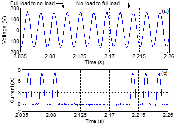
In another test, transient performances under nonlinear load step changes application are evaluated. In this case, the connected load varies from full-load to no-load at t = 2.1 s and disconnected at t = 2.2 s. Figure 18 illustrates the obtained VSI output voltage and current. As can be seen in Figure 18(a), the generated output voltage is sinusoidal and does not presents any overshoots during the load step changes. In addition, the output current dynamic is instantaneous under the load connection or disconnection.
Figure 19 illustrates the inverter system performances when the output voltage reference is stepped down to 50% under nonlinear load. At t = 0.95 s, the reference voltage amplitude steps from 155 V to 77.5 V. As can be seen in Figure 19(a), the output voltage reaches its steady-state value within a half cycle. Indeed, the output voltage amplitude |Vo| is superimposed with its reference |V*o| in about 9,5ms.
Figure 18. Experimental results of the proposed SRF voltage control under load step changes (from full-load to no-load and back): (a) output voltage, and (b) output current
Figure 19. Experimental results of the proposed SRF voltage control when |V*o| is stepped down to 50% under nonlinear: (a) output voltage, and (b) output current
This paper presented an enhanced SRF voltage control of a single-phase VSI operating in a stand-alone mode. A new ADALINE-OSG has been developed to extend the single-phase VSI into a three-phase equivalent system. The use of the ADALINE technique has been motivated by its filtering capabilities, simple structure and convergence speed. The proposed SRF voltage control has been significantly simplified since the proposed OSG is able to generate and to filter the orthogonal component, to provide the dq components, and to identify the harmonic residue. The proposed OSG has been experimentally tested and compared with the conventional OSG and two other advanced OSGs. Its superiority in terms of efficiency oscillations and stability has been clearly established. Moreover, performances of the suggested SRF voltage control scheme have been evaluated by means of simulations and experiments. Obtained results have shown insignificant steady-state errors and low harmonic distortions in the VSI output voltage. Dynamic performances under load disturbance are also experimentally checked. It is found that the settling time, voltage sag, and overshoot in the resulted output voltage are very small. Hence, considering the filtering capability of the proposed OSG and its ability to provide the αβ and dq components, it has been concluded that the suggested SRF voltage control yields to a simplified control with better performances. So, the proposed control scheme can be easily integrated into more complex system, such as standalone hybrid renewable energy generation systems.
This work was supported by the Franco-Algerian cooperation program PHC-TASSILI (Project No. 17MDU995).
|
C |
filter capacitor |
|
Cidq |
compensation terms |
|
e(k) |
ADALINE error |
|
f |
VSI output voltage frequency |
|
h(t) |
distortion harmonics |
|
i, iL |
inductor and inverter output current |
|
icαβ, iLαβ iαβ |
capacitor, inverter output and inductor currents in αβ frame |
|
Icdq, ILdq, Idq |
capacitor, inverter output and inductor currents in dq frame |
|
kh |
proportional gain of harmonics cancelation |
|
ki, kv |
proportional gains of the inner and outer control loop |
|
L |
filter inductor |
|
R |
damping resistor |
|
Ts |
sampling period |
|
Udq, uαβ |
duty cycles in dq and αβ frames |
|
u’dq |
duty cycle references in dq frame |
|
uref |
duty cycle reference |
|
u’ref |
duty cycle reference ensuring harmonics cancelation |
|
v |
inverter output voltage |
|
Vdc |
DC bus voltage |
|
Vdq, vαβ |
inverter output voltage in dq and αβ frames |
|
vf |
fundamental component of the output voltage |
|
W (k) |
ADALINE weights vector |
|
Xd, Xq |
dq components |
|
Xm |
amplitude of fundamental signal |
|
Xm-n |
output voltage amplitude of the nth order harmonic |
|
X (k) |
ADALINE input vector |
|
yd(k), yest (k) |
desired signal and estimated output of the ADALINE |
|
Greek symbols |
|
|
µ |
ADALINE learning rate |
|
ωf |
pulsation of the fundamental component |
|
θ |
Park angle |
|
φ |
initial phase of the fundamental component |
|
φn |
output voltage phase of the nth order harmonic |
|
τi, τv |
time constant inner and outer control loop time constant |
[1] Stojić, D., Georgijević, N., Rivera, M., Milić, S. (2018). Novel orthogonal signal generator for single phase PLL applications. IET Power Electronics, 11(3): 427-433. http://doi.org/10.1049/iet-pel.2017.0458
[2] Zheng, L.J., Jiang, F.Y., Song, J.C., Gao, Y.G., Tian, M.Q. (2018). A discrete-time repetitive sliding mode control for voltage source inverters. IEEE Journal of Emerging and Selected Topics in Power Electronics, 6(3): 1553-1566. https://doi.org/10.1109/jestpe.2017.2781701
[3] Parvez, M., Elias, M.F.M., Rahim, N.A., Blaabjerg, F., Abbott, D., Al-Sarawi, S.F. (2020). Comparative study of discrete PI and PR controls for single-phase UPS inverter. IEEE Access, 8: 45584-45595. https://doi.org/10.1109/ACCESS.2020.2964603
[4] Rymarski, Z., Bernacki, K. (2020). Different features of control systems for single-phase voltage source inverters. Energies, 13(16): 4100. https://doi.org/10.3390/en13164100
[5] Rymarski, Z. (2012). Control systems of single-phase voltage source inverters for a UPS. IFAC Proceedings Volumes, 45(7): 316-321. https://doi.org/10.3182/20120523-3-cz-3015.00060
[6] Khajehoddin, S.A., Karimi-Ghartemani, M., Jain, P.K., Bakhshai, A. (2012). A resonant controller with high structural robustness for fixed-point digital implementations. IEEE Transactions on Power Electronics, 27(7): 3352-3362. https://doi.org/10.1109/tpel.2011.2181422
[7] Komurcugil, H. (2012). Rotating-sliding-line-based sliding-mode control for single-phase UPS inverters. IEEE Transactions on Industrial Electronics, 59(10): 3719-3726. http://doi.org/10.1109/TIE.2011.2159354
[8] Dasgupta, S., Sahoo, S.K., Panda, S.K. (2011). Single-phase inverter control techniques for interfacing renewable energy sources with microgrid-Part I: Parallel-connected inverter topology with active and reactive power flow control along with grid current shaping. IEEE Transactions on Power Electronics, 26(3): 717-731. https://doi.org/10.1109/tpel.2010.2096479
[9] Buso, S., Caldognetto, T., Brandao, D.I. (2016). Dead-beat current controller for voltage-source converters with improved large-signal response. IEEE Transactions on Industry Applications, 52(2): 1588-1596. https://doi.org/10.1109/TIA.2015.2488644
[10] Deng, H., Oruganti, R., Srinivasan, D. (2003). A neural network-based adaptive controller of single-phase inverters for critical applications. The Fifth International Conference on Power Electronics and Drive Systems, Singapore, pp. 915-920. https://doi.org/10.1109/peds.2003.1283090
[11] Sun, X., Chow, M.H.L., Leung, F.H.F., Xu, D., Wang, Y., Lee, Y.S. (2002). Analogue implementation of a neural network controller for UPS inverter applications. IEEE Transactions on Power Electronics, 17(3): 305-313. https://doi.org/10.1109/TPEL.2002.1004238
[12] Deng, H., Oruganti, R., Srinivasan, D. (2008). Neural controller for UPS inverters based on B-spline network. IEEE Transactions on Industrial Electronics, 55(2): 899-909. https://doi.org/10.1109/tie.2007.909064
[13] Bay, O.F., Atacak, I. (2007). Realization of a single phase DSP based neuro-fuzzy controlled uninterruptible power supply. IEEE International Symposium on Industrial Electronics. Vigo, Spain, pp. 707-712. https://doi.org/10.1109/isie.2007.4374683
[14] Roshan, A., Burgos, R., Baisden, A.C., Wang, F., Boroyevich, D. (2007). A DQ frame controller for a full-bridge single phase inverter used in small distributed power generation systems. IEEE Applied Power Electronics Conference and Exposition, Anaheim, USA, pp. 641-647. https://doi.org/10.1109/APEX.2007.357582
[15] Ebrahimi, M., Khajehoddin, S.A., Karimi-Ghartemani, M. (2016). Fast and robust single-phase DQ current controller for smart inverter applications. IEEE Transactions on Power Electronics, 31(5): 3968-3976. https://doi.org/doi: 10.1109/TPEL.2015.2474696
[16] Monfared, M., Golestan, S., Guerrero, J.M. (2014). Analysis, design, and experimental verification of a synchronous reference frame voltage control for single-phase inverters. IEEE Transactions on Industrial Electronics, 61(1): 258-269. http://doi.org/10.1109/TIE.2013.2238878
[17] Choi, J., Kim, Y., Kim, H. (2006). Digital PLL control for single-phase photovoltaic system. IEE Proceedings-Electric Power Application, 153(1): 40-46. http://doi.org/10.1049/ip-epa:20045225
[18] Liao, Y., Liu, Z., Zhang, H., Wen, B. (2018). Low-frequency stability analysis of single-phase system with dq-frame impedance approach-Part I: Impedance modeling and verification. IEEE Transactions on Industry Applications, 54(5): 4999-5011. http://doi.org/10.1109/TIA.2018.2832027
[19] Du, H., Sun Q.Y., Cheng, Q.F., Ma, D.Z., Wang, X. (2019). An adaptive frequency phase-locked loop based on a third order generalized integrator. Energies, 12(2): 309. https://doi.org/10.3390/en12020309
[20] Huang, X., Dong, L., Xiao, F., Liao, X. (2016). A new orthogonal signal generator with DC offset rejection for single-phase phase locked loops. Journal of Power Electronics, 16(1): 310-318. https://doi.org/10.6113/JPE.2016.16.1.310
[21] Lamo, P., Pigazo, A., Azcondo, F.J. (2020). Evaluation of quadrature signal generation methods with reduced computational resources for grid synchronization of single-phase power converters through phase-locked loops. Electronics, 9(12): 2026. https://doi.org/10.3390/electronics9122026
[22] Zhang, C., Ge, X., Ma, J. (2017). A fast instantaneous power calculation algorithm for single-phase rectifiers based on arbitrary phase-delay method. IEEE Transportation Electrification Conference and Expo, Asia-Pacific (ITEC Asia-Pacific). Harbin, pp. 1-6 https://doi.org/10.1109/itec-ap.2017.8080927
[23] Bei, T.Z., Wang, P. (2016). Robust frequency-locked loop algorithm for grid synchronisation of single-phase applications under distorted grid conditions. IET Generation, Transmission & Distribution, 10(11): 2593-2600. https://doi.org/10.1049/iet-gtd.2015.0914
[24] Widrow, B., Lehr, M.A. (1990). 30 years of adaptive neural networks: perceptron, Madaline, and backpropagation. Proc IEEE, 78(9): 1415-1442. https://doi.org/10.1109/5.58323
[25] Goodwin, G.C., Sin, K.S. (1994). Adaptive Filtering Prediction, and Control. Englewood Cliffs, NJ: Prentice Hall.