Conduction Band Offset Effect on the Cu2ZnSnS4 Solar Cells Performance

Ahmed Redha Latrous* | Ramdane Mahamdi | Naima Touafek | Marcel Pasquinelli
© 2021 IIETA. This article is published by IIETA and is licensed under the CC BY 4.0 license (http://creativecommons.org/licenses/by/4.0/).
OPEN ACCESS
Among the causes of the degradation of the performance of kesterite-based solar cells is the wrong choice of the n-type buffer layer which has direct repercussions on the unfavorable band alignment, the conduction band offset (CBO) at the interface of the absorber/buffer junction which is one of the major causes of lower VOC. In this work, the effect of CBO at the interface of the junction (CZTS/Cd(1-x)ZnxS) as a function of the x composition of Zn with respect to (Zn+Cd) is studied using the SCAPS-1D simulator package. The obtained results show that the performance of the solar cells reaches a maximum values (Jsc = 13.9 mA/cm2, Voc = 0.757 V, FF = 65.6%, ɳ = 6.9%) for an optimal value of CBO = -0.2 eV and Zn proportion of the buffer x = 0.4 (Cd0.6Zn0.4S). The CZTS solar cells parameters are affected by the thickness and the concentration of acceptor carriers. The best performances are obtained for CZTS absorber layer, thichness (d = 2.5 µm) and (ND = 1016 cm-3). The obtained results of optimizing the electron work function of the back metal contact exhibited an optimum value at 5.7 eV with power conversion efficiency of 13.1%, Voc of 0.961 mV, FF of 67.3% and Jsc of 20.2 mA/cm2.
absorber layer, buffer layer, CBO, Cd(1-x)ZnxS, CZTS, interface, SCAPS-1D, solar cell
A recent explosion of Kesterite Cu2ZnSn(S,Se)4 (CZTSSe) solar cells has led scientists to adopt extensive research towards this surprising absorbent thin-film technology considered to be the ideal materials because of their environmental affinities, the abundance of its constituent elements on the ground, their direct band gaps (1-1.5 eV) without forgetting their high absorption coefficients compared to their counterparts, chalcopyrite, chalcogenide and perovskite [1-5].The progress of experimental research aimed at improving the performance of this type of material has revealed a conversion efficiency of 12.6% for the sulfur-selenium alloy CZTSSe [6], 11.6% for the compound based on Selenium CZTSe [7], while a yield greater than 9% characterized the compound based on pure sulfur CZTS [8]. Despite all the efforts made in this discipline, the best performance for Kesterite remains below their neighbors, chalcopyrites, in particular solar cells based on Cu2InGaS4 [9, 10] and CdTe [11]. Worth mentioning that the absorbent layer CZTS contains non-toxic elements, absence of selenium Se and therefore more ecological than the CZTSSe semiconductor. Also, CZTS semiconductor structure is very analogous to chalcopyrite semiconductors, which allows applying their different technologies.
Despite all the qualities mentioned, CZTS cells constantly endure from weak electronic properties, mainly due to the high recombination of carriers in the interface between the absorber (CZTS) and the buffer layers where the atomic arrangement is extremely disordered and then conversion efficiency of the CZTS absorber solar cells is mainly limited by the significant deficit of open circuit voltage (Voc). Several factors could reduce the Voc among them the unwanted energy bands alignment at the absorber/buffer heterojunction, which can cause strong recombination at these interfaces [12]. Different values of conduction band offset (CBO) have been described [13]. From first-principles calculations, CBO is reported to be “cliff”-like and most recent investigations including measurements admit that the “cliff”-like CBO acts significantly to the interface recombination and thereby VOC deficit. The “cliff” creation would act as a barrier to stop the flow of injected electrons (majority carrier) from the buffer to the absorber under forward bias [14, 15]. To remedy this in terms of the VOC deficit and avoid the degradation of the performance of our kesterite cell, the choice of the buffer layer is essential in order to reduce the losses by recombination at the interface of the absorber/buffer junction.
Much research work on the effect of band offsets at the absorber/buffer interfaces has been undertaken primarily for the ZnS and CdS buffer layers [16]. The conduction band minimum (CBM) of the ZnS as a buffer layer in the CZTS solar cells is located above the CBM of the CZTS absorber layer, then it forms barrier to photo generated electrons and leads to high carrier losses, whereas in the case of CdS its CBM is located below the CBM of the CZTS absorber layer causing a large negative CBO which increases the interface recombination. In this perspective, and throughout our study, a good compromise concerning the buffer layer Cd(1-x)ZnxS with convenient band gaps which will be chosen so that its CBM can be chosen by controlling the Zn/(Zn + Cd) ratio of cadmium to zinc. This represents the main goal of our work to optimize the buffer layer Cd(1–x)ZnxS according to x by calculating with the SCAPS-1D Software, the energy bands alignment CBO at the interface of the CZTS/Cd(1–x)ZnxS junction and thus contributes to the improvement of the output performance of the proposed structure SLG/Mo/CZTS/Cd(1–x)ZnxS/ZnO:Al, the open circuit voltage VOC, the short-circuit current density JSC, as well as the Fill factor FF and the efficiency $\eta$ by simulating the effects of various electrical and optical parameters, the absorber layer thickness, the acceptor carrier concentration of the absorber layer as well as the predominant impact of electron work function of the back metal contact. Our proposed structure and numerical calculations will be exposed in the following sections.
Our structure SLG/Mo/CZTS/Cd(1–x)ZnxS/ZnO:Al, as illustrated in Figure 1 has been adopted as the basic model throughout our study, knowing that many authors have experimentally analyzed its behavior [17]. In this structure SLG (Soda Lime Glass) acts as substrate, followed by Mo which acts as back contact over which there is a thin layer p-type doped CZTS kesterite which acts as absorber active layer. A thin n-doped Cd(1–x)ZnxS layer with direct band gap tunable between 2.64 eV (x = 0) and 3.42 eV (x = 1) and the electronic affinity which varies between 4.8 eV (x = 0) and 3.9 (x = 1) is deposited on the CZTS layer, followed by a ZnO type n window layer, which acts as front contact on which aluminum contacts are grown.
Figure 1. Proposed CZTS Kesterite structure
SCAPS-1D solar simulation software for thin layer solar cells developed at Gent University is exploited to inject the device parameters as well as material parameters of each layer based on solving the Poisson equation and electron-hole continuity equations [18].
The physical parameters are selected from the literature values and were listed in Table 1 [19-21]. The absorption coefficients for all materials used in this study are taken from Scaps. We opted for an operating temperature set at 300°K. Solar radiation is incident at the front contact with Air mass 1.5 global spectrum (AM1.5G) and a solar light power of (103 W/m2) and taking into account series resistance 3.25 Ω and shunt resistance 400 Ω.
In Table 1, we fixed the thicknesses values of the buffer layers Cd(1-x)ZnxS as well as the window layer and we varied the thickness of the absorbent layer CZTS. We have also fixed respectively the values of the bandgaps and the electronic affinities of the absorbent and window layers. We have also fixed the values of the density of donor atoms for the buffer and window layers; by varying the density of acceptor atoms for the absorbent layer CZTS. We supposed that the electron work function of the back metal contact is variable [21]. The effects of radiative recombination and Auger electron/hole captures have been considered throughout all the cases. It should also be noted that the defects influence at the various interfaces (CZTS/Cd(1–x)ZnxS) and (Cd(1–x)ZnxS/ZnO) is not taken into account.
Table 1. Physical values for the different layers of the proposed structure
|
Parameters |
CZTS |
Cd(1-x)ZnxS |
ZnO:Al |
|
Thickness [µm] |
Var |
0.05 |
0.2 |
|
Bandgap Eg [eV] |
1.5 |
Var |
3.35 |
|
Electron affinity χ [eV] |
4.25 |
Var |
4.4 |
|
Relative dielectric permittivity er [eV] |
10 |
10 |
9 |
|
NC [cm-3] |
2.2×10¹⁸ |
2.2×10¹⁸ |
2.2×10¹⁸ |
|
NV [cm-3] |
1.8×10¹⁹ |
1.8×10¹⁹ |
1.8×10¹⁹ |
|
Electron themal velocity [cm/s] |
1×10⁷ |
1×10⁷ |
1×10⁷ |
|
Hole themal velocity [cm/s] |
1×10⁷ |
1×10⁷ |
1×10⁷ |
|
Electron mobility µn [cm2/V.s] |
1×10² |
1×10² |
1×10² |
|
Hole mobility µp [cm2/V.s] |
2.5×101 |
2.5×101 |
2.5×101 |
|
Donor density ND [cm-3] |
1×101 |
1×10¹⁷ |
1×10¹⁸ |
|
Acceptor density NA [cm-3] |
Var |
0 |
0 |
|
Absorption coefficient α [cm-1] |
Scaps |
Scaps |
Scaps |
|
Radiative recombination coefficient Br [cm3/s] |
5×10⁻⁹ |
- |
- |
|
Auger electron capture coefficient [cm6/s] |
1×10-29 |
- |
- |
|
Auger hole capture coefficient [cm6/s] |
1×10-29 |
- |
- |
|
Defect type (A/D/N) |
A:8.5×10¹⁵ |
D:1×10¹⁷ |
D:1×10¹⁸ |
|
Defect density [cm-3] |
7×10¹⁵ |
5×10¹⁶ |
1×10¹⁶ |
NC – Conduction band effective density of states, NV – Valence band effective density of states
3.1 Energy bands calculation
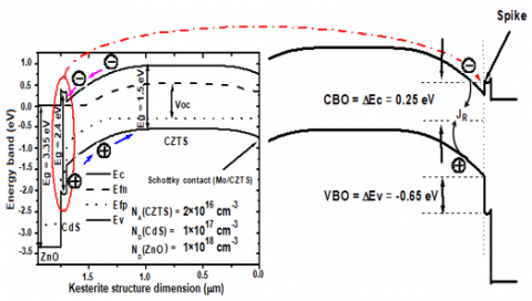
Before optimization, the first step of this work consists in simulating and validating by the SCAPS 1D software the basic structure proposed SLG/Mo/CZTS/CdS/ZnO:Al with the experimental results [19]. The energy band alignment diagram for the non-equilibrium condition of the different layers is shown in Figure 2 as a function of the parameters summarized in Table 1, showing the offsets of the conduction and valence band as well as the different band gap and electron affinities at the CZTS/CdS junction interface. The band gap energy of the buffer layer is 2.4 eV and its electron affinity is 4.0 eV. The CBO and the VBO of this junction both are negative, which causes an increase in the carriers recombination and consequently a decrease in Voc, due to the activation energy relatively lower than the absorber band gap [22, 23]. This band offset causes significant minority charge recombination, thus the Voc value is reduced Figure 3. The formation of the heterojunction brings about the alignment of the Fermi level of the bands of all the layers in equilibrium with the vacuum level. Under illumination, excess free carriers are generated and the Fermi level subdivides into quasi-Fermi levels due to the open circuit voltage Voc. According to the results of the energy band diagram calculations, there is a spike-like CBO at the interface of the CZTS/CdS heterojunction Figure 3. The electron affinity of CdS (~4 eV) is lower than that of CZTS (~4.25 eV) which will generate a positive spike-like CBO with DEc = 0.25eV which prevent the movement of electrons from the kesterite layer to the buffer layer and a negative valence band offset VBO with DEv = -0.65 eV.
Figure 2. Energy band diagram representation of the basic kesterite structure
Figure 3. Simulated energy band diagram of the basic kesterite structure before optimization
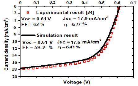
Figure 4. Comparison between experimentation and J-V characteristics of the structure before optimization
3.2 Characteristics current density-voltage (J-V) simulation and validation
To validate the model of the basic structure before optimization and under lighting, the curve representing the current density as a function of the voltage (J-V) was simulated and compared to the experimental curve [24] in accordance with the parameters exhibited in Table 1. There is a good agreement between the experimentation and simulation curves which validates our set of parameters as a baseline for the simulation in this work Figure 4.
3.3 Influence of [Zn]/([Zn]+[Cd]) rate of Cd(1-x)ZnxS buffer layer
In this section, we review the study of the impact of [Zn] / ([Zn] + [Cd]) rate of the Cd(1-x)ZnxS thin layer on energy bands alignment, therefore on the conduction bands offsets (CBO) and the valence bands offsets (VBO) leading to the spike or cliff creation at the interface of the buffer/absorber junction. These bands offsets prevent the two types of carriers, electrons and holes from moving and crossing these obstacles. We are therefore witnessing a strong recombination at the CZTS/Cd(1-x)ZnxS junction interface and inside the device, producing performance degradation of the structure. In this perspective, pushed computations by the SCAPS-1D simulator were undertaken in such a way as to introduce a promising buffer layer Cd(1-x)ZnxS into the basic structure, by varying the rate x between the value 0 (CdS) and the value 1 (ZnS), its band gap therefore varies respectively between 2.64 eV and 3.42 eV as well as the electron affinity between 4.8 eV and 3.9 eV. Bandgap and electron affinity of Cd(1-x)ZnxS for different Zn composition can be calculated by extrapolation of experimental curves [25, 26] given by the Eqns. (1) and (2), in the other hand, the CBO and VBO are deduced from the Eqns. (3) and (4).
$\operatorname{Eg}\left(\mathrm{Cd}_{(1-\mathrm{x})} \mathrm{Zn}_{\mathrm{x}} \mathrm{S}\right)=2.642+1.067 \mathrm{x}-0.285 \mathrm{x}^{2}(\mathrm{eV})$ (1)
$\chi\left(\mathrm{Cd}_{(1-\mathrm{x})} \mathrm{Zn}_{\mathrm{x}} \mathrm{S}\right)=4.8-0.9 \mathrm{x}(\mathrm{eV})$ (2)
$\Delta \mathrm{E}_{\mathrm{C}}=\chi(\mathrm{CZTS})-\chi\left(\mathrm{Cd}_{(1-\mathrm{x})} \mathrm{Zn}_{\mathrm{x}} \mathrm{S}\right)(\mathrm{eV})$ (3)
$\left.\Delta \mathrm{E}_{\mathrm{V}}=\left[\mathrm{E}_{\mathrm{g}}(\mathrm{CZTS})+\chi(\mathrm{CZTS}\right)\right]-\left[\mathrm{E}_{\mathrm{g}}\left(\mathrm{Cd}_{(1-\mathrm{x})} \mathrm{Zn}_{\mathrm{x}} \mathrm{S}\right)++\chi\left(\mathrm{Cd}_{(1-\mathrm{x})} \mathrm{Zn}_{\mathrm{x}} \mathrm{S}\right)\right](\mathrm{eV})$ (4)
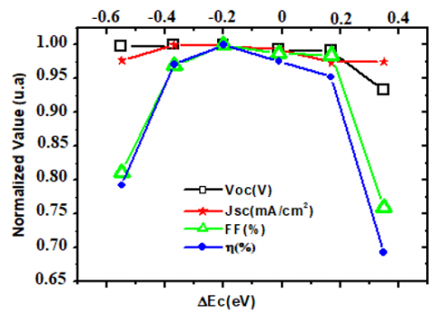
All the simulated computations representing energy bands alignment of the conduction and valence bands as a function of the dimensions of the proposed cell are represented in Figure 5. It has been observed that the CBO at The CZTS/Cd(1-x)ZnxS plays a large role in controlling the carriers transmission through the metallic contact. The amount of this offset is determined by the difference in the buffer/absorber layer’s electron affinity. The increase in positive and negative band offsets would respectively form spike-like and cliff-like structures. With increasing electron affinity of the buffer layer, the junction interface CZTS/Cd(1-x)ZnxS would change from a spike-like shape to another cliff-like shape. In order to determine the conduction band offset CBO, the impact of DEc on VOC, JSC, FF and $\eta$ was simulated. The recombination process at the CZTS/Cd(1-x)ZnxS layer interface has already been treated by several authors [27]. In fact energy band diagram of the SLG/Mo/CZTS/Cd(1-x)ZnxS/ZnO:Al solar system in Figure 5 illustrates the easy electrons transfer from the CZTS absorber layer to the front contact through the Cd(1-x)ZnxS/ZnO:Al interface. The highest conversion efficiency and FF obtained are 6.9% and 65.6% respectively at an optimum value of CBO = -0.2eVfor the value of x equal to 0.4. However the values of VOC and JSC are respectively 0.757 V and 13.9 mA/cm2 for the same optimal value of CBO. Nonetheless, out of this range, we can observe a decrease in the FF and the efficiency parameters Figure 6. The recombination phenomenon, which is the main factor in the reduction of the quantum efficiency, is consistent with the reduction in the fill factor and short- circuit current. It can also be concluded that the VBO negative values are not an obstacle in the shift of carriers from the surface at the absorber/buffer interface to the absorber layer, and do not significantly change the solar cell’s performance. As a result the CBO will be a determining factor in improving the produced optical flow and increasing efficiency.
Figure 5. Energy band diagram evolution of the proposed structure
Figure 6. Variation of VOC, JSC, FF and $\eta$ with CBO at the CZTS/Cd(1-x)ZnxS junction interface of the proposed structure
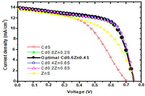
Figure 7. J-V characteristics of the proposed structure before optimization according to Cd(1−x)ZnxS buffer layers
Simulation results of the proposed structure using alternative buffer layers Cd(1-x)ZnxS instead of the standard buffer layer CdS show that these thin-film semiconductor materials are suitable to participate in improving the performance of the device by adopting as an optimal layer, the buffer layer Cd0.6Zn0.4S. The characteristic J-V of all the kesterite structure parameterized by the variation of the buffer layer Cd(1-x)ZnxS is illustrated in Figure 7. For all these reasons, this buffer layer will represent the most appropriate layer used in order to optimize the parameters of the structure.
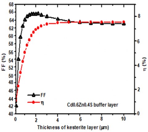
3.4 CZTS absorbent layer thickness influence
After having optimized the buffer layer Cd0.6Zn0.4S, we will place particular emphasis on other factors influencing the performance of the proposed structure, in particular the thickness of the absorbent layer [28, 29]. To analyze its impact, calculations were made for different thicknesses of the CZTS absorber layer ranging from 10 nm to 10 µm, this layer, assuming all other parameters constant as described in the Table 1. As shown in Figure 8, the curves obtained after simulation show that by increasing the thickness of the absorber from 200 nm to 10000 nm, Voc, Jsc, FF and $\eta$ increase accordingly. We can also notice that Voc has increased by around 20%, while JSC has decreased by 18%. FF and the conversion efficiency were consequently increased by 10% and 11% respectively compared to the basic structure before optimization. A good improvement was noted for an optimum absorber thickness of 2.5 µm.
Figure 8. Variation of VOC, JSC, FF and $\eta$ as a function of CZTS absorber layer thickness
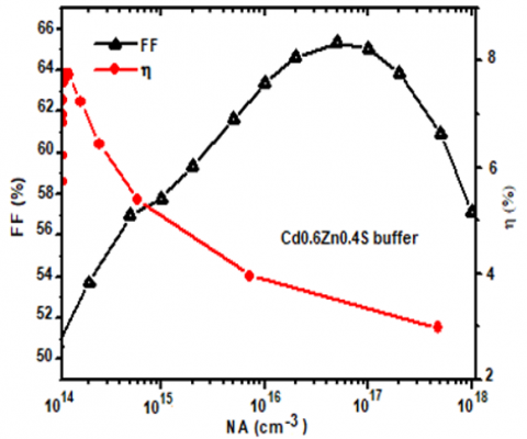
3.5 Acceptor carrier concentration influence of the CZTS absorber layer
Likewise, the acceptor carrier concentration NA of CZTS absorber thin layer plays a major role in improving the performance of the structure. From this perspective one of the aims of our paper is to study its effect on the overall efficiency of our solar cell [28, 29]. After setting the optimum value for the CZTS absorbent layer thickness at 2.5 mm, we note the normalized output parameters (VOC = 0.825 V, JSC = 23.5 mA/cm2, FF = 65.3%, $\eta$ = 7.7%) in Figure 9. As carrier concentration increases from 1×1014 cm-3 to 1×1018 cm-3, the semiconductor becomes degenerate; this is one of the major concerns for limiting the higher value of NA. This will generate a reduction in the space charge region of the absorber side which in turn leads to a sharp diminution of the photo generated carriers in this region [21], and therefore a decrease in the current density Jsc and the energy conversion efficiency. A good improvement was also noted for an optimum acceptor carrier concentration NA of 1×1016 cm-3.
Figure 9. Variation of VOC, JSC, FF and $\eta$ as a function of CZTS absorber layer acceptor carrier concentration
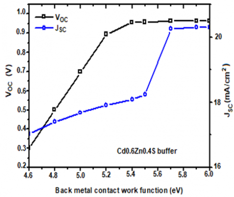
3.6 Back metal contact work function influence of the CZTS absorber layer
The influence of the back metal contact work function (BMWF) is taken into account in this work. After setting the optimum value for the CZTS absorbent layer thickness at 2.5mm and the optimum value for acceptor carrier concentration NA at 1×1016 cm-3, and to find the influence of the electron work function $\phi$ of metal at the back contact, its value in the range from 4.6 eV to 6 eV was varied in the simulation. By an increase in the BMWF an incredible improvement in solar cell parameters was found, as revealed from Figure 10 (VOC = 0.961 V, JSC = 20.2 mA/cm2, FF = 67.3%, $\eta$ = 13.1%). A remarkably sharp rise is observed for BMWF in the range of 5.2 – 6 eV, where JSC can reach up to around 20 mA/cm2 similar to the authors [30] due to improve of the interface CZTS/Mo by a good ohmic contact. The conversion efficiency remains almost constant for BMWF between 5.7 and 6 eV. According to the graph, the optimal value is located at 5.7 eV.
Figure 10. Variation of VOC, JSC, FF and $\eta$ as a function of CZTS absorber layer back metal contact work function
In this paper, the impact of conduction band offset (CBO) at the absorber/buffer (CZTS/Cd(1-x)ZnxS) junction interface was investigated using SCAPS-1D software.
We calculated a large negative value of -0.55eV for the "cliff" like CBO at the CZTS/CdS junction interface for a proportion of the buffer x = 0, which represents one of the main recombination mechanisms, whereas a calculated value of 0.35 eV for the "spike" like CBO at the interface of the CZTS/ZnS junction for a proportion of the buffer x = 1 shows the formation of a barrier to the photo generated electrons and leads to high carriers losses. The results obtained are in good agreement with the works already published by the authors.
The variation of the proportion x between 0 and 1 allowed us to simulate a new buffer layer Cd0.6Zn0.4S, reduce the recombination at the interface of the junction as well as the deficit of VOC and therefore improve the efficiency of our cell. For this buffer layer the results show an improvement in VOC of 7% compared to ZnS and a clear improvement in efficiency of 30% compared to ZnS and 20% compared to CdS.
The obtained maximum values (VOC = 961 mV, JSC = 20.2 mA/cm2, FF = 67.3% and $\eta$ = 13.1%) are both reached at an optimal cliff value around -0.2 eV for a composition x = 0.4 (Cd0.6Zn0.4S) and optimal absorber CZTS layer. The optimized values of these parameters were 2.5 mm for CZTS layer thickness, 1×1016 cm-3 for the acceptor doping concentration NA, and 5.7 eV for the Molybdenum back metal contact work function (BMWF).
Authors acknowledge Dr. Marc Burgelman and colleagues from University of Gent for using SCAPS-1D program in all simulations reported in this paper.
[1] Mekky, A.H. (2020). Electrical and optical simulation of hybrid perovskite-based solar cell at various electron transport materials and light intensity. Annales de Chimie - Science des Matériaux, 44(3): 179-184. https://doi.org/10.18280/acsm.440304
[2] Touafek, N., Mahamd,i R., Dridi, C. (2019). Impact of the secondary phase ZnS on CZTS performance solar cells. International Journal of Control, Energy and Electrical Engineering, 9: 6-9.
[3] Vauche, L., Risch, L., Sanchez, Y., Dimitrievska, M., Pasquinelli, M., Goislard de Monsabert, T., Grand, P.P., Jaime-Ferrer, S., Saucedo, E. (2015). 8.2% pure selenide kesterite thin-film solar cells from large-area electrodeposited precursors. Progress in Photovoltaics: Research and Applications, 24(1): 38-51. https://doi.org/10.1002/pip.2643
[4] Vauche, L., Dubois, J., Laparre, A., Pasquinelli, M., Bodnar, S., Grand, P.P., Jaime, S. (2014). Rapid thermal processing annealing challenges for large scale Cu2ZnSnS4 thin films. Physica Status Solid: Applications and Materials Science, 212(1): 103-108. https://doi.org/10.1002/pssa.201431387
[5] Ruiz, C.M., Pérez-Rodriguez, A., Arbiol. J., Morante, J.R., Bermúdez, V. (2014). Impact of the structure of Mo(S,Se)2 interfacial region in electrodeposited CuIn(S,Se)2 solar cells. Physica Status Solid: Applications and Materials Science, 212(1): 61-66. https://doi.org/10.1002/pssa.201431435
[6] Wang, W., Winkler, M.T., Gunawan, O., Gokmen, T., Todorov, T.K., Zhu, Y., Mitzi, D.B. (2013). Device characteristics of CZTSSe thin‐film solar cells with 12.6% efficiency. Advanced Energy Materials, 4(7):1301465. https://doi.org/10.1002/aenm.201301465
[7] Lee, Y.S., Gershon, T., Gunawan, O., Todorov, T.K., Gokmen, T., Virgus, Y., Guha, S. (2015). Cu2ZnSnSe4 thin‐film solar cells by thermal co‐evaporation with 11.6% efficiency and improved minority carrier diffusion length. Advanced Energy Materials, 5(7): 1401372. https://doi.org/10.1002/aenm.201401372
[8] Hao, X., Sun, K., Yan, C., Liu, F., Huang, J., Pu, A., Green, M. (2016). Large VOC improvement and 9.2% efficient pure sulfide Cu2ZnSnS4 solar cells by heterojunction interface engineering. IEEE 43rd Photovoltaic Specialists Conference (PVSC), Portland, OR, USA, pp. 5-10. https://doi.org/10.1109/PVSC.2016.7750017
[9] Touafek, N., Mahamdi, R. (2014). Excess defects at the CdS/CIGS interface solar cells. Chalcogenide Letters, 11(11): 589-596.
[10] Touafek, N., Mahamdi, R. (2014). Back surface recombination effect on the ultra-thin CIGS solar cells by SCAPS. International Journal of Renewable Energy Research, 4(4): 958-964.
[11] Akbarnejad, E., Ghorannevis, Z., Mohammadi, E., Fekriaval, L. (2019). Correlation between different CdTe nanostructures and the performances of solar cells based on CdTe/CdS heterojunction. Journal of Electroanalytical Chemistry, 849: 113358. https://doi.org/10.1016/j.jelechem.2019.113358
[12] Kaur, K., Kumar, N., Kumar, M. (2017). Strategic review of interface carrier recombination in earth abundant Cu–Zn–Sn–S–Se solar cells: Current challenges and future prospects. Journal of Materials Chemistry A, 5: 3069-3090. https://doi.org/10.1039/C6TA10543B
[13] Kumar, A., Thakur, A.D. (2018). Role of contact work function, back surface field and conduction band offset in CZTS solar cell. Japanese Journal of Applied Physics, 57(8S3): 08RC05. https://doi.org/10.7567/JJAP.57.08RC05
[14] Liu, X., Feng, Y., Cui, H., Liu, F., Hao, X., Conibeer, G., Mitzi, D.B., Green, M. (2016). The current status and future prospects of kesterite solar cells: A brief review. Progress in Photovoltaic, 24(6): 879-898. https://doi.org/10.1002/pip.2741
[15] Pal, K., Singh, P., Bhaduri, A., Thapa, K.B. (2019). Current challenges and future prospects for a highly efficient (> 20%) kesterite CZTS. Solar Energy Materials and Solar Cells, 196: 138-156. https://doi.org/10.1016/j.solmat.2019.03.001
[16] Wang, D., Zhao, W., Zhang, Y., Liu, S. (2018). Path towards high-efficient kesterite solar cells. Journal of Energy Chemistry, 27(4): 1040-1053. https://doi.org/10.1016/j.jechem.2017.10.027
[17] Khattak, Y.H., Baig, F., Ullah, S., Mari, B., Beg, S., Ullah, H. (2018). Enhancement of the conversion efficiency of thin film kesterite solar cell. Journal of Renewable and Sustainable Energy, 10(3): 033501. https://doi.org/10.1063/1.5023478
[18] Niemegeers, A., Burgelman, M., Decock K, et al. (2013). Scaps Manual, e-Book.
[19] Haddout, A., Raidou, A., Fahoume, M., Elharfaoui, N., Lharch, M. (2018). Influence of CZTS layer parameters on cell performance of kesterite thin-film solar cells. Proceedings of the 1st International Conference on Electronic Engineering and Renewable Energy, Saidia, Morocco, pp. 640-646. https://doi.org/10.1007/978-981-13-1405-6_73
[20] Jhuma, F.A., Shaily, M.Z., Rashid, M.J. (2019). Towards high‑efficiency CZTS solar cell through buffer layer optimization. Materials for Renewable and Sustainable Energy, 8(6): 1-7. https://doi.org/10.1007/s40243-019-0144-1
[21] Patel, M., Ray, A. (2012). Enhancement of output performance of Cu2ZnSnS4 thin film solar cells-A numerical simulation approach and comparison to experiments. Physica B: Condensed Matter, 407(21): 4391-4397. https://doi.org/10.1016/j.physb.2012.07.042
[22] Crovetto, A., Hansen, O. (2017). What is the band alignment of Cu2ZnSn(S,Se)4 solar cells? Solar Energy Materials and Solar Cells, 169: 177-194. https://doi.org/10.1016/j.solmat.2017.05.008
[23] Kulwinder, K., Naveen, K., Mulkesh, K. (2017). Strategic review of interface carrier recombination in earth abundant Cu–Zn–Sn–S–Se solar cells: Current challenges and future prospects. Journal of Materials Chemistry A, 5: 3069-3090.
[24] Mitzi, D.B., Gunawan, O., Todorov, T.K., Guha, S. (2011). The path towards a high performance solution-processed kesterite solar cell. Solar Energy Materials and Solar Cells, 95(6): 1421-1436. https://doi.org/10.1016/j.solmat.2010.11.028
[25] Hasan, N.B., Ghazi, R.A. (2016). Study optical and electrical properties of Cd1-xZnxS thin films prepared by spray pyrolysis technique. International Journal of Engineering and Advanced Research Technology (IJEART), 2(10): 33-36.
[26] Chowdhury, T.H., Ferdaous, M.T., Abdul Wadi, M.A., Chelvanathan, P., Amin, N., Islam, A., Kamaruddin, N., Zin, M.I.M., Ruslan, M.H., Sopian, K.B., Akhtaruzzaman, M.D. (2018). Prospects of ternary Cd1−xZnxS as an electron transport layer and associated interface defects in a planar lead halide perovskite solar cell via numerical simulation. Journal of Electronic Materials, 47(5): 3051-3058. https://doi.org/10.1007/s11664-018-6154-4
[27] Jiang, Z.W., Gao, S.S., Wang, S.Y., Wang, D.X., Gao, P., Sun, Q., Zhou, Z.Q., Liu, W., Sun, Y., Zhang, Y. (2019). Insight into band alignment of Zn(O,S)/CZTSe solar cell by simulation. Chinese Physics B, 28(4): 048801. https://doi.org/10.1088/1674-1056/28/4/048801
[28] Haddout, A., Raidou, A., Fahoume, M. (2019). A review on the numerical modeling of CdS/CZTS-based solar cells. Applied Physics A, 125(124): 1-16. https://doi.org/10.1007/s00339-019-2413-3
[29] Cherouana, A., Labbani, R. (2017). Study of CZTS and CZTSSe solar cells for buffer layers selection. Applied surface Science, 424(2): 251-255. https://doi.org/10.1016/j.apsusc.2017.05.027
[30] Ferdaous, M.T., Shahahmadi, S.A., Chelvanathan, P., Akhtaruzzaman, Md., Alharbi, F.H., Sopian, K., Tiong, S.K., Amin, N. (2019). Elucidating the role of interfacial MoS2 layer in Cu2ZnSnS4 thin film solar cells by numerical analysis. Solar Energy, 178: 162-172. https://doi.org/10.1016/j.solener.2018.11.055