Abdessalam El Yassini* | Mohammed Ali Jallal | Saida Ibnyaich | Abdelouhab Zeroual | Samira Chabaa
© 2020 IIETA. This article is published by IIETA and is licensed under the CC BY 4.0 license (http://creativecommons.org/licenses/by/4.0/).
OPEN ACCESS
A miniaturized reconfigurable antenna with a hexagonal slot is presented. The motivation of this study is to overcome the problem of switching band antenna with minimum electronic components while designing a miniaturized antenna. The reconfigurable band property has been obtained using only two PIN diodes. The suggested structure has successfully permitted the reconfigurable ability up to three bands of 2.36-2.81 GHz, 3.20-4.23 GHz, and 3.13-5.92 GHz, which well suitable for the standard of the WLAN and WiMAX bands of 5.8/2.4/5.2 GHz and 5.5/2.5/3.5 GHz respectively. The peck gain and efficiency of the reconfigurable antenna at resonant frequencies 2.58, 3.56, 3.58, and 5.63 GHz are 1.48, 1.69, 1.89, 3.44 dBi and 89.60, 87.14, 90.48, 81.57%. The suggested antenna has a compact dimension of 31 × 14.5 mm2. This antenna has a better performance which makes it a good candidate to use in a variety of multimode wireless devices.
reconfigurable antenna, CPW-fed antenna, compact antenna, pin diode, hexagonal slot, WLAN/WiMAX applications
In the current filed of wireless technologies, it is very much requested a single electronic module, which is supporting multiple applications simultaneously. The reconfigurable antennas have attracted attention in recent wireless devices; the reconfigurability can be utilized to control the resonant frequency, radiation pattern, or even on the polarization depending on the application they’re used for [1, 2]. The reconfigurability property has been suggested is to obtain the ability to switch the antenna band for effectuating only the interested frequency band [3]. In addition, the reconfiguration mechanism can be realized by using the electronic components such as RF switch, PIN diodes, micro electromechanical switches (MEMs) or varactor diodes to control the current distribution on the radiating element of the antenna or on the feed line [4-6]. Three categories of antenna structures are capable to adapt to frequency reconfiguration property; planar antennas (PAs), planar inverted F antennas, and wire antennas. The PAs are principally chosen over the other for their advantages such as a planar structure, low cost and simple to integrate into the circuit of wireless systems.
Several compact planar antennas with a slot have been proposed in the literature; hexagon-slot, u-slot, and circular- slot patch antennas have triple-band of operations [7, 8]; these antennas have a miniature structure however are could not reconfigurable to choose the operation band. Moreover, various structures of the reconfigurable antenna are presented in literature and a rectangular patch is a current structure. A fractal planar antenna with the frequency reconfigurable approach and the overall size of 30×30×3.2 mm3 for multi-band application has been suggested by Reddy and Sarma [9]. A planar antenna has a physical size of 70×70×0.8 mm3 with a reconfigurable frequency characteristic based on 16 PIN diodes [10]. A triple-band reconfigurable coplanar waveguide antenna with an overall size of 45×30×1.5 mm3 and radiating elements in form of a split ring resonator (SRR). These reconfigurable antennas have a limitation such as, large size, more PIN diodes which increase the complexity. Low coast and compact dual-band antenna with a T-shaped slot has been presented [11]. This designed T-shaped antenna is capable for WI-FI and WLAN applications. A Rectangular planar antenna consists of a switch across the T slot on the feed line cover the resonant frequency 1.8 GHz, 2.3 GHz, and 2.4 GHz is suggested by Sabapathy et al. [12]. A broadband G-shaped antenna is proposed for WLAN applications [13]. The designed patch antenna achieves two isolate impedance bandwidths of 22.9% at 2.45 GHz and 50.9% at 5.60 GHz.
The slotted patch antenna is proposed by Rasool et al. [14], which shows that the recent wireless devices need the technique of reconfigurability and flexibility in the antenna structure. In the changing switching states, the antenna achieves the various, frequency modes. A slotted L-shaped antenna with the pattern and frequency reconfigurable techniques is presented, this antenna has a PIN diode switch to pattern and frequency reconfigurability [15]. These antennas are not small size and demand a large number of diodes to achieve multi-band frequencies, which add more complexity in terms of integration and cost.
However, the proposed antennas in the above-presented papers have deficiency in either the resonant frequency, bandwidth, gain, a large size, multi-band characteristics or a complex configuration because of numbers of the diodes that used.
In this paper, a miniaturized triple-band patch antenna with a reconfigurable band for multi-band applications is investigated. The band reconfigurable approach was obtained by employing only two PIN diodes. The suggested patch antenna is capable to achieve three bands of operation that covers diverse standards of the wireless communication such as, 2.4/5.2/5.8 GHz WLAN band, and 2.5/3.5/5.5 GHz WLAN band. In addition, the structure of this antenna is compact and easy to integrate into wireless devices. The rest of the paper is organized as follows; Section 2 presents the antenna geometry. The design procedure of the proposed antenna is introduced in Section 3. Switching mechanism has been carried out in Section 4. The current distributions, radiation patterns, and efficiency of the proposed antenna are given in Section 5. Section 6 concludes the paper.
The structure of the suggested reconfigurable miniature antenna is detailed in Figure 1(a). The antenna structure composes of the hexagonal slot etched on a radiating element which is printed on 1.6 mm-height FR4 substrate material having a constant dielectric and loss tangent of 4.3 and 0.022 respectively. The radiating element is fed by a 50 Ω coplanar waveguide (CPW) which corresponds to a feed line width of 2.7 mm and a gap space of g=0.4 mm as seen in Figure 1(b). Two diodes have been used on both ends of the hexagonal slot to achieve the band reconfigurability. The suggested antenna has small dimensions of 31×14.5×1.6 mm3, which gives it a priority to use into compact multi-band devices. The optimal dimensions of the suggested structure are listed in Table 1.
(a) Front view (b) Side view
Figure 1. Structure of the suggested antenna
Table 1. Parameters of the suggested antenna
|
Parameter |
Dimension (mm) |
|
Wsub |
14.5 |
|
Wp |
14.5 |
|
Wg |
5.65 |
|
Wf |
2.41 |
|
g |
0.4 |
|
Ws |
10.5 |
|
h |
1.6 |
|
S |
4.23 |
|
Lsub |
31 |
|
Lp |
20 |
|
Lg1 |
5.5 |
|
Lg2 |
8 |
|
Lf |
12 |
|
Ls |
3.5 |
|
F |
4 |
|
t |
0.035 |
3.1 Design equation
In order to design the suggested antenna, the design parameters of the conventional antenna are calculated to use the transmission line model theory (1)-(5) as shown below, thereafter its structure and parameters are optimized by using the design evolution and parametric study. The length (Lp) and the width (Wp) of the radiating element are calculated as [16]:
$W_{p}=\frac{c}{2 f_{r} \sqrt{\frac{\varepsilon_{r}+1}{2}}}$ (1)
$\varepsilon_{\text {reff}}=\frac{\varepsilon_{r}+1}{2}+\frac{\varepsilon_{r}-1}{2}\left[1+12 \frac{h}{W_{p}}\right]^{-\frac{1}{2}}$ (2)
$L_{e f f}=\frac{c}{2 f_{r} \sqrt{\varepsilon_{\text {reff}}}}$ (3)
$\Delta L=0.412 h \frac{\left(\varepsilon_{\text {reff}}+0.3\right)\left(\frac{W_{p}}{h}+0.264\right)}{\left(\varepsilon_{\text {reff}}+0.258\right)\left(\frac{W_{p}}{h}+0.8\right)}$ (4)
$L_{p}=L_{e f f}-2 \Delta L$ (5)
where, $\Delta L$ and εreff are the length extension and the effective dielectric constant and respectively. Feed width (Wf) and feed length (Lf) are defined as [16]:
$W_{f}=\frac{\lambda}{4 \sqrt{\varepsilon_{r}}}$ (6)
$L_{f}=\frac{377(h+2)}{Z \sqrt{\varepsilon_{r}}}$ (7)
The antenna should have a good impedance matching at the desired resonant frequency for providing a better power transfer between the antenna and the fed line.
For the antenna without hexagonal slot, the initial design is constructed with Lp=25 mm and Wp=20 mm for which the fundamental resonant frequency is 3.08 GHz. When the antenna is feed, the efficiency increase resulting in the decrease of the reflection coefficient S11, which is determined mathematically as [17]:
$S_{11}=20 * \log \left(\left|\frac{Z_{a}-Z_{c}}{Z_{a}+Z_{c}}\right|\right)$ (8)
where, Za is the input impedance of the antenna and Zc represents the characteristic impedance of the feed line.
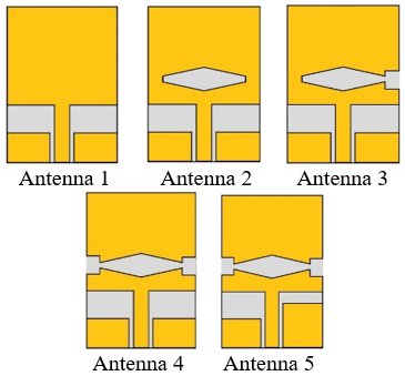
3.2 Design evolution
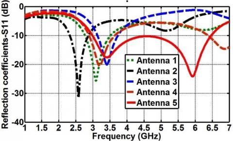
The design evolution of the suggested antenna is explained in detail as follows; four steps are useful for more explain the evolution of the suggested antenna as given in Figure 2. The results of the reflection coefficient S11 of antennas are depicted in Figure 3. Antenna 1 is an initial structure, that composes of a radiating element with a length (Lp) and a width (Wp). Figure 3 denotes that the bandwidth of the antenna 1 is ranging from 2.77 GHz to 3.52 GHz and the resonant frequency is around the 3.08 GHz.
Antenna 2 is obtained by using a hexagonal slot which is etching on the rectangular patch for extending the surface current on the patch and creates the miniaturization ability. The antenna 2 produces the bandwidth from 2.32 GHz to 2.87 GHz centered on 2.57 GHz.
Antenna 3 has been designed by inserting a rectangular notch in the radiating element for archive another band. It can be observed in Figure 3, that the antenna achieves a resonant frequency around 3.41 GHz and the impedance bandwidth for S11≤-10 dB is ranging from 3.13 GHz to 3.74 GHz.
Figure 2. The design evolution of the suggested antenna
Figure 3. Reflection coefficients of antennas
Antenna 4 has two rectangular notches at the end of the hexagonal slot; this structure offers two bands of operations and two resonant frequencies of 3.2 GHz, 6.77 GHz.
Antenna 5 is the final step; an asymmetric ground plane has been formed for enhancement of the upper bandwidth and get a good impedance matching. It can be noted from Figure 3, that a wide-band from 3 GHz to 6.46 GHz has been formed due to an asymmetric ground plane.
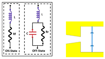
For covering triple-bands of operation with a single antenna, two PIN diodes have been used as shown in Figure 4. The Infineon bar PIN diode with a frequency range of 10 MHz to 6 GHz has been choices to integrate into the radiating element of the antenna to achieve the band reconfigurability ability [18]. According to ON/OFF states of diodes is can provide the switching operation bands. Both the ON/OFF states of the PIN diode have a correspondence circuit mode are indicated in Figure 4(a). The inductance value is L=1.8 nH for two OFF and ON states.
(a) ON and OFF states (b) PIN diode modeling in CST
Figure 4. Equivalent circuit of the PIN diode
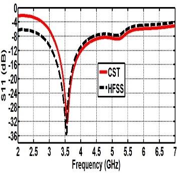
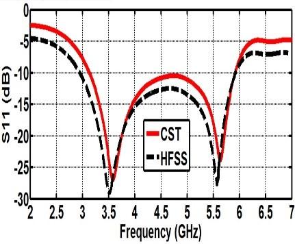
(a) Mode 1 (D1-ON, D2-ON)
(b) Mode 2 (D1-OFF, D2-ON)
(c) Mode 3 (D1-OFF, D2-OFF)
Figure 5. Reflection coefficients of the frequency reconfigurable patch antenna with a PIN diode in the ON and OFF states
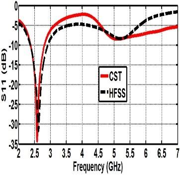
In case 1, the circuit model of the ON state of the PIN diode is a series combination between the resistance Rf=3 Ω and the inductance L. While in case 2 the circuit model when the PIN diode has the OFF state is a parallel composite of the capacitance C=0.15 pF and the resistance Rr=5 KΩ which are series between the inductance L. Moreover, the RLC circuit of the OFF-ON state of the diodes is modeled in the CST microwave studio software as shown in Figure 4(b). The positions of the PIN diodes (D1 and D2) are optimized to obtain the band reconfigurability and covering the requirements of the WiMAX/WLAN bands applications. The suggested antenna is simulated using the CST software and the obtained results are valeted using HFSS software. The suggested antenna is capable to operate in various modes that are controlled by the state of diodes (D1-D2). When D1 and D2 have the ON-state, and D1 has the ON-state and D1 has the OFF-state, D1 and D2 have OFF-state the suggested antenna is in the mode 1, mode 2, and mode 3 respectively. Figure 5 shows the reflection coefficient of the suggested antenna in several modes. The obtained results from the CST and HFSS software are agreed coherently.
In mode 1 the simulated impedance bandwidth for S11≤-10 dB is ranging from 2.36 GHz to 2.81 GHz with the resonant frequency of 2.58 GHz. While in mode 2 the suggested antenna offers the resonant frequency of 3.56 GHz and the bandwidth of 3.20-4.23 GHz. Whereas, in mode 3 the antenna archives a wide-band from 3.13 GHz to 5.92 GHz with two resonant frequencies of 3.58 GHz and 5.63 GHz.
Depending on two states of diodes the designed antenna can switch on three bands of operation which are covering the demand of WLAN at 2.45/5.2/5.8 GHz and WiMAX at 3.5/5.5 GHz.
Table 2 presents the simulation results of the proposed antenna in terms of bandwidth and resonant frequency for the achieved modes provided by both PIN diodes. Equation (9) was used in calculating the impedance bandwidth (BW-10 dB(%)), as given by [19]:
$B W=\left(\frac{f m a x-f m i n}{f r}\right)$ (9)
where, fr: resonant frequency, fmax: maximum frequency, fmin: minimum frequency, BW: Bandwidth.
Table 2. The possible modes with their corresponding operating bandwidths and frequencies
|
Configuration D1-D2 |
BW−10 dB (%), CST |
BW−10 dB (%), HFSS |
fr(GHz) CST |
fr(GHz) HFSS |
|
Mode 1 ON-ON |
17 |
17.6 |
2.58 |
2.62 |
|
Mode 2 OFF-ON |
29.5 |
30.4 |
3.56 |
3.54 |
|
Mode 2 OFF-OFF |
60 |
61 |
3.58 5.63 |
3.51 5.56 |
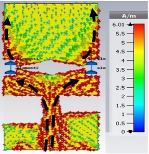
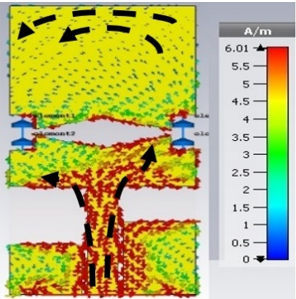
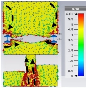
5.1 Current distribution
To explain the mechanism of the multi-band operation, the vector current distribution of the suggested antenna in different modes are presented in Figure 6. It can be noted that the PIN diodes control the current distributions on the main radiating element. these variations of the current distribution produce a different electrical length hence generates different resonance modes. At mode 1, the current flows towards a longer path hence increase the electrical length as depicted in Figure 6(a). In this case, the suggested antenna achieves a resonant frequency of 2.58 GHz in the lower band. whereas in mode 2, the current distribution is much stronger on the lower radiating element as indicated in Figure 6(b). As a consequence, the electrical length decreases, therefore the antenna produces a second band. In mode 3 as shown in Figure 6(b) the current distribution with different towards has been created on the radiator which archives different electrical lengths and this combination can provide two resonant frequencies of 3.58 GHz and 5.63 GHz.
Knowing that the optimized antenna offers three modes of operating, their path lengths corresponding to each resonant frequency (Fr1=2.58 GHz, Fr2=3.56 GHz,Fr3=5.63 GHz) are calculated from the surface current distributions for the given frequency modes as follows:
$P_{F r 1}=\left(\frac{\mathrm{Lf}}{2}+\frac{\mathrm{Wp}}{2}+\mathrm{Lp}\right)=33.25 \mathrm{mm}$ (10)
$P_{F r 2}=\left(\frac{\mathrm{Lf}}{2}+\frac{\mathrm{Wp}}{2}+\frac{\mathrm{Lp}}{4}\right)=20.25 \mathrm{mm}$ (11)
$P_{F r 3}=\left(\frac{\mathrm{Lf}}{2}+\frac{2 \mathrm{Lp}}{4}\right)=16 \mathrm{mm}$ (12)
These paths resonant lengths (PFr values) are calculated from the surface current distributions for the given frequency modes. These lengths are approximately equal to one-quarter of the guided wavelength is determined based on the following Eq. (13) [16].
$P_{f r}=\frac{C}{4 f_{r} \sqrt{\varepsilon_{\text {reff}}}}$ (13)
(a) Mode 1 at 2.58 GHz
(b) Mode 2 at 3.56 GHz
(c) Mode 3 at 5.63 GHz
Figure 6. Current surface distribution
5.2 Radiation patterns
In three modes, the radiation pattern of the suggested structure is omnidirectional in H-plane while it is bidirectional in E-plane as depicted in Figure 7. Besides that, this antenna has symmetric patterns due to its symmetric radiating element structure.
Figure 7. Simulated radiation patterns at various modes
The simulated gain and efficiency of the antenna over the band for the three switched states is observed in Figure 8. It shows that the maximum gain and efficiency values obtained at the resonant frequency in the mode 1, mode 2 and mode 3 are 1.48 dBi, 89.60%, 1.69 dBi, 87.14% and 1.89 dBi, 3.44 dBi, 90.48%, 81.57% respectively.
In addition, the size of the antenna is less than a half wavelength at the lower operating frequency. As a result, gain and efficiency affect.
Figure 8. Simulated gain and radiation efficiency for various modes
The performance of the suggested antenna is compared with several reconfigurable antennas observed in literature, which is tabulated in Table 3. It can be seen that the suggested reconfigurable antenna achieves the band reconfigurability by using only two switching PIN diodes, which minimize the complexity of biasing circuits and hence the distortion resulting from it. In addition, the suggested antenna has a compact size, which make it a suitable candidate for miniature wireless systems.
Table 3. Comparison of the suggested antenna performance
|
Ref. |
Dimension (mm3) |
No. Band |
No. of switches |
|
[20] |
80×80×1.6 |
2-3 |
4 |
|
[21] |
50×50×1.6 |
1 |
2 |
|
[9] |
48×48×3.2 |
2 |
4 |
|
[22] |
45×40×1.6 |
4 |
10 |
|
[23] |
40×40×1.6 |
3 |
1 |
|
[24] |
39×37×1.6 |
3 |
1 |
|
[25] |
35×40×1.6 |
3 |
1 |
|
[26] |
30×26×1.6 |
3 |
4 |
|
The suggested antenna |
31×14.5×1.6 |
3 |
2 |
A compact reconfigurable patch antenna has been suggested and investigated in this letter. The antenna contains the rectangular patch loaded with a hexagonal slot. Only two diodes are employed to offer a band reconfigurable property. According to the ON-OFF state of diodes, three bands are achieved, 2.36-2.81 GHz and 3.20-4.23 GHz and 3.13-5.92 GHz. The obtained results from CST and HFSS have a good agreement. In addition, suggested reconfigurable antenna has other performance, such as good radiation patterns, simple structure, small size which make it a capable candidate for wireless communication in diverse applications.
[1] Majid, H.A., Rahim, M.K.A., Hamid, M.R, Ismail, M.F. (2014). Frequency reconfigurable microstrip patch-slot antenna with directional radiation pattern. Progress in Electromagnetics Research, 144(4): 319-328. https://doi.org/10.2528/PIER13102901
[2] Bilgi, M.M., Yegin, K. (2013). Polarization reconfigurable patch antenna for wireless sensor network applications. International Journal of Distributed Sensor Networks, 61(2): 960-964. https://doi.org/10.1155/2013/967329
[3] Li, L., Wu, Z., Li, K., Yu, S., Wang, X., Li, T., Zhai, H. (2014). Frequency-reconfigurable quasi-Sierpinski antenna integrating with dual-band high-impedance surface. IEEE Transactions on Antennas and Propagation, 62(9): 4459-4467. https://doi.org/10.1109/TAP.2014.2331992
[4] Xiao, S., Zheng, C., Li, M., Xiong, J., Wang, B.Z. (2015). Varactor-loaded pattern reconfigurable array for wide-angle scanning with low gain fluctuation. IEEE Transactions on Antennas and Propagation, 63(5): 2364-2369. https://doi.org/10.1109/TAP.2015.2410311
[5] Cai, Y., Du, Z. (2009). A novel pattern reconfigurable antenna array for diversity systems. IEEE Antennas and Wireless Propagation Letters, 8: 1227-1230. https://doi.org/10.1109/LAWP.2009.2035720
[6] Brown, E.R. (1998). RF-MEMS switches for reconfigurable integrated circuits. IEEE Transactions on Microwave Theory and Techniques, 46(11): 1868-1880. https://doi.org/https://doi.org/10.1109/22.734501
[7] Kadam, R.S., Kulkarni, A. (2018). Radiation pattern of reconfigurable antenna design for portable device applications. Traitement du Signal, 35(2): 153-168. https://doi.org/10.3166/TS.35.153-168
[8] El Yassini, A., Ibnyaich, S., Chabaa, S., Zeroual, A. (2020). Miniaturized broadband‐multiband planar antenna with a symmetric quarter‐circular ground plane for WLAN/WiMAX standards. Microwave and Optical Technology Letters. https://doi.org/10.1002/mop.32402
[9] Reddy, V.V., Sarma, N.V.S.N. (2015). Circularly polarized frequency reconfigurable Koch antenna for GSM/Wi‐Fi applications. Microwave and Optical Technology Letters, 57(12): 2895-2898. https://doi.org/10.1002/mop.29463
[10] Trad, I.B., Rmili, H., Floch, J.M., Zouch, W., Drissi, M. (2015). Planar square multiband frequency reconfigurable microstrip fed antenna with quadratic Koch‐Island fractal slot for wireless devices. Microwave and Optical Technology Letters, 57(1): 207-212. https://doi.org/10.1002/mop.28815
[11] Kuo, Y.L., Wong, K.L. (2003). Printed double-T monopole antenna for 2.4/5.2 GHz dual-band WLAN operations. IEEE Transactions on Antennas and Propagation, 51(9): 2187-2192. https://doi.org/10.1109/TAP.2003.816391
[12] Sabapathy, T., Bashah, M.A., Jusoh, M., Soh, P.J., Kamarudin, M.R. (2016). Frequency reconfigurable rectangular antenna with T-slotted feed line. In 2016 International Conference on Radar, Antenna, Microwave, Electronics, and Telecommunications (ICRAMET), pp. 81-84. https://doi.org/10.1109/ICRAMET.2016.7849587
[13] Xin, G.L., Xu, J.P. (2007). Wideband miniature G-shaped antenna for dual-band WLAN applications. Electronics Letters, 43(24): 1330-1332. https://doi.org/10.1049/el:20072520
[14] Rasool, M., Farooq, R., Rashid, M.H., Zafar, A., Afzal, H., Alimgeer, K.S., Iftikhar, A. (2018). A compact open complementary split ring resonator inspired triband reconfigurable coplanar waveguide fed antenna. Microwave and Optical Technology Letters, 60(6): 1454-1459. https://doi.org/10.1002/mop.31190
[15] Saleh, A.A., Abdullah, A.S. (2014). A novel design of patch antenna loaded with complementary split-ring resonator and L-shape slot for (WiMAX/WLAN) applications. Int. J. Wireless and Microwave Technologies, 3: 16-25. https://doi.org/10.5815/ijwmt.2014.03.02
[16] Balanis, C.A. (2016). Antenna Theory: Analysis and Design. John Wiley and Sons, Hoboken, New Jersey.
[17] Ullah, S., Ahmad, S., Khan, B.A., Flint, J.A. (2018). A multi-band switchable antenna for Wi-Fi, 3G Advanced, WiMAX, and WLAN wireless applications. International Journal of Microwave and Wireless Technologies, 10(8): 1–7. https://doi.org/10.1017/S1759078718000776
[18] Infineon PIN diode Bar 50 Series: http://www.infineon.com/upload/Document/cmc_upload/documents/081/844/bar50series_1.pdf.
[19] Chaouche, Y.B., Messaoudene, I., Benmabrouk, I., Nedil, M., Bouttout, F. (2019). Compact coplanar waveguide-fed reconfigurable fractal antenna for switchable multiband systems. IET Microwaves, Antennas & Propagation, 13(1): 1-8. https://doi.org/10.1049/iet-map.2018.5005
[20] Choukiker, K.Y., Behera, S.K. (2016). Wideband frequency reconfigurable Koch snowflake fractal antenna. IET Microwaves, Antennas & Propagation, 3(1): 203-208. https://doi.org/10.1049/iet-map.2016.0238
[21] Jose, M.C., Chithra Devi, R., Sreeja, B.S., Meraline, S., Radha, S. (2019). A novel wideband pattern reconfigurable antenna using switchable parasitic stubs. Microwave and Optical Technology Letters, 61(4): 1090-1096. https://doi.org/10.1002/mop.31698
[22] Nafde, Y., Pande, R. (2017). Design and analysis of resistive series RF MEMS switches based fractal u-slot reconfigurable antenna. Wireless Personal Communications, 97(2): 2871-2886. https://doi.org/10.1007/s11277-017-4639-8
[23] Ullah, S., Hayat, S., Umar, A., Ali, U., Tahir, F.A., Flint, J.A. (2017). Design, fabrication and measurement of triple band frequency reconfigurable antennas for portable wireless communications. AEU-International Journal of Electronics and Communications, 81: 236-242. https://doi.org/10.1016/j.aeue.2017.07.028
[24] Iqbal, A., Ullah, S., Naeem, U., Basir, A., Ali, U. (2017). Design, fabrication and measurement of a compact, frequency reconfigurable, modified T-shape planar antenna for portable applications. Journal of Electrical Engineering and Technology, 12(4): 1611-1618. https://doi.org/10.5370/JEET.2017.12.4.1611
[25] Shah, I.A., Hayat, S., Khan, I., Alam, I., Ullah, S., Afridi, A. (2016). A compact, tri-band and 9-shape reconfigurable antenna for WiFi, WiMAX and WLAN applications. International Journal of Wireless and Microwave Technologies (IJWMT), 6(5): 45-53.
[26] Han, L., Cheng, G., Han, G., Zhang, W. (2019). Reconfigurable ultra‐wideband monopole antenna with single‐, dual‐, and triple‐band notched functions. International Journal of RF and Microwave Computer‐Aided Engineering, 29(9): e21837. https://doi.org/10.1002/mmce.21837