Anil Kumar Kurra* | Usha Rani Nelakuditi
OPEN ACCESS
For most cryptographic algorithms, the secret keys must be permanently stored in non-volatile memories (NVNs) and used for distinct security operations. This gives rise to power constraints, location limits and security threats to hardware facilities. To solve the problems, this paper proposes a novel and reliable current starved inverter (CSI) based on a physical unclonable function (PUF) architecture (8, 16 and 32 stages), using 45nm complementary metal-oxide-semiconductor (CMOS) technology. The proposed CSI was simulated on Spectre Simulation Platform. The results show that its uniqueness, reliability and randomness were 49.26 %, 98.86 % and 86.12 %, respectively, in the temperature range of -20~80 ℃. In addition, the performance of the proposed CSI was proved to outshine that of existing PUF architectures in stability and reliability. The research results are significant for the development of critical security applications.
current starved inverter (CSI), cryptographic keys, physical unclonable functions (PUFs), support vector machine (SVM), temperature instability
The drastically increasing of smart devices over the past decade, these devices are strong influences our day to day life and found in a home, cars, workplaces, etc. Now a day's People are strongly relying on electronic devices to perform sensitive tasks such as electronic payments, tag applications, etc. However, on numerous occasions, a wide verity of privacy and security related attacks are held over these electronic devices to steal valuable information. The traditional private key based-cryptographic paradigms are very hard to embed into resource-constrained digital devices and it requires Non-Volatile Memories (NVM) to store secret keys, as well as consumes more power. However, on-chip NVM prone to invasive, semi-invasive, and physical attacks. Therefore, which are not suitable for resource-constrained intensive applications. Hence to address above mentioned problems, to enhance the trustworthiness of the electronic devices, silicon Physical Unclonable Functions (PUFs) are emerged to be one of the cost-effective and power-efficient cryptographic primitive, which can be widely used to generate hardware cryptographic keys without using hashing and Finally the obtained keys are used for device authentication, identification, secret key generation.
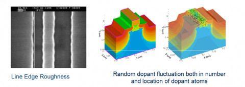
Figure 1. Random dopant fluctuation in number
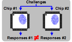
The concept of PUFs has been first proposed by Pappu [1-3] to provide the desired level of security with a low area overhead. PUF is a disordered physical entity by utilizing the uncontrollable tiny process variations during the fabrication process produces a unique set of secure keys. The minute and uncontrollable fabrication mismatches make each IC is individual from the same wafer (as shown in Figures 1 & 2) and which can be detected by using the sensing circuits (whose having multiple interconnects and devices). The type of mismatches that occurred in each circuit can be divided into two types, such as global mismatches and local mismatches. Global mismatches occur during the fabrication of ICs, which is unavoidable and uncontrollable. On the other hand, local mismatches are inherent and depend on voltage (V) and temperature (T), respectively. PUF response is always a characteristic function of Integrated Circuit (IC) and not possible to clone the exact device with the same characteristics. Mathematically, PUFs are irreversible (one way) probabilistic challenge (Ci)-response (Ri) functions and can be expressed by (1). Due to the physical properties of a PUF, each set of a challenge can results/triggers the different set of response bits at each PUF instance and cannot be measured until the IC is integrated. The stored on chip physical parameters leads to remarkable security advantages and More importantly, behavior of each PUF should be dynamic and unique nature.
$\mathrm{PUF}=\mathrm{C}_{\mathrm{i}} \leftarrow \mathrm{R}_{\mathrm{i}}: \forall_{\mathrm{i}} \leftarrow[0,1]^{*}$ (1)
Figure 2. CRP behavior of ICs
In an abstract sense, architectures of the PUFs come in different flavors. Depending upon the nature of CRPs, PUFs can be broadly classified into strong PUFs and weak PUFs, respectively. Strong PUFs are class of PUFs, which have an exponential number of CRPs with respect to the number of physical stages and a strong relation between input and output. Hence the adversary cannot enumerate the CRPs with a fixed amount of time, and obtained responses are stable over the wide range of the temperatures. Strong PUFs are arbiter PUFs [4-6], ring oscillator PUFs [7, 8], etc. On the other hand, weak PUFs are PUFs have limited number of CRPs and whose responses strongly depend on manufacturing variability's and least susceptible to presented modelling attacks. Weak PUFs are SRAM PUFs, butterfly PUFs, etc. Even though many numbers of PUF architectures have been proposed still Reliability is one of the common problems for all types of PUFs. The response generated from the PUF is unreliable because factors like temperature (T), supply voltage (VDD), aging phenomenon, and noise can lead to flip the output response temporarily. Unlike the environmental conditions of the device, aging is also an important phenomenon that permanently alters the response of the PUF. The primary aging mechanisms mainly caused due to Negative Bias Temperature Instability (NBTI), Hot Carrier Injection (HCI), Time-Dependent Dielectric Breakdown (TDDB) and electromigration [9-10]. In this paper, we investigated the design of delay-based strong PUFs in 45-nm complementary metal-oxide-semiconductor (CMOS) technologies targeting low-power security applications. In contrast to the above works, this paper presents a novel, reliable, and efficient Current Starved Inverter (CSI) based arbiter PUF circuit for device authentication.
The main contributions of the paper include, Estimated the security metrics of the PUF architecture such as uniqueness, reliability, and randomness. Measured the reliability of CSI PUF architecture from the perspective of voltage and temperature. The experimental results show that the proposed architecture technique allows the generation of larger and updated challenge-response pairs (CRP space) compared with existed arbiter PUF architectures. The rest of the paper is organized as follows: In section 2 introduces the background and motivation of the work as well as conventional and feed-forward arbiter PUFs with their limitations. Section 3 describes the proposed CSI based PUF architecture and its operation, Section 4 provides proposed PUF architecture performance evaluation based on security metrics and finally, section 5 concludes the paper.
Reliability is one of the major problems addressed in various PUF applications. Since PUF outputs mainly depend on mismatches and different parameters of the PUF structures, hence generated signatures from each PUF can be vulnerable to the noisy and temporal variations can leads to flip the final response. Therefore, to enhance the reliability of PUFs, several architectures have been proposed in literature survey [5, 6] at different levels such as system level, model level, and circuit level. Prior work has been done to improve the reliability of arbiter PUFs using conventional methods, including Error correction codes (ECC) or fuzzy extractors, to correct the flipped responses. In fact the implementation cost and hardware area overhead relatively high as compared to the proposed architectures, which occupies more space and dissipates the power. Besides, using ECC or fuzzy extractors have been already discussed in the literature [11].
Even a wide verity of strong PUFs, we are mainly focused on the arbiter based PUFs due to its large number of CRP databases and complex architecture. The basic concept of arbiter PUFs was first demonstrated in 2002 [4, 5]. Whose response was always measured in terms of the timing difference between two signals. The current open problem for arbiter PUFs were susceptible to modeling attacks and reliability. Gassend et al. successfully predicted the arbiter response using standard Machine Learning (ML) methods, such as support vector machine (SVM) and perceptrons method by collecting a large number of CRPs [12-14]. Therefore the attacker can easily clone the PUF architecture. To make more secure, proposed a feed-forward PUF [15], in this case, arbiters were placed at the middle of the arbiter PUF, which will acts as a challenge bit for the further stages and improves the security by introducing non-linearity's as the multiple number of arbiters leads to degrade the reliability of the PUF. Hence, to further enhance the reliability, proposed a several novel non-linear arbiter PUF configurations, such as modified arbiter PUFs, logic reconfigurable feed-forward arbiter PUFs [15], mux/demux PUF [16], XOR arbiter PUF [17], tristate arbiter PUF [5], etc. The all proposed arbiter PUFs are still suffering the reliable issues and also different types of modeling attacks. Hence to combat the above-mentioned issues and also to reduce the circuit complexity proposed a novel Current Starved Inverter (CSI) based PUF architecture.
2.1 Working principle of arbiter PUF
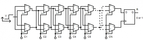
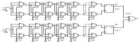
Arbiter PUF is one of the most popular delay-based PUF. Multiplexer (MUX) is a fundamental building block (switching element) of the arbiter PUFs. Figure 3 illustrates the conventional architecture of the N-bit arbiter PUF. It consists of N number of multiplexers are connected in a row with each other and an arbiter at final stage of the delay network. Each stage of the delay network is composed of two MUXs connected at top and bottom, respectively. The selection line of each MUX will act as a challenge by utilizing the intrinsic process variations and crates the small random delay difference on each stage. The arbiter acts as a decision element which decides the final response by comparing the analogy timing difference between two signals and produces the digital value with the help of the sensing circuit. If the top input of the arbiter arrives earlier than bottom input, then the output will be one otherwise, the output will be considered as a zero. The final response always depends on the applied challenges and electrical behavior of the chip. The set of challenges and corresponding responses are termed to be (CRP), which triggers the use of authentication mechanisms. Since collecting the large set of a database (CRP pairs) necessary to analyze the behavior of the arbiter PUF.
Figure 3. Schematic of the linear N-stage arbiter PUF
2.2 Mathematical model of arbiter PUF
The functionality of an arbiter PUF can be described with the help of the additive linear delay model [18-20]. The overall delays of the signals are modelled by summing the individual delays of each stage. The final delay difference ($\Delta i$) is the delay difference between upper and lower paths at the ith stage can be expressed as (2) and corresponding run time delay at each stage could be either crossed (1) or uncrossed (0) respectively.
$\Delta \mathrm{i}=\left\{\begin{array}{ll}{\Delta_{\mathrm{i}-1}+\delta_{\mathrm{i}}^{1},} & {\text { if } \mathrm{c}_{\mathrm{i}}=1} \\ {-\Delta_{\mathrm{i}-1}+\delta_{\mathrm{i}}^{\theta},} & {\text { if }\mathrm{c}_{\mathrm{i}}=0}\end{array} \text { for } \mathrm{i}=1,2,3 \ldots \mathrm{n}\right.$ (2)
where, $\Delta_{0}=0$ and $\mathrm{C}=\left(\mathrm{c}_{1}, \mathrm{c}_{2}, \mathrm{c}_{3} \ldots, \mathrm{c}_{\mathrm{n}}\right) \in\{0,1\}^{\mathrm{n}}$ is the challenge vector and n represents the number of stages in the Arbiter PUF. The cumulative sum of delay of the nth stage can expressed as (3)
$\Delta_{\mathrm{n}}=\emptyset^{\mathrm{T}} \cdot \mathrm{D}$ (3)
where, $\emptyset$ represents the feature vector expressed as $\emptyset=\left(\emptyset_{1}, \emptyset_{2}, \ldots . \emptyset_{n+1}\right)^{\mathrm{T}} \in\{-1,1\}^{\mathrm{n}+1}$ and $\mathrm{D}=\left(\mathrm{d}_{1}, \mathrm{d}_{2} \ldots \mathrm{d}_{\mathrm{n}+1}\right) \in \mathrm{R}^{\mathrm{n}+1}$ as weight vector respectively. ith the stage of the feature vector holds the challenge bit string (6) and its individual stages represents the Eqns. (4), (5) and (6), respectively.
$\emptyset_{i}=\emptyset_{i}(C)=\prod_{j=1}^{n}\left(2 C_{j}-1\right),$ for ${i}=1,2,3 \ldots, n, \emptyset_{n+1}=1$
where,
$\mathrm{d}_{\mathrm{i}}=\frac{\delta_{\mathrm{i}-1}^{0}+\delta_{\mathrm{i}-1}^{1}+\delta_{\mathrm{i}}^{0}-\delta_{\mathrm{i}}^{0}}{2},$ for $\mathrm{i}=2,3, \ldots, \mathrm{n}$ (4)
$\mathrm{d}_{1}=\frac{\delta_{1}^{0} - \delta_{1}^{0}}{2}$ (5)
$\mathrm{d}_{\mathrm{n}+1}=\frac{\delta_{\mathrm{n}}^{0}+\delta_{\mathrm{n}}^{1}}{2}$ (6)
The final response bit is determined by arbiter, comparing the its delay paths and which path is faster, i.e. where $\Delta_{n}$ is positive or negative (7)
$\mathrm{r}=\left\{\begin{array}{c}{1, \& \emptyset^{\mathrm{T}} \mathrm{D}>0} \\ {-1, \& \text { otherwise }}\end{array}\right.$ (7)
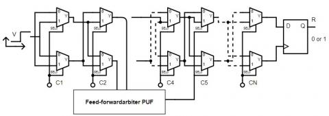
Lim accurately formulated the linear additive delay model for arbiter PUF as well as memiristor crossbar PUF by using the optimization- theoretic approach. The attackers can derive a liner homogeneous system by collecting a group of CRPs and which forms a polytope in the space of vector. Hence to enhance the unpredictability of the arbiter PUFs and to resist the attacks over the machine learning attacks, proposed a set of non-liner PUFs such as feed-forward arbiter PUFs, feed forward MUX PUF overlap structure, feed-forward MUX PUF cascade structure etc. [20]. Figure 4 depicts the basic architecture of the feed-forward arbiter PUF. To avoid linearity inserted an arbiter circuit in middle of the main path. Hence the delay can be depending on one more additional arbiter PUFs. These structures significantly resistance the modelling attacks but the reliability of the PUF has been effected due to the environmental variations. To achieve the unpredictability and reliability proposed a XOR arbiter PUFs. The XOR arbiter PUF is composed of a several independent conventional arbiter PUFs and an XOR gate respectively. And Figure 5 shows the two stage architecture of the XOR arbiter PUF. The final response of the XOR gate is dependents upon applied individual challenges and delays of two arbiters.
Figure 4. Feed-forward arbiter PUF architecture
Figure 5. XOR arbiter PUF architecture
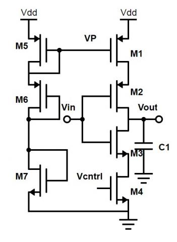
As per the literature survey authors have designed the several types of arbiter PUF architectures by choosing the delay element (switching element) as inverters, multiplexer, tristate buffer, xor gate etc. to design the delay network [20-21]. First time we are designed the delay network using the DPDE such as Current starved inverter (CSI) element by taking non-linearity's into consideration [22], to enhance the metrics of the PUF circuit. CSI is core of the arbiter PUF architecture, which acts like a switch and controls the delay characteristics of the PUF circuit. More specifically variable delay elements mainly employed in low power applications like Digital Delay Locked Loops (DDLL) [23], Digital Controlled Oscillators (DCO) [24], Phase Locked Loops (PLL) [25], Duty Cycle Converter (DCC) [26], Pulse Width Controlled Loops (PWCL), microprocessors, microcontrollers and also one of the essential building block in System-on-chip (SOC). The majority of the delay lines are designed to operate accurately synchronization among the different digital blocks. There are three different types of techniques have been proposed to design the variable delay elements such as shunt capacitor delay element [27, 28], current starved delay element and variable resistor based delay element respectively. Shunt capacitor delay element occupies the large silicon area and suffers from narrow tuning range. On the other hand, variable resistor based delay element requires PMOS stack transistors to vary the falling edge of the output and NMOS stack transistors to vary the delay of the rising edge of the output. Hence to achieve the better performance proposed a modified CSI variable delay element based arbiter PUF architecture and XOR gate chosen as an arbiter to detect the final response of the delay network. Figure 6 shows the proposed CSI delay element and seven transistor XOR gate respectively.
Figure 6. Proposed reliable current starved inverter
The proposed CSI consists of total seven transistors, M2 and M3 will acts as the inverter which indirectly controls the charging and discharging current Ic of the output load capacitance. Transistors M1 and M4 regulates the delay of the whole circuit through Vp and Vcntrl respectively. The extra added transistors (M5, M6 and M7) to the regular inverter makes dominates the threshold voltage which controls the mobility and counter attacks the negative temperature coefficient. As the temperature are increases beyond the certain limit it is going to effect on performance of the circuit (delay, power). Hence to achieve this phenomenon we added an extra transistor to the current starved inverter there by which effectively controls the voltages of Vp and Vcntrl. The propagation delay of each stage can be calculated Eq. 8
$\mathrm{t}_{\mathrm{d}}=\frac{\mathrm{C}_{0} \mathrm{V}_{\mathrm{dd}}}{\eta \mathrm{I}_{\mathrm{D}}}$ (8)
where, $\mathrm{C}_{0}$ represent the total load capacitance, $\mathrm{V}_{\mathrm{dd}}$ is the total power supply, $\eta I_{D}$ is the mean current ( $I_D$ =saturation current and $\eta$ fixed parameter for a given inverter). the drain current equation can be expressed by Eq. 9.
$\mathrm{I}_{\mathrm{D}}=\frac{\mu \mathrm{C}_{\mathrm{OX}} \mathrm{W}}{2 \mathrm{L}}\left(\mathrm{V}_{\mathrm{GS}-} \mathrm{V}_{\mathrm{t}}\right)^{2}$ (9)
where, $\mu, \mathrm{C}_{\mathrm{OX}}$,W,Vt,L and VGS are the carrier mobility, gate capacitance, effective channel width, threshold voltage, channel length and gate to source voltage, respectively. from the above expressions are temperature parameters $V_{t}$ and $\boldsymbol{\mu}$ can be expressed as Eqns. 10 and 11 respectively.
$\mathrm{V}_{\mathrm{t}}(\mathrm{T})=\mathrm{V}_{\mathrm{t}}\left(\mathrm{T}_{0}\right)-\sigma\left(\mathrm{T}-\mathrm{T}_{0}\right)$ (10)
$\mu(\mathrm{T})=\mu\left(\mathrm{T}_{0}\right)\left(\frac{\mathrm{T}}{\mathrm{T}_{0}}\right)^{\mathrm{K}}$ (11)
where, $\mathrm{T}_{0}$ is the refernce temperature and the temperature coefficient from the range of the 1.2 to 2 k respectively and $V_{t}$ range from 0.5-3mv/k. As threshold voltage is increases with decreasing temperature, resulting saturation current is increases. On the other hand charge carriers are increases with decreasing temperature, which in turn increases the drain saturation current. Hence the delay of regular inverter exhibits an overall positive temperature dependent relation.
3.1 Operation of the DPDE Based Arbiter PUF Architecture
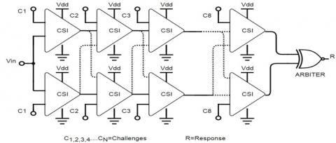
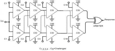
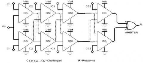
The proposed 8, 16 and 32 stage CSI arbiter PUF as shown in Figures 7, 8 and 9. Each stage introduces a fixed amount of time delay and its Delay can be altered non-linearly without introducing any external arbiters at the middle of the architecture and this can be varied mainly due to variations of the voltage at each and every individual stage. The architecture consist of two CSI elements at top and bottom stage and an input pulse signal is given to the two parallel connected CSI inverters and applied control voltage can acts as the challenge for the each and every stage. Due to applied input and control voltage results leads to variations in the final response and it can be detected by using the arbiter (XOR) respectively. As long as the number of delay stages are varied delay can be varied.
Figure 7. 8 stage CSI based arbiter PUF
Figure 8. 16 stage CSI based arbiter PUF
Figure 9. 32 stage CSI based arbiter PUF
3.2 Monte Carlo-based design analysis
The PUF design is strongly relies on the device process variations. To predict the random process variations of CMOS PUF design can be done using the statistical analysis. Here we performed a Monte-Carlo (MC) simulation, to determine PUF design parameters with respect to Gaussian distribution to assess the performance of the circuit effectively under different working conditions. Each MC iteration in the PUF design represents one PUF instance with unique variations. Large number of iterations were performed to collect the huge amount of statistical data to estimate security metrics of a PUF accurately and precisely. To target the low power security applications, we have performed comprehensive design analysis under different process nodes.
3.3 Simulation setup
The Proposed PUF design simulations were carried out cadence virtuoso CMOS 45nm process technology, whose nominal supply voltages range chosen to be 0.8V to 1.2V respectively. Applied the 200 iterations using MC analysis for a PUF circuit to extract the CRPs and to simplify the variation model, we estimated the process variations of PUF design under different voltage ranges and observed the effect of the variations with respect to three sigma plots (mean &standard deviation). Using the MC analysis we can differ the slight variations of PUF characteristics and MC analysis can be performed for the each and every circuit before they sent to the foundry to estimate the yield. Yield can be enhanced by each and every PUF circuit by making necessary design modifications to meet the required target. Obtained values represents the actual variations of the silicon since process variations mitigates on different levels of the design. Since scaling down the technology being effectively enhances the process parameters.
3.4 Statistical metrics for PUF performance
3.4.1 Uniqueness
Uniqueness is a quantitative index to distinguish the total number of PUF responses produced by different instances. Average Inter-chip Hamming Distance (HDAvg) used to evaluate the uniqueness of a specific PUF design to assess the PUF responses easily over the K different devices. Ideally, the normalized HDAvg of a PUF design should be 50 %. If the responses of a two PUF instances compared with same challenge, it implies that half of the response bits are different between each other. The uniqueness U mathematically expressed by Eq. 12.
uniquness (U) $=\frac{2}{\mathrm{K}(\mathrm{K}-1)} \sum_{\mathrm{K}}^{\mathrm{K}-1} \sum_{\mathrm{j}=\mathrm{i}+1}^{\mathrm{K}} \frac{\mathrm{HD}\left(\mathrm{R}_{\mathrm{i}} \mathrm{R}_{\mathrm{j}}\right)}{\mathrm{N}} \times 100$ (12)
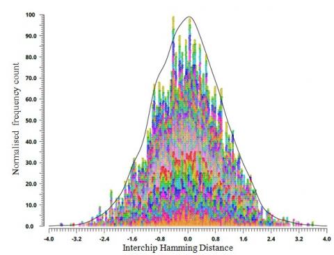
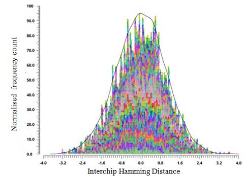
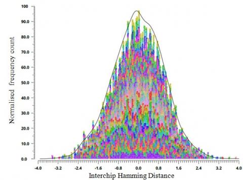
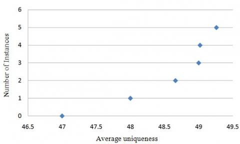
Let Ri and Rj be n-bit responses of two different chips i and j, to the same input challenge 'C' and N indicates the total number of PUF instances, respectively. To demonstrate the uniqueness of a proposed CSI PUF designs (8, 16 and 32 bit), were measured at different instances of PUF using CMOS 45nm technology models. Applied a set of 50 random challenges with 200 number of samples, at each and every iteration and whose responses were extracted using Monte-Carlo analysis. The distribution of the measured maximum Inter-chip HDAvg shown by Figures 10(a), 10(b) and 10(c) at different delay stages (8, 16 and 32 stages), respectively. Therefore the uniqueness to be calculated from 50 instances of the PUF by averaging its mean value at an ambient temperature of 270c.The obtained uniqueness should be close to ideal value (50 %) μ= 49.26 % (shown in Figure 10(d)). It indicates that aspects ratio and delay stages which significantly impact on the performance of the Inter-chip HDAvg of the PUF design.
(a)
(b)
(c)
(d)
Figure 10. Frequency distribution of measured 45 nm CMOS CSI arbiter PUF(a)8-stage(b)16-stage (c) 32 stage (d) Average uniqueness of CSI arbiter PUF
3.4.2 Reliability
It is an estimation of Bit Error Rate (BER) of a PUF response when the same challenge being applied to the PUF instance under different environmental conditions like temperature, supply voltage variations, etc. It can be calculated using Intra-Chip Hamming Distance (HDintra). Ideally, for a given PUF circuit implemented on any device, it should be perfectly recreated its output whenever it is queried with the challenge. Therefore, for device i, its reliability is can be evaluated by average intra-chip HD of s response samples, Ri', taken at reference operating condition for an N-bit response. The average intra-chip HD is calculated by (13)
$\mathrm{HD}_{\text {intra }}=\frac{1}{\mathrm{s}} \sum_{\mathrm{t}=1}^{\mathrm{s}} \frac{\mathrm{HD}\left(\mathrm{R}_{\mathrm{i}, \mathrm{R}_{\mathrm{i}, \mathrm{t}}}\right)}{\mathrm{N}} \times 100$ (13)
where, R(i, t)' is the tth sample of Ri'. The percentage figure of merit for reliability can be defined as
Reliability = 100-Hdintra
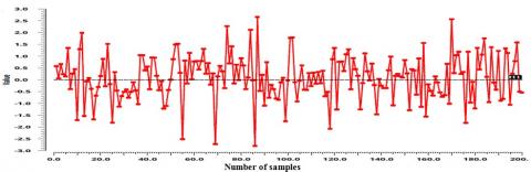
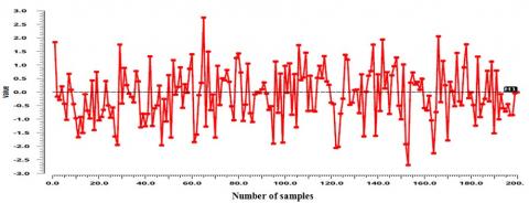
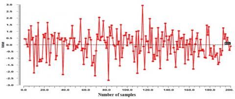
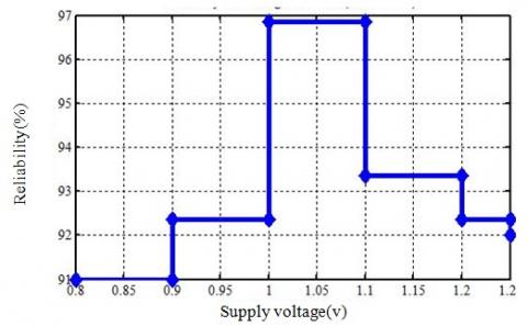
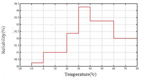
In order to estimate the reliability of the PUF, chosen 50 random number of challenges and measured its response at 1V and 270c as reference temperature, and collected set of challenges being measured by varying the temperature from -200c to 800c and estimated total number of bits to be flipped. As the CSI being produces the stable set of response bits and whose response were accurately estimated by using the soft response technique by keeping the threshold limit to distinguish the number of '0's and '1's in a given set of the response. It is evident that the proposed 32 bit CSI based PUF architecture with stands the wide range of the temperature and whose reliability is reaches to the ideal value 96.86 % and worst case reliability is 90% respectively. In the similar passion reliability of the PUF has effect on supply voltage variations, hence impact of the supply voltage was measured by changing the voltage range from 0.8v to 1.2v respectively. Figures 11 and 12 depicts the average reliability of CSI PUF against temperature and supply voltage. If the level of the reliability being degraded enormously such that it can be rectified by adapting low-overhead techniques. But this protocol violates the physical nature of the PUF and effects the area of the design.
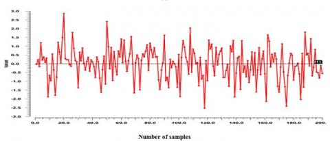
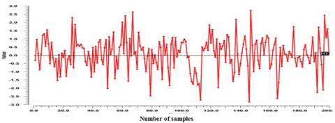
To estimate stability of the PUF responses applied a threshold limit to classify the stable '0' and stable '1'. The threshold limit should be taken in terms of a intervals such as (0~3.0) for '1' and (0~-3.0) chosen to be a '0' respectively. To evaluate number of '0' and '1's applied the random set of challenges and whose responses were measured based on the distribution of samples over the sample space. Initially measured the reliability of PUF instance at 270c as a reference temperature and applied the 200 number of samples by the keeping the measured response as constant 11(a) and varied the temperature dynamically as shown in Figures 11(b), 11(c), 11(d) and 11(e) respectively. From the obtained results measured average Intra-die hamming distance reaches the ideal value (96.86 %). The overall reliability of 32-stage CSI inverter PUF with respect to voltage and temperature shown by Figures 12 and 13, respectively.
(a)
(b)
(c)
(d)
(e)
Figure 11. Measurement of reliability with respect to temperature (a) 270c(b) 300c(c) 400c(d) 500c(e) 600c
Figure 12. Reliability Vs. Supply voltage variations
Figure 13. Reliability Vs. Temperature (℃)
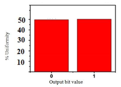
3.4.3 Uniformity
It can be used to measures the distribution of '0's and '1's in a given response of a PUF. Ideally, for each PUF, the response should contain equal proportion of '0's and '1's. The ideal value of uniformity is 50 %. Obviously, the challenge randomization module does not affect the uniformity of the arbiter PUF, since it only changes the challenges input to the arbiter PUF without affecting its delay characteristics. The uniformity of the ith PUF instance can be expressed by [14].
uniformity $=\frac{1}{\mathrm{n}} \sum_{\mathrm{i}=1}^{\mathrm{n}} \mathrm{R}_{\mathrm{i}, 1} \times 100 \%$ (14)
Let $R_{i, l}$ measures the lth bit from PUF instance-i. As far as challenge is kept constant, uniformity should be constant. Its uniformity can be obtained by averaging the all PUF instances of a given type.
Figure 14 depicts the average uniformity of the 32-stage CSI based PUF architecture for the 50 instances over 200 iterations and its uniformity should be 43.16 % respectively. Table 1 indicates the performance comparison of various types of PUFs with respect to technology aspect and Table 2 represents security metrics comparison arbiter PUFs with proposed CSI based PUF, respectively.
Figure 14. Estimation of uniformity (% '0' and '1')
Table 1. Performance comparison of various PUF implementations (*-simulation results)
|
|
[8]* |
[1] |
[11] |
Proposed work* |
|
|
PUF type |
Current mirror |
Ring oscillator |
SRAM |
CSI |
|
|
Process(nm) |
180 |
65 |
65 |
45 |
|
|
Architecture |
Analog |
digital |
analog |
digital |
|
|
Typical conditions |
Temperature(0c) |
-20~150 |
-40~120 |
-20~85 |
-20~80 |
|
Supply voltage(v) |
1.62~1.98 |
1.17~1.23 |
1.0~1.4 |
0.8~1.2 |
|
Table 2. Performance comparison of various arbiter PUFs
|
PUF type |
Uniqueness (%) |
Reliability (%) |
Randomness (%) |
|
Original mux |
44.2 |
94.20 |
65.50 |
|
Feed forward overlap |
47.5 |
91.30 |
77.6 |
|
Feed forward separate |
48.75 |
89.30 |
84.2 |
|
Feed forward cascade |
48.1 |
90.10 |
80.6 |
|
Mux-Demux |
41.9 |
92.90 |
59.6 |
|
CSI based PUF |
49.26 |
96.86 |
86.12 |
Over the past decade, PUFs provide a promising solution to many hardware problems such as counterfeiting, device authentication, and identification, etc. Transistor-based design provides a larger freewheel to the designer as compared to semi-custom design and enhances the process variations. The security metrics of PUF can be achieved more authentically after the fabrication of PUF circuits. In this paper, we have investigated the novel CMOS CSI based arbiter PUF were more area-efficient as compared to the existing arbiter PUFs, enhanced the security metrics like uniqueness and reliability. Hence the proposed PUF has chosen to be the best alternative for other PUFs and deserve for security application. Our future work directs towards the fabrication of the proposed PUF and designs a security protocol using proposed PUF.
[1] Gassend, B., Clarke, D., Dijk, M.V., Devadas, S. (2002). Silicon physical unclonable functions. the 9th ACM Conference on Computer and Communications Security, pp. 148-160. https://doi.org/10.1145/586110.586132
[2] Pappu, R., Recht, B., Taylor, J., Gershenfeld, N. (2002). Physical one-way functions. Science, 297(5589): 2026-2026. https://doi.org/10.1126/science.1074376
[3] Gassend, B., Clarke, D., Dijk, M.V., Devadas, S. (2002). Controlled physical unclonable functions. Computer Security Application Conference, Las Vegas, NV, USA, pp. 149-160. https://doi.org/10.1109/CSAC.2002.1176287
[4] Jouini, Z.C., Danger, J., Bossuet, L. (2011). Performance evaluation of physically unclonable function by delay statistics. Proc. IEEE 9th Int. NEWCAS, Bordeaux, France, pp. 482-485. https://doi.org/ 0.1109/NEWCAS.2011.5981324
[5] Tariguliyev, Z., Ors, B. (2012). Reliability and security of arbiter-based physical unclonable function circuits. International. Journal of Communication Systems, 26(6): 757-769. https://doi.org/10.1002/dac.2411
[6] Hori, Y., Yoshida, T., Katashita, T., Satoh, A. (2010). Quantitative and statistical performance evaluation of arbiter physical unclonable functions on FPGAs. 2010 International Conference on Reconfigurable Computing and FPGAs, Quintana Roo, Mexico, pp. 298-303. https://doi.org/10.1109/ReConFig.2010.24
[7] Maiti, A., Casarona, J., McHale, L., Schaumont, P. (2010). A large scale characterization of RO-PUF. Proc. IEEE Int. Symp. HOST, Anaheim, CA, USA, pp. 94-99. https://doi.org/10.1109/HST.2010.5513108
[8] Maes, R., Tuyls, P., Verbauwhede, I. (2008). Statistical analysis of silicon PUF responses for device identification. Proc. SECSI Workshop.
[9] Kufluoglu, Z., Alam, M.A. (2004). A computational model of NBTI and hot carrier injection time exponents for MOSFET reliability. Comput. Electron, 3(3-4): 165-169. https://doi.org/10.1007/s10825-004-7038-9
[10] Zafar, S., Kim, Y.H., Cabral, C., Paruchuri, V., Doris, B., Stathis, J., Callegari, A., Chudzik, M. (2006). A comparative study of NBTI and PBTI (charge trapping) in SiO2/HfO2 stacks with FUSI, TiN, Regates. in: Symposium on VLSI Tech-nology, Digestof Technical Papers, pp. 23-25. https://doi.org/10.1109/IWCE.2004.1407302
[11] Maes, R., Herrewege, A.V., Verbauwhede, I. (2012). PUFKY: A fully functional PUF-based cryptographic key generator. In Proc. Int. Workshop Cryptographic Hardware and Embedded Syst. (CHES’12), Leuven, Belgium, pp. 302-319. https://doi.org/10.1007/978-3-642-33027-8_18
[12] Ruhrmair, U., Sehnke, F., Solter, J., Dror, G., Devadas, S., Schmidhuber, J. (2010). Modeling attacks on physical unclonable functions. Proceedings of the ACM Conference on Computer and Communications Security, ser. CCS ’10, pp. 237-249. https://doi.org/10.1145/1866307.1866335
[13] Delvaux, J., Verbauwhede, I. (2013). Side channel modeling attacks on 65nm arbiter PUFs exploiting CMOS device noise. IEEE International Symposium on Hardware-Oriented Security and Trust. IEEE, pp. 137-142. https://doi.org/10.1109/HST.2013.6581579
[14] Lao, Y., Parhi, K.K. (2014). Statistical analysis of MUX-based physical Unclonable functions. IEEE Transactions on Computer-Aided Design of Integrated Circuits and Systems, 33(5): 649-662. https://doi.org/10.1109/TCAD.2013.2296525
[15] Majzoobi, M., Koushanfar, F., Potkonjak, M. (2008). Lightweight secure PUFs. in Proceedings of the 2008 IEEE/ACM International Conference on Computer-Aided Design, pp. 670-673. https://doi.org/10.1109/ICCAD.2008.4681648
[16] Lao, Y., Parhi, K.K. (2011). Novel reconfigurable silicon physical unclonable functions. Proc. Workshop FDSCPS, pp. 30-36. https://doi.org/10.1109/EIT.2011.5978614
[17] Becker, G.T., Kumar, R. (2014). Active and passive side-channel attacks on delay based PUF designs. IACR Cryptology Print Archive, 2014: 287-287. https://eprint.iacr.org/2014/287
[18] Lao, Y. Parhi, K.K. (2011). Reconfigurable architectures for silicon physical unclonable functions. Proc. IEEE Int. Conf. Electro Inf. Technol, pp. 1-7. https://doi.org/10.1109/EIT.2011.5978614
[19] Chang, H., Sapatnekar, S. (2003). Statistical timing analysis considering spatial correlation in a pert-like traversal. Proc. IEEE Int. Conf. Computer Aided Design Integr. Circuits Syst, pp. 621-625. https://doi.org/10.1109/ICCAD.2003.159746
[20] Lu, C.T., Hsieh H.H., Lu, L.H. (2009). A 0.6 V low-power wide- range delay-locked loop in 0.18 um CMOS. IEEE Microwave and Wireless Component Letters, 19(10): 662-664. https://doi.org/10.1109/LMWC.2009.2029752
[21] Wu, G., Deyuan, G., Tingcun, W., Christine, H.G., Hu, Y. (2009). A high-resolution multi-channel time-to-digital converter (TDC) for high-energy physics and biomedical imaging applications. 4th IEEE Conference on Industrial Electronics and Applications, 1133-1138. https://doi.org/10.1109/ICIEA.2009.5138334
[22] Han, S.R., Iuan, S. (2005). A single-path pulse width control loop with a built-in delay-locked-loop. IEEE Journal of Solid-State Circuits (JSSC), 40(5): 1130-1135. https://doi.org/10.1109/JSSC.2005.845988
[23] Panigrahi, J.K., Acharya, D.P. (2010). Performance analysis and design of wideband CMOS voltage controlled ring oscillator. IEEE International Conference on Industrial and Information Systems (ICIIS), 234-238. https://doi.org/10.1109/ICIINFS.2010.5578701
[24] Dudeck, P., Szczepanski, S., Hatfield, J.V. (2000). A high–resolution CMOS time–to–digital converter utilizing a Vernier delay line. IEEE JSSC, 35(2): 240-246. https://doi.org/10.1109/4.823449
[25] Moon, Y., Choi, J. (2000). An all-analog multiphase delay-locked loop using a replica delay line for wide-range operation and low-jitter performance. IEEE JSSC, 35(3): 377-384. https://doi.org/10.1109/4.826820
[26] Maymandi-Nejad, M., Sachdev, M. (2003). A digitally programmable delay element: Design and analysis. IEEE Trans. on VLSI Systems, 11(5): 871-878. https://doi.org/10.1109/TVLSI.2003.810787
[27] Fenghao, M., Svensson, C. (2000). Pulse width control loop in high-speed CMOS clock buffers. IEEE JSSC, 35(2): 134-141. https://doi.org/10.1109/4.823439
[28] Kumar Kurra, A., Nelakuditi, U.R. (2019). A secure arbiter physical unclonable functions (PUFs) for device authentication and identification. Indonesian Journal of Electrical Engineering and Informatics, 7(1): 118-128. https://doi.org/10.11591/ijeei.v7i1.614