Yanling Zhu* | Chunguang Xu | Dingguo Xiao | Lei He
OPEN ACCESS
The scanning acoustic microscopy system has a poor lateral resolution in the scan of micro-defects within micro-devices. To solve the problem, this paper identifies the main influencing factors of the lateral size measuring accuracy of scanning acoustic microscopy, namely, C-scan image resolution and the lateral size measuring resolution. Then, the two kinds of resolutions were subjected to detailed analysis. After that, several micro-scale silicon wafers were prepared, and subjected to defect detection and size measurement by a high-frequency scanning acoustic microscopy system with a 300MHz high-frequency focused transducer. The measuring results show that the C-scan of the scanning acoustic microscopy system successfully recognized linear defects of 10μm and circular defect with a diameter of 16μm, and achieved a size measuring error no greater than 5.05 %; in addition, the measuring error is negatively correlated with the size of the wafer. Thus, the scanning acoustic microscopy system can measure small dimensions in an accurate manner.
scanning acoustic microscopy, the lateral size, small dimensions
As the micro-device technology is evolving towards large-scale, integrated, and miniaturized type, the structural integrity and reliability of micro devices becomes more significant. During the production process of micro devices, due to the uncontrollable factors such as materials and processes, there are spalling, microcracks, voids and other minor defects inevitably appeared on or in the micro devices. although they may not cause great damage to the performance of these devices in the initial phase, and some also sweep through electrical or logic performance test, in the use, subject to ambient temperature and humidity, these defects keep evolving and expanding under thermal and electromagnetic effects formed by thermal cycle, electromagnetic and stress fields. In this case, the thermal diffusion that further gets weak in the micro devices makes the internal structure fracture in different degrees, ultimately leading the micro devices to failure [1-6]. In order to improve the reliability of micro devices, we should identify and eliminate various defects that possibly appear on these devices in a timely manner, if necessary, they should be replaced. It is imperative to develop non-destructive detection technology for micro devices. Optical and electron microscopic analysis, photoacoustic thermal wave imaging, scanning probes, X-ray detection, acoustic microscopy and other technologies can be used for detecting the micro devices for surface and subsurface morphology and defects [7]. Among the above methods, the X-ray and scanning acoustic microscopy are critical for non-destructively testing minor defects possibly appeared on opaque materials. Both can respond to minor defects in micro device structure since X-ray will do a harm to the human body and have to be subject to the service environment and security protection requirements.
Acanning acoustic microscopy, as a new detection technology, can penetrate the opaque materials of certain thickness such as metal, plastic, ceramics and biological tissues. It is likely for it to reckon the size and depth of defects based on the echo energy and time difference in order to accurately locate defects and provide strong support for subsequent analysis of product defects and quality improvement [8-13]. Elena Maeva made a detection on bio-tissue histology of breast cancer using 200MHz ultrasonic wave and found that the lateral resolution was less than 50μm [14]. Daniel Rohrbach performed a scanning acoustic microscopy detection on ocular tissue biopsy using the 500MHz high-frequency ultrasound wave at a lateral resolution of 5μm [15]. Professors Jipson V. and Quate C.F. worked out the scanning acoustic microscopy close to optical resolution by increasing the ultrasonic frequency [16]. Heiserman et al. applied ultra-low temperature liquid helium and liquid nitrogen as couplant to reduce the acoustic velocity, thereby reaching the resolutions of 0.43 μm and 0.36 μm [17]. Hadimioglu B and Quate C. F improved the sonic frequency to 4.4 GHz and placed the test piece in boiling water to minimize the couplant attenuation, thus a resolution of 0.2 μm could be available [18]. Foster J. S and Rugar D developed one type with a 20 nm resolution by using 0.2 K liquid nitrogen as the couplant at an ultrasonic frequency of 4.2 GHz [19]. Although these applications have yielded better effect in the surface resolution of test pieces, they are not made for internal detection in the objects since the ultrasonic wave attenuation is proportional to the frequency square. The ultrasonic wave with high frequency may not transmit into test piece when it is used for detection; for the ultra-low temperature acoustic microscope, there is a large difference in the acoustic impedance between the couplant and the test piece. Most of the ultrasonic energy are reflected back at the interface between the two, so that it is not easy to obtain an image of certain depth. It may be unlikely to measure internal properties of microstructures by ultrasonic microscope with ultra-low temperature and ultra-high frequency. In practical applications, the ultrasonic frequencies below 300-500 MHz prevail, and in general, no frequency exceeds 2 GHz.
Here, the study traces the lateral resolution of tiny defects in micro devices. Based on the scanning acoustic microscopy C-scan imaging principle, it is known that the accuracy of scanning acoustic microscopy, if used for measuring lateral dimension, depends on C-scan image and lateral size measurement resolutions. Now the two kinds of resolutions are analyzed. Ultrasonic C-scan image measurement is performed on micron-sized defects and dimensions of silicon wafer samples using a scanning acoustic microscopy system and a 300 MHz transducer. The results show that the ultrasound microscopy system C-scan function has a resolution basically consistent with that from analysis, and enables to detect and measure tiny structures inside the microstructure.
Here there are four main parts: Part 2 describes the basic principles of lateral measurement of scanning acoustic microscopy. Part 3 describes the composition of the high-frequency ultrasound microscopy system and the choice of transducer. Part 4 gives the detection and analysis of the defective samples and the dimension samples by the scanning acoustic microscopy system. Part 5 is the conclusion.
As shown in Figure 1 (a) and Figure 1 (b), the scanning imaging principle of scanning acoustic microscopy is illustrated. There are some amplitude and time information about reflection echo from the measured surface in the gate. The left side of Figure 1 (c) is the whole range of scanning, where each mesh represents the pixels of an image on the right side, and the black portion in the figure represents the gray scale value of pixels in the case of zero echo inside the gate when transducer is out of scanning range; the gray portion in the middle represents the gray scale available by the amplitude of reflected echo in th gate when the transducer faces the Device Under Test (DUT), and time information.
(a) Scan imaging mode
(b) Reflected echo and gate
(c) Scanning image
Figure 1. Schematic diagram of ultrasonic microscopic C-scan imaging
Lateral resolution of scanning acoustic microscopy is an important technical indicator for checking whether the microscopy system is accurate and reliable. Therefore, it is particularly important to develop the lateral resolution of high-frequency scanning acoustic microscopy system. Lateral resolution includes C-scan image and lateral dimension measurement resolutions.
2.1 C-scan image resolution
C-scan image resolution is defined as the resolvable distance of two reflection points (reflected sound beams) on a plane perpendicular to the axis of the sound beam. Therefore, the scan image resolution depends on the theoretical resolution of the high frequency focused transducer and the step pitch of the ultrasonic microscope scanning process.
The ultrasonic microscope detection resolution ω1 is defined based on the Rayleigh criterion [20]:
$w_1=0.51\lambda_0F/a_0$ (1)
The ultrasonic microscope detection resolution
is defined based on the Sparrow criterion [21]:$w_2\approx \frac{1}{\sqrt{2}}1.02\lambda_0F/a_0$ (2)
Lateral resolution of spherical focused transducer can be calculated based on the Rayleigh and the Sparrow criteria. In addition, the sound beam focus diameter can also be used to express it for general applications because the lateral resolution has a great relation with the diameter of the focused beam at the focus.
The beam focus diameter of spherical focus transducer can be expressed as [22]:
$BD=1.02\lambda_0F/a_0$ (3)
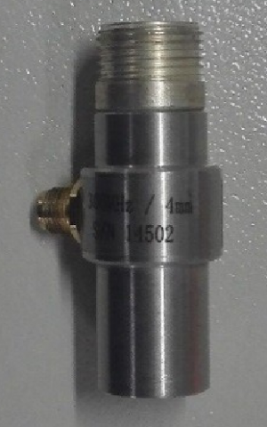
Take the high-frequency ultrasonic transducer 14502 used herein as an example, the center frequency f=300MHz, the aperture a0=1.5mm, the focal length F=4mm; λ0 is the wavelength of the acoustic wave in the couplant. It is assumed that the sound velocity in the water c=1480m/s, according to Formulas (1), (2), (3), theoretical resolution of the transducer for detection can be calculated:
w1=6.71μm; w2=9.49μm; BD=13.42μm
2.2 Lateral dimension measurement resolution
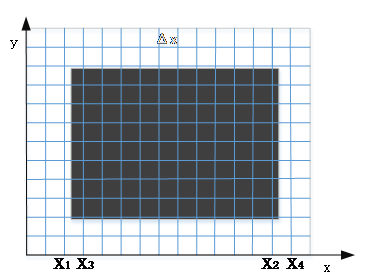
The measurement of the lateral dimension is meant to measure the least change in the minimum lateral dimension, as shown in Figure 2, it is the relationship of the scan image with the DUT.
(a) (b)
Figure 2. Relationship between DUT and scan image
As shown in Figure 2 (a), in an ideal state, the boundary of the DUT is exactly at the boundary of scan image pixels, and now the measured size L is:
$L=(X_2-X_1)\cdot l$ (4)
where, l is the calibration value per unit pixel.
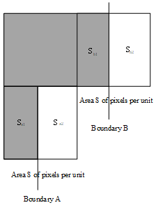
In Figure 2(b), the boundary of the DUT is not at the boundary of the pixels of the scan image, but may be any value between X1 and X3. At this time, it is required to determine whether the pixel passed by the boundary is zero (as shown in the left side of Figure 5) or has a value (as shown in the right side of Figure 5). The pixel value of microscopic image is available by the peak conversion of reflected echo in the gate. When the maximum peak of the echo in the gate is less than the gate threshold, the pixel value is zero. When the maximum peak of the echo in the gate is greater than the gate threshold, it is likely to obtain a pixel value rather than zero. And because the size of echo peak is subjected to the area of the pixels of boundary the DUT occupies, that is, the larger the area, the greater the peak of the reflected echo can be obtained. Assume the area of boundary pixels when the reflected echo peak is equal to the gate threshold is SK. As shown in Figure 5, it is supposed the area occupied by the DUT at the boundary pixel is S1. When S1 < SK, the boundary of the DUT locates in the right boundary of the pixel; when S1 > SK, it is at the left boundary of the pixel. That is, as shown in Figure 6, in order to distinguish the boundaries A from B, it should be ture that the image boundary formed by boundary A is located on the left side of the boundary pixels or on the right side of the boundary B, that is,
Sa1<SK (5)
or
Sb1>SK (6)
Then Sa2 + Sb1 > S, approximated as Xb - Xa > x (Xa, Xb are the actual coordinates of the boundaries A and B, respectively; x is the unit pixel value). It is bound to differentiate the boundaries A from B.
Figure 3. Analysis map whem boundary fall within pixels
Figure 4. Pixel map of boundaries A, B
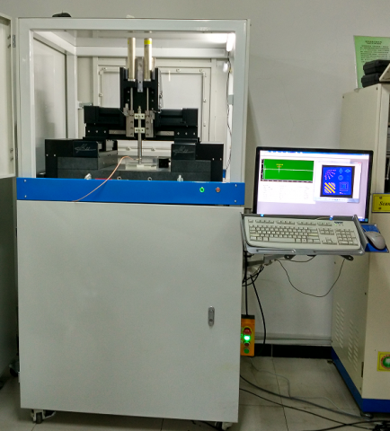
Ultrasound microscopy system with high frequency includes the precision motion controller and the high frequency ultrasound exciter and receiver system. The former consists of the motion control card and X, Y, Z scan racks. As the principle is concerned, the motion control card controls the X, Y and Z scan axes that drive the transducer to fulfill the scan process, whilst timely recording and feeding back the coordinate information about each axle. During scaning process, a synchronous position trigger signal is provided to excite the signal generator and the data acquisition card. The high-frequency ultrasonic exciter and receiver system transmits, receives and acquires high-frequency ultrasonic signals. It consists of high-frequency focused ultrasonic transducers, signal generators, high-frequency data acquisition card, amplifier and so on. Here we use a high frequency focused transducer with center frequency of 300 MHz, prodvied by the Germany PVA. The system diagram and transducer are shown in Figure 5.
Figure 5. High-frequency scanning acoustic microscopy measurement system and high-frequency ultrasonic transducer
4.1 Defect sample measurement test
In this test, a defective silicon wafer, 10mm×10mm×0.5mm (H), self-designed by the laboratory, is sampled. From the surface of the silicon wafer, it is machined into a variety of shapes with a depth of 200μm and a width of 10μm ~ 400μm by laser etching process. Then, machined silicon wafer is bonded with a silicon wafer with a same size and thickness to form an internally sealed structure, see Figure 6 for its internal design.
Figure 6. Internal structure design of defective silicon wafer
Table 1. Scan range, accuracy, and speed settings for scan and index axes
|
Parameter |
Length (mm) |
Speed (mm/s) |
Accuracy (mm) |
Accrucy (mm) |
Accrucy (mm) |
Accrucy (mm) |
|
Scan axis |
12 |
50 |
0.1 |
0.05 |
0.01 |
0.005 |
|
Index axis |
12 |
5 |
0.1 |
0.05 |
0.01 |
0.005 |
(a) Scan accuracy 0.1mm (b) Scan accuracy 0.05mm
(c) Scan accuracy 0.01mm (d) Scan accuracy 0.005mm
(e) Patially enlarge map
Figure 7. Scan image of silican wafer
The resulting C-scan image is shown in Figure 7. It is obvious that the internal defects available when the scan pitch is 0.1mm are relatively fuzzy, but as the scan accuracy increases, the defects seem clearer and clearer. When the scan accuracy falls within 0.01~0.005, the image resolution is identical. This result shows that the C-scan image resolution is subject to the scan pitch, that is, the lower the scan pitch, the higher the resolution. However, the image resolution does not change when the scan pitch reaches a certain value. When the scan pitch is 0.005mm, the lines of different lengths from 25μm to 500μm can be clearly seen, including square, circular and diamond line rings with a minimum width of 10μm, and round holes with different diameters. For the round hole in the lower right corner, it is known from the design drawing that there are 25 round holes with diameter increasing from 10μm to 60μm. From the scan image, there are total 22 round holes whose diameters are in descending order. The high-frequency focus transducer 14502 provided by PVA company can recognize a circular hole with a minimum diameter of 16μm. Compared to the three resolution criteria, the actual resolution is closer to that of the beam diameter method.
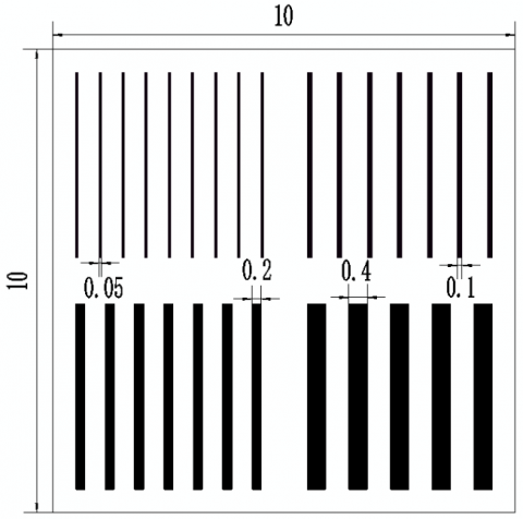
4.2 Sample width measurement test
In this test, a square micron-sized silicon wafer, 10mm×10mm×0.5mm (H), of micron order, self-designed, is used, see Figure 8 for finish size designed internally. After laser etching process, the test block is bonded together with the same size of silicon wafer to form a sample that can be used to test the lateral dimension measurement from the system on the internal microsize. The resulting C-scan image is shown in Figure 9.
Figure 8. Silicon wafer sample for width test
Figure 9. Internal size scan image of SW sample for width test
With similar scanning conditions, 10 scans are performed, and the lines with four widths in the image are measured for 10 times, see Table 2 for the measurement results. As show in Table 2, the error of lines at the width of 50 μm is 5.05 %, and the measurement error decreases with the increase in size; the measurement error of lines at 400 μm is 0.64 %.
Table 2. Dimension measurements of silicon wafers
|
Design value (μm) |
Mean of 10 measurements (μm) |
Offset (μm) |
Error (μm) |
|
50 |
52.525 |
2.525 |
5.05 % |
|
100 |
103.046 |
3.046 |
3.05 % |
|
200 |
204.143 |
4.143 |
2.072 % |
|
400 |
402.553 |
2.553 |
0.64 % |
Based on the principle of ultrasonic microscopic C-scan image measurement, the lateral resolution of the high-frequency scanning acoustic microscopy system is analyzed. There are three theoretical models for C-scan imaging resolution, i.e. the Rayleigh criterion, the Sparrow criterion and the beam diameter, based on which, the resolution of 300MHz high-frequency focused transducer can be calculated with the lateral measurement resolution analyzed. Lastly, the C-scan imaging tests were conducted on the self-designed silicon wafer samples for width and defects by the high-frequency scanning acoustic microscopy system. Test results show that the more precise the scan pitch is, the higher the resolution, however, when the scan pitch is traceable to a specified value, the resolution is less subject to it. At this time, the lateral resolution is closer to that by the beam diameter. However, thanks to the factors such as practical design process of the transducer, the lateral resolution available acturally is lower than the theoretical value.
Supported by the Key National Natural Science Foundation of China (Grant No. 51335001, U1737203).
[1] Brand S, Lapadatu A, Djuric T. (2014). Scanning acoustic gigahertz microscopy for metrology applications in three-dimensional integration technologies. Journal of Micro/Nanolithography MEMS, and MOEMS 13(1): 1-9. https://doi.org/10.1117/1.JMM.13.1.011207
[2] Brand S, Vogg G, Petzold M. (2018). Defect analysis using scanning acoustic microscopy for bonded microelectronic components with extended resolution and defect sensitivity. Microsystem Technologies 24: 779-792. https://doi.org/10.1007/s00542-017-3521-7
[3] Jasiuniene E, Zukauskas E, Dragatogiannis DA, Koumoulos EP, Charitidis CA. (2017). Investigation of dissimilar metal joints with nanoparticle fillers. NDT & E International 92: 122-129. https://doi.org/10.1016/j.ndteint.2017.08.005
[4] Brand S, Czurratis P, Hoffrogge P. (2011). Extending acoustic microscopy for comprehensive failure analysis applications. Journal of Materials Science Materials in Electronics 22(10): 1580-1593. https://doi.org/10.1007/s10854-011-0487-6
[5] Raum K, Ozguler A, Morris S, O’Brien Jr WD. (1998). Channel defect detection in food packageg using integrated backscatter ultrasound imaging. IEEE Transactions on Ultrasonics Ferroelectrics and Frequency Control 45(1): 30-40. https://doi.org/10.1109/58.646905
[6] Atalar A. (1985). Penetration depth of the scanning acoustic microscope. IEEE Transactions on Sonics and Ultrasonics 32(2): 164-167. https://doi.org/10.1109/T-SU.1985.31583
[7] Yin JF, Bai Q, Zhang B. (2018). Methods for detection of subsurface damage: A Review. Chinese Journal of Mechanical Engineering 31(3): 31-41. https://doi.org/10.1186/s10033-018-0229-2
[8] Lu XN, Liu F, He ZZ. (2018). Defect inspection of flip chip package using SAM technology and fuzzy C-means algorithm. Chinese Science: Technical Science: 61(9): 1426-1430. https://doi.org/10.1007/s11431-017-9185-6
[9] Liu F, Su L, Fan M, Yin J, He Z, Lu X. (2017). Using scanning acoustic microscopy and LM-BP algorithm for defect inspection of micro solder bumps. Microelectronics Reliability 79: 166-174. https://doi.org/10.1016/j.microrel.2017.10.029
[10] Su L, Zha Z, Lu X, Shi T, Liao G. (2013). Using bp network for ultrasonic inspection of flip chip solder joints. Mechanical Systems and Signal Processing 34(1-2): 183-190. https://doi.org/10.1016/j.ymssp.2012.08.005
[11] Lee CS, Zhang GM, Harvey DM, Qi A. Characterization of micro-crack propagation through analysis of edge effect in acoustic microimaging of microelectronic packages. NDT & E International 79: 1-6. http://dx.doi.org/10.1016/j.ndteint.2015.11.007
[12] Zhang Y, Shi T, Su L, Wang X, Hong Y, Chen K, Liao G. (2016). Sparse reconstruction for micro defect detection in acoustic micro imaging. Sensors 16: 1773. https://doi.org/10.3390/s16101773
[13] Fei D, Rebinsky DA, Zinin P, Koehler B. (2004). Imaging defects in thin DLC coatings using high frequency scanning acoustic microscopy. AIP Conference Proceedings 700(1): 976. https://doi.org/10.1063/1.1711724
[14] Maeva E, Severin F, Miyasaka C. (2009): Acoustic imaging of thick biological tissue. IEEE Transactions on Ultrasonics, Ferroelectrics, and Frequency Control 56(7): 1352-1358. https://doi.org/10.1109/TUFFC.2009.1191
[15] Rohrbach D, Jakob A, Lloyd HO, Tretbar SH, Silverman RH, Mamou J. (2017). A novel quantitative 500-MHZ acoustic microscopy system for ophthalmologic tissues. IEEE Transactions on Biomedical Engineering 64(3): 715-724. https://doi.org/10.1109/TBME.2016.2573682
[16] Jipson V, Quate CF. (1978). Acoustic microscopy at optical wavelengths. Applied Physics Letters 32(12): 789-791. https://doi.org/10.1063/1.89931
[17] Heiserman J Rugar D, Quate CF. (1980). Cryogenic acoustic microscopy. Journal of the Acoustical Society of America 65(5): 1629-1637. https://doi.org/10.1016/0041-624X(72)90224-7
[18] Hadimioglu B, Quate CF. (1983). Water acoustic microscopy at suboptical wavelengths. Applied Physics Letters 43(11): 1006-1007. https://doi.org/10.1063/1.94223
[19] Foster JS, Rugar D. (1983). High resolution acoustic microscopy in superfluid helium. Applied Physics Letters 42(10): 869-871. https://doi.org/10.1016/0378-4363(84)90164-5
[20] Briggs A, Briggs GAD, Kolosov O. (2010). Acoustic microscopy. New York: Oxford University Press.
[21] Canumalla S. (1999). Resolution of broadband transducers in acoustic microscopy of encapsulated ics: transducer selection. IEEE Transactions on Components and Packaging Technology 22(4): 582-592. https://doi.org/10.1109/6144.814975
[22] Olympus. (2007). Ultrasonic transducers technical notes.