Hassen Kaddour* | Abderrahmane Dib
© 2021 IIETA. This article is published by IIETA and is licensed under the CC BY 4.0 license (http://creativecommons.org/licenses/by/4.0/).
OPEN ACCESS
This paper presents a recent technique for photovoltaic grid connected systems based on the use of the (DPC-SVM) to select the optimal switching states to apply to the inverter, where the extended reactive power is used instead of reactive power. This technique allows achieving an optimal control of the inverter which manifests in controlling the converters using an MPPT algorithm instead of controlling each part separately. This yields to a reduced global control system on a large scale. In this context, we suggest a DC-DC boost converter circuit to ensure better behavior of the system. The FMV technique is used to inject specific harmonics in order to eliminate or minimize the undesired harmonics. The SVM model has also been developed for optimal control of the inverter to prove the high performance of the proposed method. All the results are analyzed theoretically. The simulation has shown that this strategy gives satisfactory performances, improvement of the power factor and a reduction of the THD by 37%.
Direct Powers, Control (DPC), Space Vector, Modulation (SVM), Total Harmonics, Distortion (THD, Multi-variable Filter (FMV)
Energy production has been always a major challenge due to the growing energy needs as populations and industrial communities increase. As a result, developed countries will need more and more energy to implement their development. There are several types of renewable energy sources, such as the photovoltaic energy. Although photovoltaic energy has been known for years as a source of electric power from a few watts to a few megawatts, it is an interesting alternative to traditional energy sources due to its advantages [1].
In recent years, several researchers are working to develop photovoltaic system control techniques to maximize the production of electrical energy from the solar power [2]. Several suggestions have been proposed by researchers for developing grid connected systems, including DC-DC converters. Many topologies of DC-DC converters have been designed for the purpose of improving the efficiency [3], such as the resonant type transformers that use zero current conversion or zero voltage switching and the DC-AC conversion system which uses the CLC resonant type full-bridge DC-DC converter [4] and new DC-DC non-isolated high gain converter called Double Zeta Quadratic Converter [5] and combination of two boost stages namely Quadratic Boost Zeta and Isolated Zeta forming Integrated Quadratic Boost Converter with high static voltage gain [6].
However, in this type of transformers, the volume of the circuit increases. Another DC-DC adapter topology has been used to improve production efficiency [1].
In addition to that, various methods of controlling power have been taken care of under unbalanced network conditions. In the paper [7], the author proposes Direct Powers Control with Space Vector Modulation (DPC-SVM), this is to eliminate power fluctuations and obtain a constant switching frequency. One of the advantages of DPC-SVM is that it eliminates the switch table and uses SVM block so that the switching frequency becomes constant [8]. This ensures a good energy transfer between the PV and the grid; it also has lower sampling frequency than a conventional DPC which help overcome the problem of energy fluctuations. The vector modulation technique is therefore used to achieve a fixed switching frequency and less power pulsations [9, 10].
In the study [11] DPC-SVM is used to obtain constant active power and sinusoidal network currents using the extended energy theory [12]. Whereas Ouchen et al. [13] proposed to improve the replacement of PI controllers with second order sliding mode controllers (ST-SMC) in active and reactive power control loops. Benbouhenni [14] proposed controller in the neural sliding mode based on neural pulse width modulation (NPWM), whereas in the paper [15] the author proposes DPC based on the neural super-twisting sliding mode (NSTSM). Heydari et al. [16] presented DPC based on the fuzzy logic and genetic algorithm (GA). According to the research [17], the performance and strength of conventional DPC and the NDPC-NPWM method are compared.
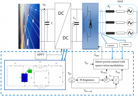
In this paper we study a PV system connected to network using an optimized DC-DC boost converter with injected harmonic in the command Direct Powers Control using Space Vector Modulation (DPC-SVM). Conventional DPC-SVM has also been improved so that actual power can accurately track its reference. We will also talk about the role of SVM in improving power fluctuations and obtaining a stable switching frequency.
In the first stage, we start by explaining the concept of the DC-DC converter used and how it operates; in the second stage: We explain the process of injecting harmonics using the technique FMV to eliminate or minimize the undesired harmonics.
In the first stage: the converter circuit is working as a lever for voltage, its rate of increasing is much greater than the conventional converter. The circuit has two identical capacitors that are charged in parallel and are automatically unloaded by the on-off (1-0) transition of the main switching device. The circuit is similar to the conventional circuit but differs in connecting the capacitors c1 and c2
In case S1=0, the two capacitors are charged at the same time.
In case S1=1, the capacitors are discharged at the same time to the output circuit when connected in series by S1.
This proposed converter is capable for giving voltage in the output larger, this converter is better than conventional boost converter.
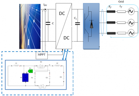
The studied system is shown in Figure 1. The global system is made up of three main blocks: The first is a PV system that provides power for the circuit. Using the proposed DC-DC boost converter that is controlled by a P&O MPPT controller. The second consists of a DPC-SVM for the inverter which has two main roles: the first one is combining between the network and the PV system through filter and the second is to compensate the harmonics and reactive power, the third is the three-phase grid.
Figure 1. Schematic circuit diagram of a three-phase grid
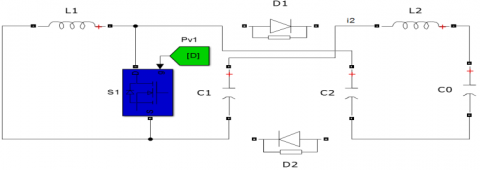
Figure 2. Model of the high gain DC-DC boost converter circuit [1]
The proposed DC-DC converter can provide higher output voltage than the conventional boost [18], thanks to the two capacitors (c1,c2) attached in parallel as shown in Figure 2.
2.1 Design of the circuit
In the circuit studied in Figure 2, we set (t = 0) at the beginning of each running mode.
By analyzing the circuit, we find two states: switch on, corresponds to state “1” while the state is “0” when, the switch off.
In the first case as shown in Figure 3 the value of the current I1 is given by Eq. (1):
Suppose initial value of i1(0)=I1min
$i_{1}=I_{1 \min }+\frac{V_{P V}}{L_{1}} t$ (1)
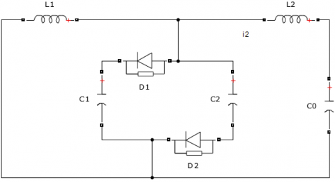
The capacitors C1 and C2 are connected in series. In this time interval the capacitor C0 is charged from the resultant capacitor voltage and the resultant capacitor voltage of VC1=2VC charges the output capacitor C0. In addition, the capacitor C0 charges from the resultant capacitor voltage and the following equations explain how the current i2 flows through the inductor L2.
Figure 3. Circuit in case "1" [1]
$L_{2} \frac{d i_{2}}{d t}+\frac{2}{C} \int \cdot i_{2} d t=-c_{0} i_{0}$ (2)
Since C1 is equal to C2 we put C in the upcoming equations. We get the equation of i2 as follows:
$i_{2}(t)=X+Y$ (3)
$\left\{\begin{array}{c}X=I_{2 \min } \cos \sqrt{\frac{2}{C L_{2}}} t \\ Y=\sqrt{\frac{C}{2 L_{2}}}\left(2 V_{C \max }-V_{0}\right) \sin \sqrt{\frac{2}{C L_{2}}} t\end{array}\right.$
where, $\mathrm{i}_{2}(0)=\mathrm{I}_{2 \mathrm{~min}}$
$V_{C}(0)=V_{C 1}(0)=V_{C 2}(0)=-V_{C \max }$ (4)
Integrating Eq. (3) will give:
$V_{C}=A+B+C$ (5)
$\left\{\begin{array}{c}A=\sqrt{\frac{L_{2}}{2 C}} I_{2 \min } \sin \sqrt{\frac{2}{C L_{2}}} t \\ B=\frac{1}{2}\left(2 V_{C \max }-V_{0}\right) \cos \sqrt{\frac{2}{C L_{2}}} t \\ C=\frac{V_{0}}{2}\end{array}\right.$
The circuit analysis during mode 2 (switch “0” interval) as shown in Figure 4 gives:
$i_{1}(t)=I_{1 \max }+\frac{V_{p n}-V_{C}}{L_{1}} t$ (6)
Suppose $\mathrm{i}_{1} \cdot(0)=\cdot \mathrm{I}_{1 \mathrm{max}}$:
The equation in the output is as follows:
$L_{2} \frac{d i_{2}}{d t}-\frac{1}{C} \int i_{C} d t=-V_{0}$ (7)
Figure 4. Circuit in case "0" [1]
$2 i_{C}=i_{1}-i_{2}$ (8)
We put $\mathrm{i}_{1}=$ constant and it’s given:
$i_{1}(t)=I_{1} \operatorname{cons}(t)$
$v_{C}=V_{C m i n}$ (9)
$i_{2}=I_{2 \max }$
By using Eqns. (7), (8) and (9), we have:
$i_{2}(t)=\alpha+\beta$ (10)
$\left\{\begin{array}{c}\alpha=I_{1}\left\{1-\cos \sqrt{\frac{1}{2 L_{2} C}} t\right\}+I_{2 \max } \cos \sqrt{\frac{1}{2 L_{2} C}} t \\ \beta=\sqrt{\frac{2 C}{L_{2}}}\left(V_{C \min }-V_{0}\right) \sin \sqrt{\frac{1}{2 L_{2} C}} t\end{array}\right.$
$v_{c}(t)=k+h+g$ (11)
$\left\{\begin{array}{c}k=\frac{1}{2} \sqrt{\frac{2 L_{2}}{C}}\left(I_{1}-I_{2 \max }\right) \sin \sqrt{\frac{1}{2 L_{2} C}} t \\ h=\left(V_{C m i n}-V_{0}\right) \cos \sqrt{\frac{1}{2 L_{2} C}} t \\ g=V_{0}\end{array}\right.$
To compare the conventional converter with the proposed converter, we compare their output signal amplification and the output voltage ripple along with the input current ripple.
2.1.1 Input current ripple
We put the input current ripple for the conventional boost converter and the proposed converter equal in value. We put the duty ratio $\alpha_{\mathrm{N}}$ and current ripple $\cdot \Delta \mathrm{I}_{1 \mathrm{~N}}$ for the proposed converter. $\alpha_{\mathrm{C}}$ and $\cdot \Delta \mathrm{I}_{1 \mathrm{C}}$. for the conventional boost converter. Using Eq. (1) give the following:
$\frac{\Delta I_{N}}{\Delta I_{C}}=\frac{\alpha_{N}}{\alpha_{C}}$ (12)
When $\alpha_{\mathrm{N}}$ and $\alpha_{\mathrm{C}}$ are related, the same voltage is produced for the proposed and the conventional boost converter as follows:
$\alpha_{N}=\frac{\alpha_{C}}{2-\alpha_{C}}$ (13)
We put Eq. (13) in Eq. (12) we get:
$\frac{\Delta I_{N}}{\Delta I_{C}}=\frac{1}{2-\alpha_{G}}<1$ (14)
Therefore, the input current ripple is smaller than the conventional current transformer knowing that the same initial characteristics were provided for each circuit, which is one of the advantages of the new circuit.
2.2 Output voltage ripple
The load current $I_{0}$, in the conventional boost circuit is given by capacitor $\cdot \mathrm{C}_{0}$ during the " $1^{\prime \prime}$. interval. We put $\mathrm{I}_{0}$. constant, in this case the voltage ripple $\Delta V_{\text {oc }}$ is given by:
$\Delta V_{0 C}=\frac{I_{0}}{C_{0}} \alpha_{C} T=\frac{1}{C_{0}} \frac{V_{0}}{R_{0}} \alpha_{C} T$ (15)
The output current approximated in each mode is illustrated in Figure 5 and the output voltage ripple is given by:
$\Delta V_{0 C}=x+y=\frac{1}{8 C_{0}} \Delta I_{2} T$ (16)
$\left\{\begin{array}{c}x=\frac{1}{C_{0}} \int_{0}^{\alpha T / 2} \frac{\Delta I_{2}}{\alpha T} t d t \\ y=\frac{1}{C_{0}} \int_{0}^{(1-\alpha) T / 2}\left[\frac{\Delta I_{2}}{2}-\frac{\Delta I_{2}}{(1-\alpha) T} t\right] d t\end{array}\right.$
We put $V_{\mathrm{Cmax}}=\cdot V_{0}$ to get the following formula:
$\Delta V_{0 N}=\frac{1}{8 C_{0}} \frac{V_{0}}{L_{2}} \alpha_{N} T^{2}$ (17)
To compare the voltage ripple in the conventional converter with the proposed converter, we compare Eq. (17) and Eq. (15) on the condition of having the same output voltage.
Figure 5. Diagram of the new circuit voltage [1]
$\frac{\Delta V_{0 N}}{\Delta V_{0 C}}=\frac{1}{8} \frac{R}{L_{2}\left(2-\alpha_{C}\right)} T$ (18)
Using the Eq. (18), the new voltage ripple can be evaluated. Discussion has shown that the proposed circuit provides higher output voltage with better stability.
The DPC-SVM with constant switching frequency uses closed-loop power control [7]. As shown in Figure 6, the output signals are transformed to the fixed frame to generate the switching signals by the space-vector modulator (SVM) [18].
Figure 6. DPC with space vector modulation (DPC-SVM)
We need the grid and converter voltages and their delayed values to derive the power compensation to add to the power references. Constant DC-link voltage and sine grid currents are achieved simultaneously without affecting the reactive power and average active power value at the network side.
One of the positives of this proposed method is to nullifying the oscillations active and reactive power.
The complex power is defined as:
$S=\frac{3}{2}\left(e i^{*}\right)$ (19)
The active and reactive power of the complex power:
$p=\frac{3}{2} \operatorname{Re}\left(e i^{*}\right)$ (20)
$q=\frac{3}{2} \operatorname{Im}\left(e i^{*}\right)$ (21)
In the paper [19], complex power is defined as:
$q^{e x t}=\frac{3}{2} \operatorname{Im}\left(e^{\prime} i^{*}\right)$ (22)
The proposed method proved great in eliminating oscillations compared to the conventional method, using qext) with active power. As a result, the cancellation of the active power ripple will naturally lead to the elimination of reactive power ripple while obtaining sinusoidal current. The grid voltage and current consist of positive and negative sequence components.
$e=e^{+}+e^{-}=E_{d a}^{+} e^{j w t}+E_{d q}^{-} e^{-j w t}$ (23)
é $=j E_{d q}^{+} e^{j w t}+E_{d q}^{-} e^{-j w t}$ (24)
Derivative “active power” and “extended reactive power”.
$\frac{d p}{d t}=\frac{3}{2} \operatorname{Re}\left(\frac{d e^{\prime}}{d t} i^{*}+e^{\prime} \frac{d i^{*}}{d t}\right)$ (25)
$\frac{d q^{e x t}}{d t}=\frac{3}{2} \operatorname{Re}\left(\frac{d e^{\prime}}{d t} i^{*}+\dot{e} \frac{d i^{*}}{d t}\right)$ (26)
Derivative (19) and (20) are as follows:
$\frac{d e}{d t}=j \omega e^{+}-j \omega e^{-}=\omega e^{\prime}$ (27)
$\frac{d e}{d t}=\omega e^{+}-\omega e^{-}=\omega e$ (28)
$\frac{d i}{d t}=\frac{1}{L}(e-v-r i)$ (29)
Compensation (23) and (25) into (21) and (22) respectively:
$\frac{d p}{d t}=\frac{1.5}{L}\left[|e|^{2}-\operatorname{Re}\left(e v^{*}\right)\right]-\frac{R}{L} p-\omega q^{e x t}$ (30)
$\frac{d p^{e x t}}{d t}=\frac{1.5}{I} \operatorname{Re}\left[\left(e^{*}-v^{*}\right) e^{\prime}\right]-\frac{R}{L} q^{e x t}-\omega p$ (31)
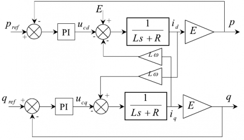
The errors of the active and reactive powers are applied to the respective PI regulators. The output in the (d-q) vectorial space system is the voltages ($\mathrm{u}_{\mathrm{cd}}, \mathrm{u}_{\mathrm{cq}}$), as shown in Figure 7 [20, 21].
The coefficients of the power regulators PI can be calculated by a simplified model of the rectifier in (d. q) frame, the model in the repository d-q is given by Eq. (32):
$\left\{\begin{array}{l}e_{d}=R i_{d}+L \frac{d i_{d}}{d t}-w L i_{q}+u_{e d} \\ e_{q}=R i_{q}+L \frac{d i_{q}}{d t}-w L i_{d}+u_{e q}\end{array}\right.$ (32)
From which the Eq. (33) becomes:
$\left\{\begin{array}{l}E=R i_{d}+L \frac{d i_{d}}{d t}-w L i_{q}+u_{e d} \\ 0=R i_{q}+L \frac{d i_{q}}{d t}-w L i_{d}+u_{e q}\end{array}\right.$ (33)
Figure 7. Block diagram of the loops of p and q with two correctors PI
With the introduction of the power regulator PI block, the following diagram is obtained (Figure 8) [20]:
If we assume that the reactive power is zero that is iq=0, the loop of regulation of the reactive power can be eliminated as shown in Figure 8.
Figure 8. Active power regulator [18]
The line voltage is considered as a constant and must be compensated by the integral part of the corrector PI.
The closed loop transfer function is given by:
$G(s)=\frac{E\left(k_{p} s+k_{i}\right)}{L s^{2}+\left(E k_{p}+R\right) s+E k_{i}}$ (34)
The transfer function of a second-order in closed-loop system is given by:
$F(s)=\frac{1}{\left(s^{2}+2 \varepsilon \omega_{n} s+\omega_{n}^{2}\right)}$ (35)
By analogy between an expression (34) and (35) finds:
$\left\{\begin{array}{c}k_{p}=\frac{2 \cdot L \cdot \varepsilon \omega_{n}-R}{E} \\ k_{i}=\frac{L \cdot \omega_{n}^{2}}{E}\end{array}\right.$ (36)
It should be noted that the Eq. (36) is valid for the two correctors.
To verify the performance and the feasibility of the DPC-SVM with the proposed DC-DC converter applied on the PV system connected with shunt active power filter, a digital simulation has been carried out using MATLAB/SIMULINK software that compare the performance of the conventional [22] and the proposed converter under the same command of the DC-DC converter (P&O) and parameters (Table 1).
Table 1. System parameters
|
Parameter |
Value |
|
RL resistance |
0.3 Ω |
|
LL inductance |
8 mH |
|
C capacitor |
0.0011 F |
|
Ts Sampling Time |
50 $\mu \mathrm{s}$ |
|
f frequency |
50 HZ |
|
fc Switching frequency (DPCSVM) |
15KHZ |
By comparing both the results of the proposed converter and the conventional converter [23], the obtained simulation results show the efficiency and performance of the proposed DC- DC converter.
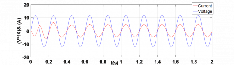
Figure 9-A shows the voltage and Line current waveforms, we observe that the current line has has less oscillation.
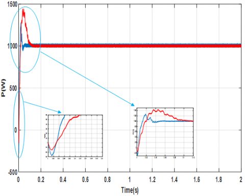
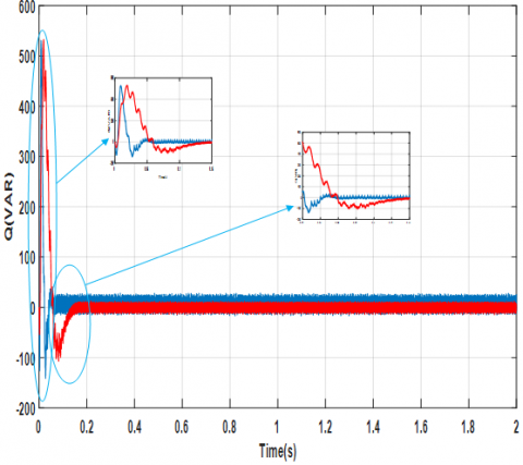
Figure 9-B and Figure 9-C show the instantaneous active and reactive power. It can be seen that the active and reactive power have a good time response and less ripple with the proposed DC-DC converter without oscillations. When comparing the active power between the conventional and the proposed method we find that the conventional active power has a response in t = 0,15s, while the response time of the new active power in t = 0,05s, this proves the advantage of the proposed method.
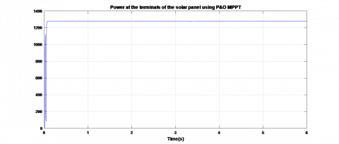
Figure 9-D and Figure 10-D show the power solar panel using P&O MPPT. We put the same values to compare the performance of the proposed and the conventional converter
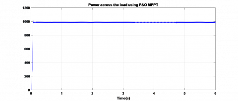
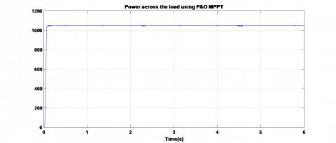
Figure 9-E and Figure 10-E show the power across the load using P&O MPPT. We observe that the proposed DC-DC converter amplifies the output signal larger than the output signal of the conventional converter and a rapid time response and low ripple.
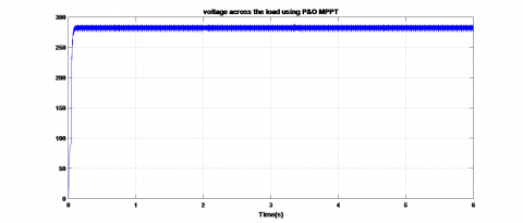
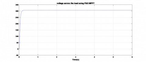
In Figure 9-F and Figure 10-F we observe that the voltage across the load is larger in the proposed DC-DC converter and a smaller time response and low ripple.
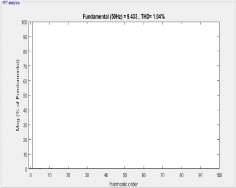
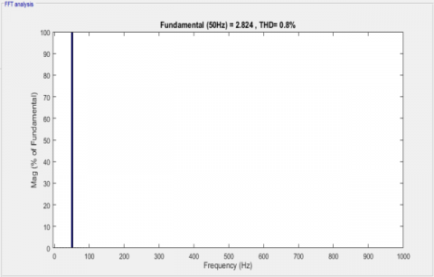
Figure 9-G and Figure 10-G show the voltage across the solar panel using P&O MPPT. We observe that the output voltage of the proposed DC-DC converter is larger than that of the conventional converter with faster response and less ripple. Figure 9-L and Figure 10-L shows the Harmonic spectrum of the line current when we obtained the value of THD is 1.04% with classical DC-DC and 0.87% with proposed DC-DC.
The simulation results are very satisfying and show that the adopted technique improves the power factor and reduces the Total Harmonics Distortion to about 37%.
A. Voltage and line current
B. Instantaneous active power conventional (red) and new (blue)
C. Instantaneous reactive power conventional (red) and new (blue) Classical DC-DC converter
D. Power at the terminals of the solar panel using P&O MPPT
E. Power across the load using P&O MPPT
F. Voltage across the load using P&O MPPT
G. Voltage across the solar panel (v)
L. Harmonic spectrum of the line current (THD = 1.04%)
Figure 9. Results of simulations of the DPC–SVM with Classical DC–DC converter
D. Power at the terminals of the solar panel using P&O MPPT
E. Power across the load using P&O MPPT
F. Voltage across the load using P&O MPPT
G. Voltage across the solar panel (v)
L. Harmonic spectrum of the line current (THD = 0.8%)
Figure 10. Results of simulations of the DPC – SVM with proposed DC-DC converter
In this paper, we used extended reactive power instead of reactive power usually used in conventional DPC-SVM. so that actual power can accurately track its reference. Also, we controlled the converters using MPPT algorithm at the same time, and not controlling each one separately. Moreover, we described the basics, circuit parameter and design of a proposed DC-DC boost converter circuit that gives a larger step-up ratio.
The simulation results confirmed that the DPC-SVM with the DC-DC converter could decreases the losses; raise the voltage at the output with a better stability and much greater voltage than the conventional boost converter with a better input and output ripple characteristics.
The DPC-SVM has shown high efficiency and stability in the system. Also, the THD and active and reactive power were improved using extended reactive power as the results showed. Where we noticed improvement in active and reactive power’s response where it stabilized on a value in lesser time. Also, the stability was improved where there was not much ripples comparing to the conventional DPC-SVM as demonstrated in (Figure 9-B, Figure 9-C). Also we recorded a decreasing in the value of THD (0.8%) using the proposed DPC-SVM technique (Figure 10-L)).
Therefore, we conclude that our system with proposed DC-DC converter have a good performance such as stability, robustness and smaller ripples comparing to the classical DC-DC converter and also recorded a decrease in harmonic ratio.
|
MPPT |
Maximum Power Point Tracking |
|
VPV |
PV array voltage (V) |
|
IPV |
PV array current (A) |
|
Sa,Sb,Sc |
Switching state |
|
Kp |
Proportional gain |
|
Ki |
Integral gain |
|
Pref |
Reference active power |
|
Qref |
Reference reactive power |
|
Vdc,Vdcref |
Actual and reference Vdc |
|
$\omega_{n}$ |
Natural frequency |
|
PI |
Proportional-integral |
|
DPC |
Direct power control |
|
SVM |
Space vector modulation |
|
THD |
Total harmonic distortion |
|
$\alpha_{\mathrm{N}}$ |
Duty ratio |
|
$\mathrm{C}_{1}$ et $\cdot \mathrm{C}_{2}$ |
Capacitor |
|
S1 |
Switch |
|
L1 et L2 |
Inductance |
|
Rf et Lf |
Grid filter resistance and inductance |
|
$\Delta \mathrm{I}_{1 \mathrm{N}}$ |
Current ripple |
|
$\mathrm{V}_{\mathrm{C} 1}$ et $\cdot \mathrm{V}_{\mathrm{C} 2}$ |
Capacitor Voltage |
|
C0 |
Output Capacitor |
|
I0 |
Output Current |
|
V0 |
Output Voltage |
|
Ts |
Control period |
[1] Nomura, H., Fujiwara, K., Kochi, M.Y. (2006). A new DC-DC converter circuit with larger step-up/down ratio. 2006 37th IEEE Power Electronics Specialists Conference, Jeju, Korea (South), pp. 1-7. https://doi.org/10.1109/pesc.2006.1712228
[2] Ouchen, S., Abdeddaim, S., Betka, A., Menadi, A. (2016). Experimental validation of sliding mode-predictive direct power control of a grid connected photovoltaic system, feeding a nonlinear load. Solar Energy. 137: 328-336. https://doi.org/10.1016/j.solener.2016.08.031
[3] Hirachi, K., Yamanaka, M., Kajiyama, K., Isokane, S. (2002). Circuit configuration of bidirectional DC/DC converter specific for small scale load leveling system. Proceedings of the Power Conversion Conference-Osaka 2002 (Cat. No.02TH8579), Osaka, Japan, pp. 603-609. https://doi.org/10.1109/PCC.2002.997586
[4] Huynh, D.M., Ito, Y., Aso, S., Kato, K., Teraoka, K. (2018). New concept of the DC-DC converter circuit applied for the small capacity uninterruptible power supply. International Power Electronics Conference (IPEC-Niigata 2018 -ECCE Asia), Niigata, Japan, pp. 3086-3091. https://doi.org/10.23919/IPEC.2018.8507821
[5] Sa, F.L., Agnol, C.D., Raphael, W., Caballero, D.R., Mussa, S.A. (2020). A new DC-DC Double Zeta Quadratic Converter. IEEE International Conference on Industrial Technology (ICIT), Buenos Aires, Argentina, pp. 426-431. https://doi.org/10.1109/ICIT45562.2020.9067314
[6] Meghna, Chauhan, Y.K. (2018). PV water pumping using integrated quadratic boost zeta converter. International Conference on Power Energy Environment and Intelligent Control (PEEIC), Greater Noida, India, pp. 120-125. https://doi.org/10.1109/PEEIC.2018.8665640
[7] Malinowski, M., Jasinski, M., Kazmierkowski, M.P. (2004). Simple direct power control of three-phase PWM rectifier using space-vector modulation (DPC-SVM). IEEE Transactions on Industrial Electronics, 51(2): 447-454. https://doi.org/10.1109/TIE.2004.825278
[8] Zhang, Y.C., Liu, J., Yang, H.T., Gao, J.H. (2018). Direct power control of pulsewidth modulated rectifiers without DC voltage oscillations under unbalanced grid conditions. IEEE Transactions on Industrial Electronics, 65(10): 7900-7910. https://doi.org/10.1109/TIE.2018.2807421
[9] Ouchen, S., Steinhart, H., Benbouzid, M., Blaabjerg, F. (2020). Robust DPC-SVM control strategy for shunt active power filter based on H∞ regulators. International Journal of Electrical Power & Energy Systems, 117: 105699. https://doi.org/10.1016/j.ijepes.2019.105699
[10] Hu, B.H., Kang, L.Y., Liu, J.F., Zeng, J., Wang, S.B., Zhang, Z. (2019). Model predictive direct power control with fixed switching frequency and computational amount reduction. IEEE Journal of Emerging and Selected Topics in Power Electronics, 7(2): 956-966. https://doi.org/10.1109/JESTPE.2019.2894007
[11] Zhang, Y.C., Qu, C.Q. (2015). Direct power control of a pulse width modulation rectifier using space vector modulation under unbalanced grid voltages. IEEE Transactions on Power Electronics, 30(10): 5892-5901. https://doi.org/10.1109/TPEL.2014.2371469
[12] Suh, Y., Lipo, T.A. (2006). Modeling and analysis of instantaneous active and reactive power for PWM AC/DC converter under generalized unbalanced network. IEEE Transactions on Power Delivery, 21(3): 1530-1540. https://doi.org/10.1109/TPWRD.2005.860274
[13] Ouchen, S., Benbouzid, M., Blaabjerg, F., Betka, A., Steinhart, H. (2020). Direct power control of shunt active power filter using space vector modulation based on super twisting sliding mode control. IEEE Journal of Emerging and Selected Topics in Power Electronics. https://doi.org/10.1109/JESTPE.2020.3007900
[14] Benbouhenni, H. (2019). Sliding mode with neural network regulateur for DFIG using two-level NPWM strategy. Iranian Journal of Electrical & Electronic Engineering, 15(3): 411-419. https://doi.org/10.22068/IJEEE.15.3.411
[15] Benbouhenni, H., Boudjema, Z., Belaidi, A. (2020). Direct power control with NSTSM algorithm for DFIG using SVPWM technique. Iranian Journal of Electrical & Electronic Engineering, 17(1): 1518-1518. https://doi.org/10.22068/IJEEE.17.1.1518
[16] Heydari, E., Rafiee, M., Pichan, M. (2018). Fuzzy-genetic algorithm-based direct power control strategy for DFIG. Iranian Journal of Electrical and Electronic Engineering, 14(4): 353-361. https://doi.org/10.22068/IJEEE.14.4.353
[17] Benbouhenni, H., Boudjema, Z., Belaidi, A. (2020). Power control of DFIG in WECS using DPC and NDPC-NPWM methods. Mathematical Modelling of Engineering Problems, 7(2): 223-236. https://doi.org/10.18280/mmep.070208
[18] Ray, O., Josyula, A.P., Mishra, S., Joshi, A. (2015). Integrated dual output converter. IEEE Transactions on Industrial Electronics, 62(1): 371-382. https://doi.org/10.1109/TIE.2014.2327599
[19] Kruselj, D. (2014). Novel prediction technique for direct torque control of induction motor. 2014 International Conference on Electrical Machines (ICEM), Berlin, Germany, pp. 829-835. https://doi.org/10.13140/2.1.4184.1603
[20] Yu, X., Starke, M.R., Tolbert, L.M., Ozpineci, B. (2007). Fuel cell power conditioning for electric power applications: A summary. IET Electric Power Applications, 1(5): 643-656. https://doi.org/10.1049/iet-epa:20060386
[21] Mao, H., Abdel-Rahman, O., Batarseh, I. (2005). Active resonant tank to achieve zero-voltage-switching for non-isolated DC-DC converters with synchronous rectifiers. In: 31st Annu. Conference on IEEE Ind. Electron. Soc., IECON 2005., Raleigh, NC, USA, pp. 7. https://doi.org/10.1109/IECON.2005.1568970
[22] Malinowski, M., Kazmierkowski, M. (2003). Simple direct power control of three-phase PWM rectifier using space vector modulation-A comparative study. EPE Journal, 13(2), 28-34. https://doi.org/10.1080/09398368.2003.11463529
[23] Bouafia, A., Gaubert, J.P., Krim, F. (2010). Predictive direct power control of three-phase pulsewidth modulation (PWM) rectifier using space-vector modulation (SVM). IEEE Transactions on Power Electronics, 25(1): 228-236. https://doi.org/10.1109/TPEL.2009.2028731