Anil Sequeira | Abdul Raheem Ahmed | Ritchie George | Krishnamurthy H. Sachidananda*
© 2020 IIETA. This article is published by IIETA and is licensed under the CC BY 4.0 license (http://creativecommons.org/licenses/by/4.0/).
OPEN ACCESS
Advanced material such as composite material, metamaterial, nanomaterials and smart materials plays a significant role in degree of performance of any system as compared to conventional material and hence, they are commonly used in diverse applications such as aerospace, medical devices, sensor detection, smart solar application etc. Metamaterial is one of such artificial sub-wavelength materials to exhibit electromagnetic and optical properties that surpass or complement those accessible in nature. In this research paper, three structure of metamaterials are simulated for the solar application as an absorber to increase solar efficiency as well as to increase negative refractive index to represent wave propagation in different directions. From this study it can be concluded that all the three materials have reached maximum point of absorption in a narrow bandwidth and it is possible to obtain transverse magnetic wave if the materials are stacked. These materials can be used as frequency detector for THz applications.
materials chemistry, numerical analysis, solar absorber, smart material, wavelength
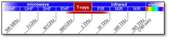
Metamaterials are materials which are made of artificially tailored structures by changing the internal homogeneous electromagnetic structures and composed of metals and dielectrics. Hence, these metamaterials consist of exotic properties such as negative refraction coefficient, cloaking, negative mass inertia, perfect absorption, and negative modulus of elasticity. Based on these unique properties, metamaterials are commonly used in wide variety of engineering applications. These metamaterials can be uniquely designed to achieve special materials which do not exist in nature and hence more research have been undergoing to analyze these materials. They are commonly used in satellite trackers as well as in computer chip that gives access to fast processing of data. It can also be used in imaging solutions that uses microwaves to form images without the need for a lens or any kind of movement control. They are also used in antennas to filter the frequency and accept the required signals as well as in energy harvesting, invisibility cloaks etc. There are many types of metamaterials that have been tested and used for different applications by many researchers and the amount of work done have increased exponentially over the last few years. These metamaterials have branched out too many ideas and possibilities that have greater impact on everyday life situations [1, 2]. Metamaterials are fabricated either by electron beam lithography vapor deposition or absorbed ion beam patterning [3]. Figure 1 shows the electromagnetic waves or electromagnetic spectrum with respect to frequency regimes which extends below the low frequencies used for modern radio waves to gamma rays at the short wavelength [4]. Based on the Figure 1 it is observed that there are many ways to study metamaterials in different frequency ranges.
Solar energy is one of the most prominent to have greater potential for tapping power, as it has multiple ways to use it either by absorbing the heat or the sun light emission as compared to other conventional energy harvesting techniques. Solar cell is the best option to gather energy by directly converting the sunlight into electricity. Using metamaterials, it is possible to improve solar cell by modifying their structural patterns or improve their technical limitations. In this research paper, the characteristics of metamaterials is developed for perfect absorbers in microwave frequency regime, Terahertz regime, frequency selective surfaces and negative refractive index materials. Based on these some of the literature have been included in this research article to know the merits of using metamaterials in solar energy applications. Hossain et al. [5] have studied a solar cell based on metamaterial absorber (PMA) and verified its significance in terms of increase in efficiency of absorption which works in visible frequency range. They concluded that using this metamaterial, it is possible to develop renewable solar energy cell which works in visible frequency range. Shin et al. [6] have studied photothermal and thermoplasmonic metamaterials used as photovoltaic devices in case of solar energy applications. They concluded that these hybrid systems have more power conversion efficiency as the amount of heat loss is less as compared to individual metamaterials. Bagmanci et al. [7] has designed and numerically demonstrated ultra-broadband metamaterial absorber used for solar energy applications. The operational frequencies of these metamaterials are lying between 430-770 THz. They concluded that the designed metamaterials structure can be used in solar energy applications in the visible light range frequency. Wang and Cheng [8] have studied nanoparticles and metamaterials in the range of visible and near infrared wavelengths with applications to renewable solar energy. Finite difference time domain (FDTD) and rigorous coupled wave analysis (RCWA) are the two methods adapted to study absorption properties of nanomaterials and metamaterials. They concluded that these study helps in understanding the physical mechanism in absorption of solar energy in case of above materials. Herold et al. [9] have studied and proposed compact tunable metamaterials absorber for solar applications which can be used in visible frequency range. They concluded that these proposed materials can be used in solar cell applications. Tan et al. [10] have studied energy harvesting and absorbing using metamaterials. They studied different literatures considering acoustic, mechanical, electro-magnetic, thermal energy harvesting using metamaterials. They concluded that this metamaterial is having a great impact in smart cities and sustainable developments. Pan et al. [11] has studied hyperbolic metamaterials which operates in the frequency range of visible and infrared light. They have observed the high absorption peaks between 0.4 µm and 0.3 µm for normal incidence on a plane wave. They concluded that absorbers with larger periodic unit cell has better absorption in case of visible and infrared waveband and can be used for different applications. Fedotov [12] has studied metamaterial artificial material composites that have more physical properties as compared to the materials which is available in nature. They are commonly used in antennas and waveguide engineering, imaging, microscopy, sensing and light manipulations applications. They concluded by giving basic principle, design rules and various tricks to achieve these desired properties.
Figure 1. Electromagnetic spectrum with respect to frequency regimes
It is very well known that the equations for describing the propagation of electromagnetic waves through media and their interaction with matter are the Maxwell’s equations, and they are the main topics of many textbooks, such as Jackson [13], Brau [14], Reitz [15], and so on.
Metamaterials have been designed fabricated and experimented in every spectral range, from radio, microwave, infrared and optical range. Metamaterials interacting with waves are electromagnetic waves with frequencies lower than infrared are called metamaterials operating in Gigahertz (GHz) regime. Similarly, metamaterials interacting with waves are electromagnetic waves with frequencies higher than microwaves are called metamaterials operating in Terahertz (THz) regime. Metamaterials in the terahertz regime mainly used for controlling the radiation due to their electric and magnetic properties. Metamaterials operating in GHz and THz regime have wide applications as absorbers, modulators, filter, waveguide, resonator and antenna and molecular sensors. From the above literature review it is observed that many researchers have worked on metamaterials considering visible frequency region and infrared light region operating in Gigahertz region and Terahertz region. So, in this research papers authors have considered metamaterial consisting of three different structures and tried to study.
Metamaterial absorbers are of two types 1-broadband absorbers and 2-resonant absorbers, so far as confirmed the latter group can have perfect absorption in a narrow bandwidth, it is possible to make it operate in broadband range by stacking several layers, but this will create a disadvantage of heavy weight and bulkiness. Metamaterial based perfect absorbers are somehow kind of resonant absorbers, more specifically circuit-analogs (CA), The metamaterial based on perfect absorber structure consists of following 1- a layer of periodically arranged metallic patterns 2- a dielectric layer 3- a continuous metallic layer. To accomplish total absorption there should be no reflection or transmission, which will be a feat carried by the three layers as discussed above.
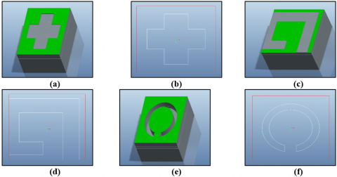
Some examples of the structures commonly studied in the metamaterial research are shown in Figure 2.
Figure 2. Examples of metamaterial structures
No transmission can be carried out by the third layer, blocking completely all incident Electromagnetic waves, The second layer which is the dielectric layer provides space to the incident EM wave to stay and be absorbed, It is generally believed that to make sufficient space for the incident wave, it is desirable to use high real part electric permittivity material because it reduces the thickness of dielectric layer with the optical path still maintained. For the incident wave, the path should be given by ND, where n is the refractive index and d is the distance travelled. Dielectric layers have very small imaginary part of permittivity, but it is important for the absorption of incident wave and depends on the specific design. Sometimes it plays an important role as for instance, the Fabry Perot cavity [16], and in case of Salisbury screen [17]. It is observed that dielectric layer does not only provide space for the cavity resonance but, also it produces another absorption resulting in dual band absorption.
The first layer is regalia of patterned metallic unit. The patterning is done for the following two reasons, first reason is the transmittance at the first layer is led by a certain sonorousness at the targeted frequency regimen, secondly the first layer free acts not only as passive, but an active role and there should be no reflection on it. This no reflection is achieved by matching the impedance of the first layer to that of free space or vacancy. The incident wave does not have any way to card the difference since both the first layer and the other are optically identical. Ordinary bicycle materials do not possess the impedance matching with that environment. Only metamaterials whose geometric parametric quantity of metallic patterns are carefully adjusted can have those properties. These three layers build the required metamaterial absorber, but they work in different frequency ranges depending on the plasmon frequency and geometric parameters of the structure [18]. Some of the literature corresponding to Microwave spectrum in GHz and THz regime is shown in Table 1.
Table 1. Microwave spectrum observed in GHz regime
|
GHz range/ Microwave spectrum |
||||
|
Type |
Absorption or reflection rate |
Structure |
Remarks |
Reference |
|
First perfect absorption |
Absorption apex of 88 % at 11.5 GHz. |
ERR on the front side and cut wire on the rear one, separated by a dielectric substrate. |
Able to decouple ɛ and μ and individually tune the resonance. |
Landy et al. [19] |
|
Dual-band metamaterial absorber |
Absorption points of 11.15 at 16.01 GHz |
ERR on the front layer and cut wire on the rear one, separated by a dielectric FR4 substrate |
Absorber may apprehend at other frequency range with nearly perfect absorption |
Li et al. [20] |
|
Double-negative (DNG) Metamaterial |
Negative refractive index from 3.482 to 14 GHz for the bandwidth of 3.61-2.406 GHz. |
Z-shape structure formed by splitting two arms of unit cell separated by FR-4 substrate material. |
Exhibits a negative refractive index (NRI) bandwidth of more than 3.6 GHz considering the frequency from 2 to 14 GHz. |
Hasan et al. [21] |
|
THz range/ Infrared spectrum |
||||
|
Perfect absorption Metamaterial |
Absorption of 0.70 at 1.3 THz. |
Consists of ERR and a magnetic resonator; two discrete metallic elements. |
The EM can be tuned to engage the impedance to the free space and to minimize the reflectance at a specific frequency. |
Tao et al. [22] |
|
Terahertz metamaterial-broad and flat absorbers. |
At the incident angle of 60°, the peak absorptance is above 90%, and dip absorption dip is 74%. |
Double I-shaped resonators separated from a ground plane separated by a dielectric. |
Broad and flat due to the super position of individual components. |
Huang et al. [23] |
|
Broadband infrared metamaterial absorber. |
Absorbance of 97% over the mid-infrared regime from 4 to 7 μm. |
An arrangement of uniform aluminum disks separated by a Zinc Sulphide (ZnS) dielectric from the ground plane. |
It is transparent to visible light and flexible of using visible radiation to control the metamaterial. |
Dayal et al. [24] |
The material selection and the layout of the structure considered for metamaterial-based absorber in this study is described as follows. Different configurations have been studied considering various structure of the material. The numerical model has been created using 3 different structures and the experimental protocol is simulated to perform data analysis initially and the graphs of the disturbances have been captured for these structures to check transmission and reflectivity.
Structure 1
The structure 1 is composed of single band THz metamaterial absorber. This structure is basically an electric ring (LC shaped structure) resonator (ERR) and is cross made of metal separated by a dielectric layer on top of a metal ground plane as shown in Figure 3(a) and Figure 3(b). This structure responds significantly to uniform electric fields but responds marginally to a magnetic field. The magnetic component of the incident THz wave induces the current in the ERR by coupling the (ERR) with a ground plane. The first structure consists of 2 $\mu m$ cross shaped ERR followed by a 3 $\mu m$ m polyimide dielectric substrate and third final layer which is 2 $\mu m$ metallic ground plane. The THz polyimide material properties is having a refractive index of 1.68 and the value of electrical conductivity is 0.06. while the resonator and metallic ground plane are treated as perfect electric conductor.
Structure 2
This structure composes of also tunable bandwidth THz metamaterial absorber, the device consists of an inverted C-shaped without the curve and metal ground plane separated by a dielectric layer which share different type of materials. This structure according to the simulation, it can have fluctuated resonance frequency which can produce two absorption peaks if the metamaterial substrate (dielectric) thickness is changed and is as shown in Figure 3(c) and 3(d). This consists of uniquely shaped structure that cannot be described significantly, the polyimide is 8 $\mu m$ thickness followed by 200 nm uniquely shaped first layer and metallic ground plane, the electric conductivity of the resonator is 4.09×10⁷ V/m.
Structure 3
This structure is composed of frequency selective surface that uses Floquet periodic condition (Branch of theory of ordinary differential equations) to solve the frequency domain of complementary split ring resonator, to show the parametric sweep in resonance frequency to clarify transmission and reflectivity of the material. This structure consists of Complementary Split Ring Resonator structure (CSRR) with a radius of 5 metamaterial, width of 1.5 metamaterial and gap size of 1.5 metamaterial. The material has relative permittivity of 2.1, relative permeability is unity and no electrical conductivity and is as shown in Figure 3(e) and Figure 3(f). The corresponding frequencies for the above selected materials are as shown in Table 2. The numerical approaches used for simulations are the 1. Plane wave expansion 2. Finite difference time domain method 3. Transfer matrix method 4. Finite element method.
Table 2. Frequency and bandwidth for various shaped structures
|
First Layer |
Dielectric Layer |
Metallic Plane |
Frequency Range |
Bandwidth |
|
LC shaped structure (gold) |
Polyimide |
Gold |
0.8 THz-2.4 THz |
Tunable Band |
|
Cross shaped ERR (silver) |
Polyimide |
Silver |
1 THz-4 THz |
Single Band |
|
Split ring resonator |
Air |
Air |
3.8 GHz-5.4 GHz |
Single Band |
The simulation has been carried out using two different tools i.e. COMSOL Multiphysics and Numerical FDTD Solutions.
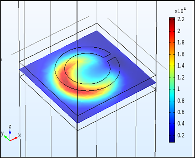
For structure 1 shown in Figure 3(a) and Figure 3(b) the electric ring resonator, FDTD solutions is used, the polyimide material is added with its complex refractive index, n = 1.68 - 0.06j and treating the ERR and the metallic plane as PEC (Perfect Electric Conductor), the source is defined as plane wave and setting the minimum and maximum frequency from 1 THz to 4 THz. Figure 4 shows the electric field distribution analysis for the structure 1 and the corresponding absorption rate versus frequency is as shown in Figure 5.
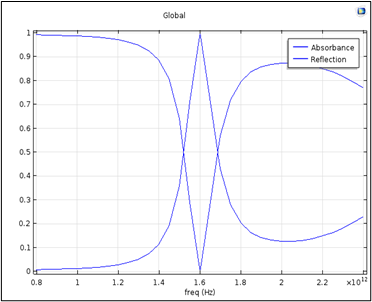
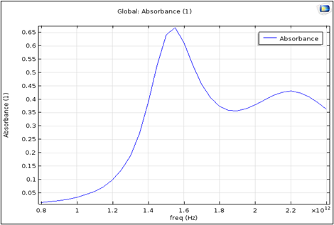
For the structure 2 shown in Figure 3 (c) and Figure 3(d), the analysis was carried out using COMSOL Multiphysics. The resonator is made of Gold as like that of ground plane, where the dielectric layer is the polyimide with a complex refractive index. The gap is filled with an increased electric field as the frequency passes by, the resonator provides an absolute absorption at frequency range of 1.6 THz, and changes if the substrate thickness is adjusted. The corresponding graph of absorption and reflection versus frequency of metamaterial absorber is as shown in Figure 6 and Figure 7. When the substrate thickness changed to 14 $\mu m$, a flawed dual band absorption is obtained, as shown in Figure 8 the first peak of absorbance is lesser than it was with 8 $\mu m$ thickness substrate.
Finally, the structure 3 shown in Figure 3(e) and Figure 3(f) which is the complementary split ring resonator structure (CSRR), it acts as a frequency selective surface, or as well-known as a bandpass filter. Here we test various incident angles to check the reflectivity and transmissivity across a decent polarization state and the corresponding electric field distribution is as shown in Figure 9. Strong fields are observed inside the slot as shown in the slice Figure 9 where the electric field norm shows on the CSRR. The S parameter, which is the reflection coefficient that has been obtained through transmission line theory is as shown in Figure 10. From this figure it is observed that the S parameters from the electromagnetic waves port has a resonance frequency at 4.6 GHz.
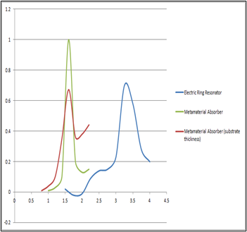
Figure 11 shows the comparison of absorptivity of all THz metamaterial absorbers. From this it can be concluded that metamaterial absorber CSRR has high absorptivity as compared to ERR and metamaterial absorber (Substrate thickness).
Dimensions and specifications of the structures:
Figure 3. a) Schematic 3D diagram of the cross shaped structure, b) 2D shape of the cross shaped structure c) 3D diagram of uniquely shaped structure, d) 2D uniquely shaped structure e) 3D CSRR, Frequency selective surface, f) 2D CSRR, frequency selective surface
Figure 4. Electric field distribution analysis for cross shaped metamaterial absorber
Figure 5. Metamaterial absorber graph of absorption rate vs frequency (ERR)
Figure 6. Electric field distribution analysis for uniquely shaped metamaterial absorber
Figure 7. Metamaterial absorber graph of absorption and reflection vs Frequency of metamaterial absorber
Figure 8. Metamaterial absorber graph of absorbance vs frequency (substrate thickness 14um)
Figure 9. Electric field distribution for CSRR
Figure 10. Reflectivity and transmissivity vs frequency graph of CSRR
Figure 11. Comparison of absorptivity of all THz metamaterial absorbers
Three different metamaterial absorber structures and their responses have been studied. The metallic absorber structures enable very high absorption over the energy-rich portion of the solar spectrum and low thermal radiation at GHz and THz Regime. It can be concluded that all structures reached a maximum point of absorption but, in a narrow bandwidth due to implications on the substrate material. Broadband materials can be obtained if more than one layer is stacked to represent the transverse magnetic waves. Apart from this limitation, it can be used as a frequency detector for THz applications, but to use it, it should be polarization and incident angle insensitive.
Metamaterials can be used in wide varieties of application but based on the findings the material can play a vital role for energy solutions especially in the field of sustainable energy. Electromagnetic waves can be harvested using metamaterial to produce electricity. This works like a solar panel where it absorbs not just the visible spectrum of lights but also infrared and ultraviolet radiation thus increasing the total efficiency of a solar panel. It is also possible to market this material to retrofit existing solar panels to keep cost down and increase efficiency while keeping the footprint of the solar panel unchanged.
[1] Li, L.Y., Wang, J., Du, H.L., Wang, J.F., Qu, S.B., Xu, Z. (2015). A band enhanced metamaterial absorber based on E-shaped all-dielectric resonators. AIP Advances, 5(1): 017141-017149. https://doi.org/10.1063/1.4907050
[2] Salisbury, W.W. (1952). Absorbent Body for Electromagnetic Waves. US Patent 2599944 (1952).
[3] Wendt, J.R., Burckel, D.B., Eyck, G.A.T., Ellis, A.R., Brener, I., Sinclair, M.B. (2010). Fabrication techniques for three-dimensional metamaterials in the midinfrared. Journal of Vacuum Science and Technology, 28(6): C6030-C6033. http://dx.doi.org/10.1116/1.3504586
[4] Padilla, W. (2014). Exploring Technology’s “Tetrahertz Gap”, Center for Metamaterials and Integrated Plasmonics, Technical Report.
[5] Hossain, M.J., Faruque, M.R.I., Islam, M.T. (2018). Perfect metamaterial absorber with high fractional bandwidth for solar energy harvesting. PLOS ONE, 14(1): 1-15. https://doi.org/10.1371/journal.pone.0211751
[6] Shin, D., Kang, G., Gupta, P., Behera, S., Lee, H., Urbas, A.M., Park, W., Kim, K. (2018). Thermoplasmonic and photothermal metamaterials for solar energy applications. Advanced Optical Materials, 6(18): 1-26. https://doi.org/10.1002/adom.201800317
[7] Bagmanci, M., Karaaslan, M., Unal, E., Akgol, O., Bakir, M., Sabah, C. (2019). Solar energy harvesting with ultra-broadband metamaterial absorber. International Journal of Modern Physics B, 33: 1-16. https://doi.org/10.1142/S0217979219500565
[8] Wang, Z., Cheng, P. (2019). Enhancements of absorption and photothermal conversion of solar energy enabled by surface plasmon resonances in nanoparticles and metamaterials. International Journal of Heat and Mass Transfer, 140: 453-482. https://doi.org/10.1016/j.ijheatmasstransfer.2019.05.085
[9] Herold, V.D.J., Dhavamani, J.M., Janapala, D.K. (2019). Step impedance resonator-based tunable perfect metamaterial absorber with polarization insensitivity for solar cell applications. International Journal of RF and Microwave Computer-Aided Engineering, 29(1): 1-7. https://doi.org/10.1002/mmce.21650
[10] Tan, T., Yan, Z., Zou, H., Ma, K., Liu, F., Zhao, L., Peng, Z., Zhang, W. (2019). Renewable energy harvesting and absorbing via multi-scale metamaterial system for internet of things. Applied Energy, 254: 113717. https://doi.org/10.1016/j.apenergy.2019.113717
[11] Pan, Q.H., Hong, J.R., Xu, S.D., Shuai, Y., Tan, H.P. (2018). Theoretical analysis of a hyberbolic metamaterial for harvesting visible and infrared light. Heat Transfer Engineering, 40(5-6): 410-417. https://doi.org/10.1080/01457632.2018.1432020
[12] Fedotov, V. (2017). Metamaterials. Springer Handbook of Electronic and Photonic Materials, Springer handbook series. Springer, Cham. https://doi.org/10.1007/978-3-319-48933-9_56
[13] Jackson, J. (1998). Classical Electrodynamics. Wiley; 3rd Edition.
[14] Brau, C. (2004). Modern Problems in Classical Electrodynamics. Oxford University Press.
[15] Reitz, J., Milford, F., Christy, R. (2009). Foundations of Electromagnetic Theory. San Francisco, Calif.: Pearson/Addison-Wesley, 2009.
[16] Rhee, J.Y., Yoo, Y.J., Kim, K.W., Kim, Y.J., Lee, Y.P. (2014). Metamaterial-based perfect absorbers. Journal of Electromagnetic Waves and Applications, 28(3): 1541-1580. https://doi.org/10.1080/09205071.2014.944273
[17] Zheng, H.Y., Jin, X.R., Park, J.W., Lu, Y.H., Rhee, J.Y., Jang, W.H., Cheong, H., Lee, Y.P. (2012). Tunable dual-band perfect absorbers based on extraordinary optical transmission and Fabry-Perot cavity resonance. Optics Express, 20(21): 24002-24009. https://doi.org/10.1364/OE.20.024002
[18] Hu, H.L., Peng, J.W., Lee, C.Y. (2018). Dynamic simulation of a Metamaterial beam consisting of tunable shape memory material absorbers. Vibration, 1(1): 81-92. https://doi.org/10.3390/vibration1010007
[19] Landy, N.I., Sajuyigbe, S., Mock, J.J., Smith, D.R., Padilla, W.J. (2008). Perfect metamaterial absorber. Physical Review Letters, 100(20): 207401-4. https://doi.org/10.1103/PhysRevLett.100.207402
[20] Li, M., Yang, H.L., Hou, X.U., Tian, Y., Hou, D.Y. (2010). Perfect metamaterial absorber with dual bands. Progress in Electromagnetics Research, 108: 37-49. https://doi.org/10.2528/PIER10071409
[21] Hasan, M., Faruque, M.R.I., Islam, S.S., Islam, M.T. (2016). A new compact double-negative miniaturized metamaterial for wideband operation. Materials (Basel), 9(10): 830. https://doi.org/10.3390/ma9100830
[22] Tao, H., Landy, N.I., Bingham, C.M., Zhang, X., Averitt, R.D., Padilla, W.J. (2008). A metamaterial absorber for the tetrahertz regime: Design, fabrication and characterization. Optics Express, 16(10): 7181-7188. https://doi.org/10.1364/OE.16.007181
[23] Huang, L., Chowdhury, D.R., Ramani, S., Reiten, M.T., Luo, S.N., Taylor, A.J., Chen, H.T. (2012). Experimental demonstration of tetrahertz metamaterial absorbers with a broad and flat high absorption band. Optics Letters, 37(2): 154-156. https://doi.org/10.1364/OL.37.000154
[24] Dayal, G., Ramakrishna, S.A. (2014). Broadband infrared metamaterial absorber with visible transparency using ITO as ground plane. Optics Express, 22(12): 15104-15110. https://doi.org/10.1364/OE.22.015104